

Page 1
Dual Conversion AM Receiver TDA 4360X
1 Overview
1.1 Features
• High flexibility with an external preamplifier stage
• Sym. or asym. mixer input
• 2-pin oscillator for the 1. LO
• 1. LO with LC tank circuit
• 1. LO at 100 MHz range
• Low narrow band noise
• Divider for 1. LO by 10 for the 100 kHz … 2 MHz range
and by 8 for the 2 MHz … 6 MHz range
• Integrated AGC generation
• Strictly symmetrical RF path
• Decoupled counter output
• 2. LO with quartz or external source
• Output for gain controlled 2. IF
• Switchable AGC time constant
P-DSO-28-1
Type Ordering Code Package
TDA 4360X Q67000-A5181 P-DSO-28-1
1.2 Application
The TDA 4360X is an integrated dual conversion AM receiver for use in car radios.
The input signal passes a linear mixer for conversion into the 1. IF (~ 10 MHz). Via an
external bandpass filter (CER filter, quartz filter) the 1. IF is converted in a second linear
mixer to the 2. IF (~ 460 kHz).
After an external narrowband selectivity (CER filter) the 2. IF passes an automatic gain
controlled (AGC) amplifier and is then demodulated to the AF. The AGC time constant
can be switched with a ratio of 20.
For counter controlled search tuning stop (STS) the frequencies of the 1. LO and the
2. IF are available.
Semiconductor Group 1 04.96
Page 2
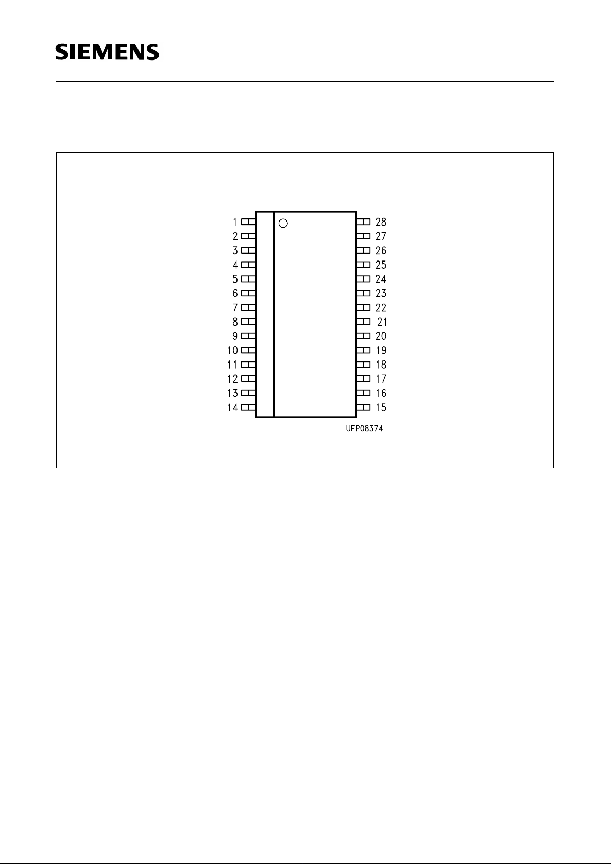
1.3 Pin Configuration
(top view)
TDA 4360X
P-DSO-28-1
Figure 1
Semiconductor Group 2 04.96
Page 3
1.4 Pin Definitions and Functions
Pin No. Function
TDA 4360X
1, 2
3
4
5
6
7, 8
9
10
11
12
13
Sym. Input for the AM signal in the frequency range of 100 kHz (SW) to 6.2
MHz (49m-Band) sym. application is recommended, asym. application is
possible
DC voltage alters the threshold voltage of the prestage AGC circuit.
GROUND: All DC values are referred to this pin
Buffered output for the by n divided (n = 8 or 10) oscillator frequency
Output for the internal reference voltage. This pin is to be blocked with a
ceramic capacitor to ground.
The ext. LC circuit between pin 7 and pin 8 determines the oscillator
frequency.
Supply voltage. This point is to be blocked to ground for AF and for RF
signals.
Buffered output for the oscillator frequency
Input for the frequency divider. Low voltage to pin 11 divides the oscillator
frequency by 8, high voltage or open input divides by10.
Blocking capacitor for the IF AGC circuit to suppress AF frequencies
Input to select the fast or slow AGC time constant
14
15
16
17, 18, 19
20
21, 22
23, 24
25
26
27, 28
Buffered AF output
Buffered output for the limited lower IF frequency. This signal is necessary
for an IF Counter Tuning System.
Buffered output for the AGC controlled lower IF signal. This pin is connected
to the AM stereo decoder.
Input pins for the DC coupled AGC amplifier
Open collector output of mixer for the lower IF (~ 450 MHz). A DC
connection to the tank circuit to
V
is recommended.
ref
Sym. mixer 2 input for the upper IF (~ 10.7 MHz). Asym. operation is
possible. The input signal is converted to the lower IF corresponding the
equation
f
LIF
= f
UIF
– f
2.LO
.
Input for the 2. local oscillator (LO). The pins can be connected via a quartz
or the oscillator is to be forced with an ext. signal.
Blocking capacitor for the prestage AGC
A capacitor to ground determines the AGC time constant. The DC potential
at this pin can be used for controlling the FET in the ext. prestage.
Sym. collector output of the mixer 1. The external tank circuit is tuned to the
upper IF.
Semiconductor Group 3 04.96
Page 4
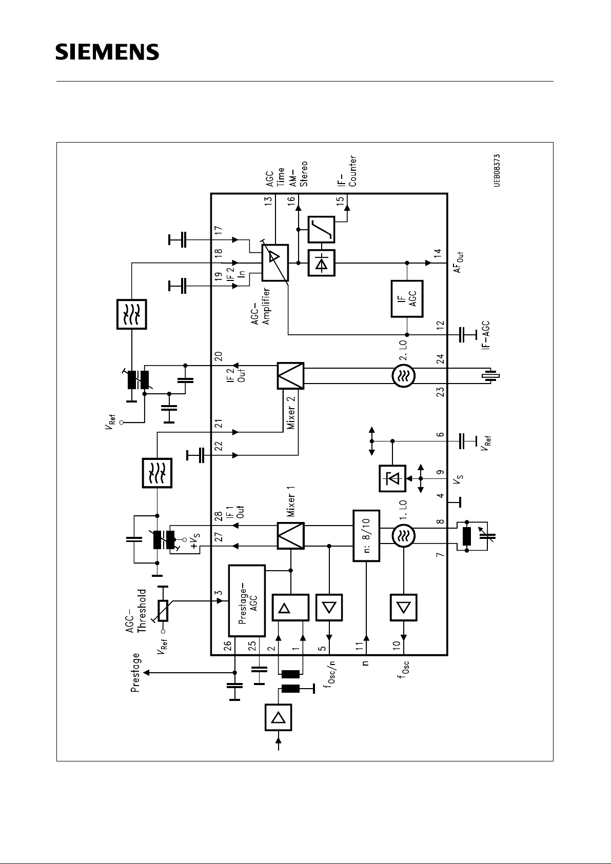
1.5 Functional Block Diagram
TDA 4360X
Figure 2
Block Diagram
Semiconductor Group 4 04.96
Page 5

TDA 4360X
2 Circuit Description
The integrated circuit includes an 2-pin oscillator (1. LO) with sym. input, buffered output
and a double balanced mixer with sym. input. These stages convert the AM input signal
to a 1. IF which is much higher (~ 10 MHz) than the input frequencies. The 1. LO
operates as a LC varactor oscillator in the same 100 MHz range like the FM tuner
oscillator (e.g. TUA 4310X). So the same peripheral elements can be used.
Depending on the signal strength the prestage AGC controls MOSFET prestage
amplifiers.
The 1. IF passes an external selectivity and is then converted in a sym. double balanced
mixer to the 2. IF.
The 2. LO operates as a quartz controlled oscillator or as an amplifier for an external
signal.
The 2. IF signal passes an automatic gain controlled (AGC) IF amplifier and is then
demodulated to the AF in a quasi-synchronous demodulator. The AGC time constant
can be switched with a ratio of 20.
For fine tuning the decoupled 2. IF frequency is available.
The TDA 4360X is prepared to work with a PLL in the 100 MHz range. When applied
with a standard AM-PLL the oscillator frequency divided by 8 or 10 has to be used. In
this case a higher phase noise is to be expected.
Semiconductor Group 5 04.96
Page 6

TDA 4360X
3 Electrical Characteristics
3.1 Absolute Maximum Ratings
T
= – 40 °C to 85 °C
A
Parameter Symbol Limit Values Unit Remarks
min. max.
ESD
Supply voltage
Mixer 1 output
Mixer 2 output
Mixer 2 input
AGC threshold
Mixer 1 input
f
OSC/n
f
OSC
Divide by n
V
Ref
I
Ref
2. LO
AGC amplifier input
IF counter
V
ESD
V
S
V
27
V
20
V
21, 22
V
3
V
1, 2
V
5
V
10
V
11
V
6
I
6, 0
V
23, 24
V
17 … 19
V
15
, V
28
– 4 + 4 kV HBM
0 13.2 V
0 13.2 V
0 13.2 V
0 13.2 V V 1.5 kΩ, 100 pF
05 V
05 V
013 V
013 V
05 V
05 V
03 mA
05 V
05 V
0 13.2 V
AM stereo output
AF output
IF AGC
V
V
V
16
14
12
0 13.2 V
0 13.2 V
0 13.2 V
Note: Maximum ratings are absolute ratings; exceeding only one of these values may
cause irreversible damage to the integrated circuit.
Semiconductor Group 6 04.96
Page 7

TDA 4360X
3.2 Operating Range
Parameter Symbol Limit Values Unit
min. max.
Supply voltage
Ambient temperature
V
T
S
A
7.5 13.2 V
– 40 + 85 °C
Note: In the operating range the functions given in the circuit description are fulfilled.
3.3 AC/DC Characteristics
V
= 10 V, TA = + 25 °C, f
S
= 10.7 MHz, f
IF1
= 456 kHz, fi = 1MHz
IF2
Parameter Symbol Limit Values Unit Test Condition Test
Circuit
Current
min. typ. max.
I
S
55 mA
consumption
Mixer 1
V
Intercept point
110 dBµV
≥ 100 mVrms
i
3. order
Mixer gain 5 dB
Max. input
V
i
600 mVpp
voltage
Noise figure
F
10 dB
(10 MHz)
1. LO
Frequency
f
1.LO
100 140 MHz
range
Counter output
V
C
100 mVpp
V
= 10 mV,
in
1.8 kΩ load
Semiconductor Group 7 04.96
Page 8

TDA 4360X
3.3 AC/DC Characteristics (cont’d)
V
= 10 V, TA = + 25 °C, f
S
Parameter Symbol Limit Values Unit Test Condition Test
= 10.7 MHz, f
IF1
min. typ. max.
= 456 kHz, fi = 1MHz
IF2
Circuit
Divided
100 mVpp
counter output
Divide by 8 0.7 V
Divide by 10 2.4 V
Output
R
C
330 Ω
impedance
Mixer 2
Mixer gain 3 dB
Noise figure F 10 dB
2. LO
Frequency range
External force
f
2.LO
15 MHz
30 mVrms
voltage
V
= 10 mV,
in
1.5 kΩ load
Prestage AGC Output
AGC voltage
AGC voltage
V
V
AGC1
AGC1
5.8 7.2 V VDC = 2 V;
V
= 100 mVrms
i
0 0.5 V VDC = 4 V;
V
= 100 mVrms
i
AGC Amplifier
AGC range 66 dB 1
AGC voltage
Reg. output
V
V
AGC2
IF
2.0 4.8 V V18 = 0/100 mVrms 1
30 mVrms 1
voltage
Input sensitivity
Semiconductor Group 8 04.96
V
– 3dB
50 µVrms 1
Page 9

TDA 4360X
3.3 AC/DC Characteristics (cont’d)
V
= 10 V, TA = + 25 °C, f
S
Parameter Symbol Limit Values Unit Test Condition Test
= 10.7 MHz, f
IF1
min. typ. max.
= 456 kHz, fi = 1MHz
IF2
Circuit
AGC current I
AGC current
I
AGC
AGC
– 500 µA V18 = 10 mVrms,
– 25 µA V18 = 10 mVrms,
Demodulator
AF output voltage
AF output voltage
Total harm.
V
Audio
V
Audio
k1%
180 mVrms Vi = 10 mV, m = 0.3 1
480 mVrms Vi = 10 mV, m = 0.8 1
distortion
Input voltage for
V
i
10 µVrms m = 0.3 1
S + N/N = 6 dB
Input voltage for
V
i
60 µVrms m = 0.3 1
S + N/N = 26 dB
S + N/N 60 dB
AF linearity ∆
V
Audio
3 dB 100 µV/100 mV 1
V
≥ 2.4 V
13
V
≤ 0.7 V
13
V
= 10 mV, m = 0.8 1
i
V
= 10 mV, m = 0.8 1
i
1
1
IF Counter
IF counter output
V
C
100 mVrms 1
voltage
Note: The listed characteristics are ensured over the operating range of the integrated
circuit. Typical characteristics specify mean values expected over the production
spread. If not otherwise specified, typical characteristics apply at
T
= 25°C and
A
the given supply voltage.
Semiconductor Group 9 04.96
Page 10

TDA 4360X
Figure 3
Test Circuit
Semiconductor Group 10 04.96
Page 11

TDA 4360X
Figure 4
Application Circuit
Semiconductor Group 11 04.96
Page 12

4 Package Outlines
P-DSO-28-1
(Plastic Dual Small Outline Package)
TDA 4360X
Sorts of Packing
Package outlines for tubes, trays etc. are contained in our
Data Book “Package Information”.
SMD = Surface Mounted Device
GPS05123
Dimensions in mm
Semiconductor Group 12 04.96
 Loading...