

Page 1
FM-IF with Counter Output, Field Strength Indicator,
Noise Detector and MUTE Setting
1 Overview
1.1 Features
• 7-stage limiter amplifier
• Coincidence demodulator
• Counter output with request input
• Field strength output
• Multipath identification circuit
• Adjustable muting depth (with full muting ≥ 80 dB)
• This device is ESD protected
P-DSO-16-1
TDA 4320X
Type Ordering Code Package
TDA 4320X Q67000-A-5000 P-DSO-16-1
Semiconductor Group 35 04.96
Page 2
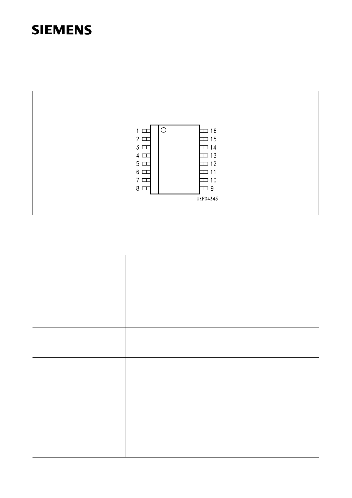
1.2 Pin Configuration
(top view)
TDA 4320X
P-DSO-16-1
Figure 1
1.3 Pin Definitions and Functions
Pin No. Symbol Function
1 GND Ground
Decoupling capacitors for bias, VS and V
connected directly to Pin 1
2 Multipath
identification input
Multipath identification input
High impedance input (
the filtered field strength output (high pass or band pass).
3 Rectifier time
constant
Rectifier time constant
Determines the attack and release time of the
identification circuit.
4 Multipath
identification
output
Multipath identification output
Open npn-collector output, which is low during
(V4/V1 ≤ 0.7 V) multipath interference.
Pins are to be
REF
R
~10kΩ). This input receives
i
5 MUTE input MUTE input
For DC voltage (usually derived from field strength output
voltage) which attenuates the AF output voltage by the
setting muting depth (Pin 7). Max. attenuation when
V
= 0 V, no attenuation when V5≥ 0.5 V.
5
6 AF output AF output
Demodulated FM-IF.
Semiconductor Group 36 04.96
Page 3
1.3 Pin Definitions and Functions (cont’d)
Pin No. Symbol Function
7 MUTE depth MUTE depth
Adjustment by connecting a dc voltage to ground the
requested muting depth can be set. Maximal attenuation
of AF output voltage with
attenuation with
V
≤ 1V (≥80 dB).
7
V
7
TDA 4320X
V
= 2.4 V (typ. 38 dB), minimal
7
= 4.8 V (typ. 0 dB). Full muting with
8 Demodulator
tank circuit
Demodulator tank circuit
Driven via two on-chip capacitors (approx.15 pF ± 25 %).
The tank circuit voltage should be typ. 400 mVpp.
9 Demodulator
Demodulator circuit
circuit
10 Reference
voltage
Reference voltage
Should be RF decoupled to Pin 1.
11 IF counter output IF counter output
Provides the IF carrier frequency (low impedance output
R
≈ 1.5 kΩ).
out
12
V
S
Supply voltage
RF decoupled to Pin 1
13 Field strength
output
Field strength output
Supplies a DC voltage proportional to the IF input level
with very low delay time.
14 Field strength
adjust
Field strength adjust
Adjustment of slope and starting point of field strength
output voltage
15 IF input bias IF input bias
To be RF decoupled to Pin 1
16 IF input IF input
FM-lF input
Semiconductor Group 37 04.96
Page 4
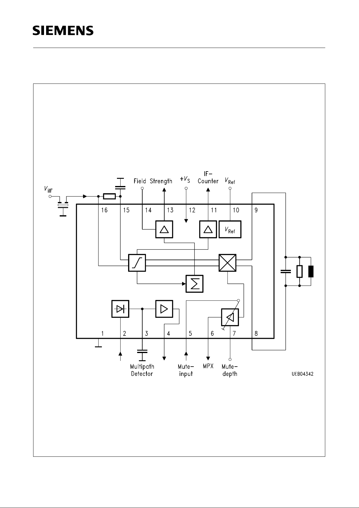
1.4 Functional Block Diagram
TDA 4320X
Figure 2
Semiconductor Group 38 04.96
Page 5

TDA 4320X
2 Functional Description
The FM-IF demodulator TDA 4320X has been developed especially for car radio
applications. The on-chip multipath identification circuit activates an interference
suppression circuit in case of multipath interferences.
3 Circuit Description
The IC includes a 7-stage capacitive coupled limiter amplifier with coincidence
demodulator and AF output. The AF output signal can be continuously attenuated to
decrease the noise. In case of multipath interferences, the TDA 4320X includes an
identification circuitry. There is a field strength output (with min. 76 dB dynamic range,
typ. ± 1 dB nonlinearity and typ. ± 3 dB temperature drift), an IF counter output and an
adjustable muting (with full muting ≥ 80 dB).
Semiconductor Group 39 04.96
Page 6

TDA 4320X
4 Electrical Characteristics
4.1 Absolute Maximum Ratings
T
=–40°Cto+85°C
A
Parameter Symbol Limit Values Unit Remarks
min. max.
Supply voltage
Junction temperature
Storage temperature
Thermal resistance (system-air)
ESD voltage, HBM (1.5 kΩ, 100 pF)
V
T
T
R
V
S
j
S
thSA
ESD
0 13.2 V
150 °C
125 °C
105 K/W
–4 4 kV
Note: Maximum ratings are absolute ratings; exceeding only one of these values may
cause irreversible damage to the integrated circuit.
4.2 Operating Range
T
=–40°Cto+85°C
A
Parameter Symbol Limit Values Unit Remarks
min. max.
Supply voltage
Ambient temperature
V
T
S
A
7.5 13.2 V
–40 85 °C
Note: In the operating range the functions given in the circuit description are fulfilled.
Semiconductor Group 40 04.96
Page 7

TDA 4320X
4.3 AC/DC Characteristics
V
= 10 V; f
S
V
= 10 mV; TA = – 40 °C to + 85 °C
iIFrms
Parameter Symbol Limit Values Unit Test Condition Test
= 10.7 MHz; ∆f = 75 kHz; f
ilF
= 1 kHz;
mod
min. typ. max.
Circuit
Current consumption
Stabilized voltage
Field strength output
I
12
V
10
V
13
4.5 4.8 5.1 V V5= 4.8 V; V7=4V 1
30 mA V5= 4.8 V; V7=4V 1
V
= 4.8 V; V7=4V
5
– Dynamic range 80 dB D1
– Nonlinearity ± 1dB D2
– Temperature drift ± 3dB D3
– Load capacitance 50 pF
– Load resistance 1 kΩ
Input voltage for limiter
V
13
V
13
V
13
V
16
5.0 5.5 6.0 V V
2.2 2.7 3.2 V V
0 1.2 V V
30 µVrms V
= 200 mV 1
ilFrms
= 1 mV 1
ilFrms
= 0 mV 1
ilFrms
=–3dB 1
qAF
threshold
AF output voltage
Total harmonic distortion
AM suppression
V
qAF
THD
a
AM
qAF
480 840 mVrms V5= 4.8 V; V7=4V 1
1.2 % V5= 4.8 V; V7=4V 1
60 dB m =80% 1
Signal-to-noise ratio
Counter output voltage
Noise detector sensitivity
Charge current Pin 3
Discharge current Pin 3
76 dB
a
S/N
V
11
V
2
V
2
I
3
76 dB V5= 4.8 V; V7=4V 1
50 mVrms CL= 5 pF;
3.2 mVrms f2= 20 kHz 1
4.3 mVrms f2= 300 kHz 1
2.5 mA f2= 20 kHz;
2.5 mA
I
3
20 µA V
m =30% 1
1
R
= 1.5 kΩ
i11
1
V
≥ 6 mVrms
2
f
= 300 kHz;
2
V
≥7 mVrms
2
=0V 1
2AC
1
Semiconductor Group 41 04.96
Page 8

TDA 4320X
4.3 AC/DC Characteristics (cont’d)
V
= 10 V; f
S
V
= 10 mV; TA = – 40 °C to + 85 °C
iIFrms
Parameter Symbol Limit Values Unit Test Condition Test
= 10.7 MHz; ∆f = 75 kHz; f
ilF
= 1 kHz;
mod
min. typ. max.
Circuit
AF MUTE
Voltage for MUTE OFF
Voltage for MUTE ON
V
= 10 V; f
S
V
= 10 mV; TA = 25 °C
iIFrms
= 10.7 MHz; ∆f = 75 kHz; f
ilF
a
AF
–2 2 dB
30 38 46 dB
80 dB
80 dB
V
5
V
5
0.7 V 1
0V 1
0dBV
= 1 kHz;
mod
= 4.8 V; V7= 4.8 V D4
5
V
=0V;V7= 4.8 V D4
5
V
=0V;V7= 2.4 V D4
5
V
= 4.8 V; V7≤ 1.0 V D4
5
V
=0V;V7≤1.0 V D4
5
Parameter Symbol Limit Values Unit Test Condition Test
Circuit
Current consumption
Stabilized voltage
Field strength output
Dynamic range
min. typ. max.
I
12
V
10
V
13
4.6 4.8 5.0 V V5= 4.8 V; V7=4V1
30 mA V5= 4.8 V; V7=4V1
V
= 4.8 V; V7=4V
5
74 80 dB D1
Nonlinearity
Temperature drift
Load capacitance
Load resistance
Input voltage for limiter
1kΩ
V
13
V
13
V
13
V
16
5.1 5.5 5.9 V V
2.3 2.7 3.1 V V
0 1.1 V V
± 1dB D2
± 3dB D3
50 pF
= 200 mV 1
ilFrms
= 1 mV 1
ilFrms
= 0 mV 1
ilFrms
30 39 µVrms V
=–3dB 1
qAF
threshold
AF output voltage
Total harmonic distortion
AM suppression
V
qAF
THD
a
AM
qAF
550 650 750 mVrms V5= 4.8 V; V7=4V1
1.2 % V5= 4.8 V; V7=4V1
60 dB m = 80 % 1
76 82 dB m = 30 % 1
Semiconductor Group 42 04.96
Page 9

TDA 4320X
4.3 AC/DC Characteristics (cont’d)
V
= 10 V; f
S
V
= 10 mV; TA = 25 °C
iIFrms
Parameter Symbol Limit Values Unit Test Condition Test
= 10.7 MHz; ∆f = 75 kHz; f
ilF
= 1 kHz;
mod
min. typ. max.
Circuit
Signal-to-noise ratio
Counter output voltage
Noise detector sensitivity
Charge current Pin 3
Discharge current Pin 3
AF MUTE
a
S/N
V
11
V
2
V
2
I
3
I
3
a
AF
76 84 dB V5= 4.8 V;
V
=4V
7
50 80 mVrms CL= 5 pF;
R
= 1.5 kΩ
i11
2 3.2 6 mVrms f2= 20 kHz 1
2.7 4.3 7 mVrms f2= 300 kHz 1
1.6 2.5 4 mA f2= 20 kHz;
V
≥ 6 mVrms
2
1.6 2.5 4 mA
10 20 40 µA V
0dBV
–2 2 dB
32 38 44 dB
f
= 300 kHz;
2
V
≥ 7 mVrms
2
=0V 1
2AC
= 4.8 V;
5
V
= 4.8 V
7
V
=0V;
5
V
= 4.8 V
7
V
=0V;
5
V
= 2.4 V
7
1
1
1
1
D4
D4
D4
Voltage for MUTE OFF
Voltage for MUTE ON
80 dB
80 dB
V
5
V
5
0.5 V 1
0 0.1 V 1
V
= 4.8 V;
5
V
≤1.0 V
7
V
=0V;
5
V
≤1.0 V
7
D4
D4
Semiconductor Group 43 04.96
Page 10

Test Circuit 1
TDA 4320X
Figure 3
Semiconductor Group 44 04.96
Page 11

Application Circuit
TDA 4320X
Figure 4
Semiconductor Group 45 04.96
Page 12

Diagrams
Diagram D1
TDA 4320X
V
Dynamics
F
V
The dynamic range of
voltage is determined by the test points M1 through M4 as
F
follows:
M1: test point (at
M2: test point (at V
M3: test point (at V
M4: test point (at V
= – 60 dBm) supplies V
iIF
= – 20 dBm) supplies V
iIF
= – 90 dBm) supplies V
iIF
= + 5 dBm) supplies V
iIF
F
F
F
(M4)
F
(M1)
(M2)
(M3)
V
Hence follows:
M
M
V
Semiconductor Group 46 04.96
:= – 20 dBm + (V
VF max
:= – 60 dBµV – (V
VF min
F Dynamics
= M
VF max
– M
(M4) – VF(M2))/(VF(M2) – VF(M1)) × 40 dB
F
(M1) – VF(M3))/(VF(M2) – VF(M1)) × 40 dB
F
VF min
Page 13

Diagram D2
TDA 4320X
Test points to determine VF linearity:
V
is determined at 25 °C
F
Slope:
m = (V
The tolerance range of the
V
V
The
F max
F min
= V
= V
V
values within the VF dynamic range (M
F
(M2) – VF(M1))/40 dB.
F
V
-linearity is determined by two parallel lines:
F
(M1) + m(M + 60 dB + 1 dB)
F
(M1) + m(M + 60 dB – 1 dB)
F
predetermined tolerance range:
V
F min
≤ V
(M) ≤ V
F
VF min
F max
≤ M ≤ M
) must be inside the
VF max
Semiconductor Group 47 04.96
Page 14

Diagram D3
TDA 4320X
Test points to determine VF temperature drift:
V
-temperature drift: it is determined within – 40 to + 85 °C.
F
Slope:
m = (V
The tolerance range of the
V
V
The
(
F max
F min
M
= V
= V
V
values for temperatures between – 40 to + 85 °C within the VF dynamic range
F
≤ VF ≤ M
VF min
(M2) – VF(M1))/40 dB (at 25 °C).
F
V
-temperature is determined by two parallel lines:
F
(M1) + m(M + 60 dB + 3 dB)
F
(M1) + m(M + 60 dB – 3 dB)
F
) must be inside the predetermined tolerance field:
VF max
V
F min
≤ V
(M) ≤ V
F
F max
Semiconductor Group 48 04.96
Page 15

Diagram D4
Mute Characteristics
TDA 4320X
Semiconductor Group 49 04.96
Page 16

5 Package Outlines
P-DSO-16-1
(Plastic Dual Small Outline Package)
TDA 4320X
Sorts of Packing
Package outlines for tubes, trays etc. are contained in our
Data Book “Package Information”.
SMD = Surface Mounted Device
GPS05119
Dimensions in mm
Semiconductor Group 50 04.96
 Loading...