

Page 1
INTEGRATED CIRCUITS
DATA SH EET
TDA3827
TV-sound demodulator circuit with
SCART switches and AF control
Preliminary specification
File under Integrated Circuits, IC02
March 1991
Page 2
Philips Semiconductors Preliminary specification
TV-sound demodulator circuit with
SCART switches and AF control
FEATURES
• Wide supply voltage range from
4.5 V to 13.2 V
• Wide frequency range from 4 to
12 MHz
• High ripple rejection
• High precision and temperature
compensated FM-demodulator
output
• Multiple-input AF operational
amplifiers with offset compensation
• SCART AF input / AF output (low
impedance)
• External AF input
• High-level AF output voltage with
low distortion
• External selection of the source
selector AF gain
• Low switching noise between AF
and mute
• Wide volume-control range
QUICK REFERENCE DATA
SYMBOL PARAMETER CONDITIONS MIN. TYP. MAX. UNIT
V
P
I
P
(S+N)/N signal to weighted
V
5(rms)
V
13(rms)
G
v
V
17(rms)
THD total harmonic
supply voltage
range (pin 18)
supply current
(pin 18)
noise
FM demodulator
output voltage
(RMS value)
SCART output
signal
(RMS value)
volume control
range
AF output signal
(RMS value)
distortion (pin 17)
TDA3827
4.5 5.0 13.2 V
VP = 5 V − 26 − mA
V
= 12 V − 28 − mA
P
73 78 − dB
∆f = 50 kHz;
f
= 1 kHz;
mod
QL = 20
∆f = 50 kHz;
f
= 1 kHz;
mod
QL = 20
450 500 550 mV
− 1.0 − V
80 85 − dB
− 1.0 − V
− 0.5 − %
GENERAL DESCRIPTION
The TDA3827 contains a single FM
demodulator with SCART switches, a
mute function and volume control.
ORDERING AND PACKAGE INFORMATION
EXTENDED TYPE
NUMBER
PINS PIN POSITION MATERIAL CODE
PACKAGE
TDA3827 18 DIL plastic SOT102
Note
1. SOT102-2; 1996 December 13.
(1)
March 1991 2
Page 3
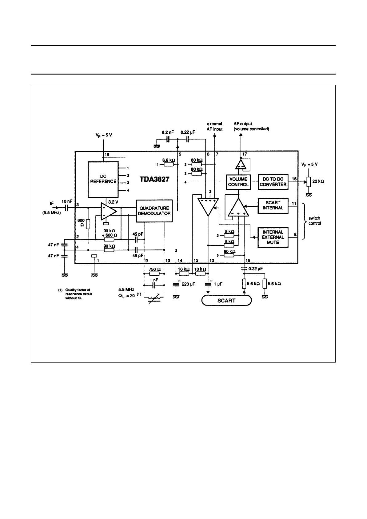
Philips Semiconductors Preliminary specification
TV-sound demodulator circuit with SCART
switches and AF control
TDA3827
Fig.1 Block diagram.
March 1991 3
Page 4
Philips Semiconductors Preliminary specification
TV-sound demodulator circuit with SCART
switches and AF control
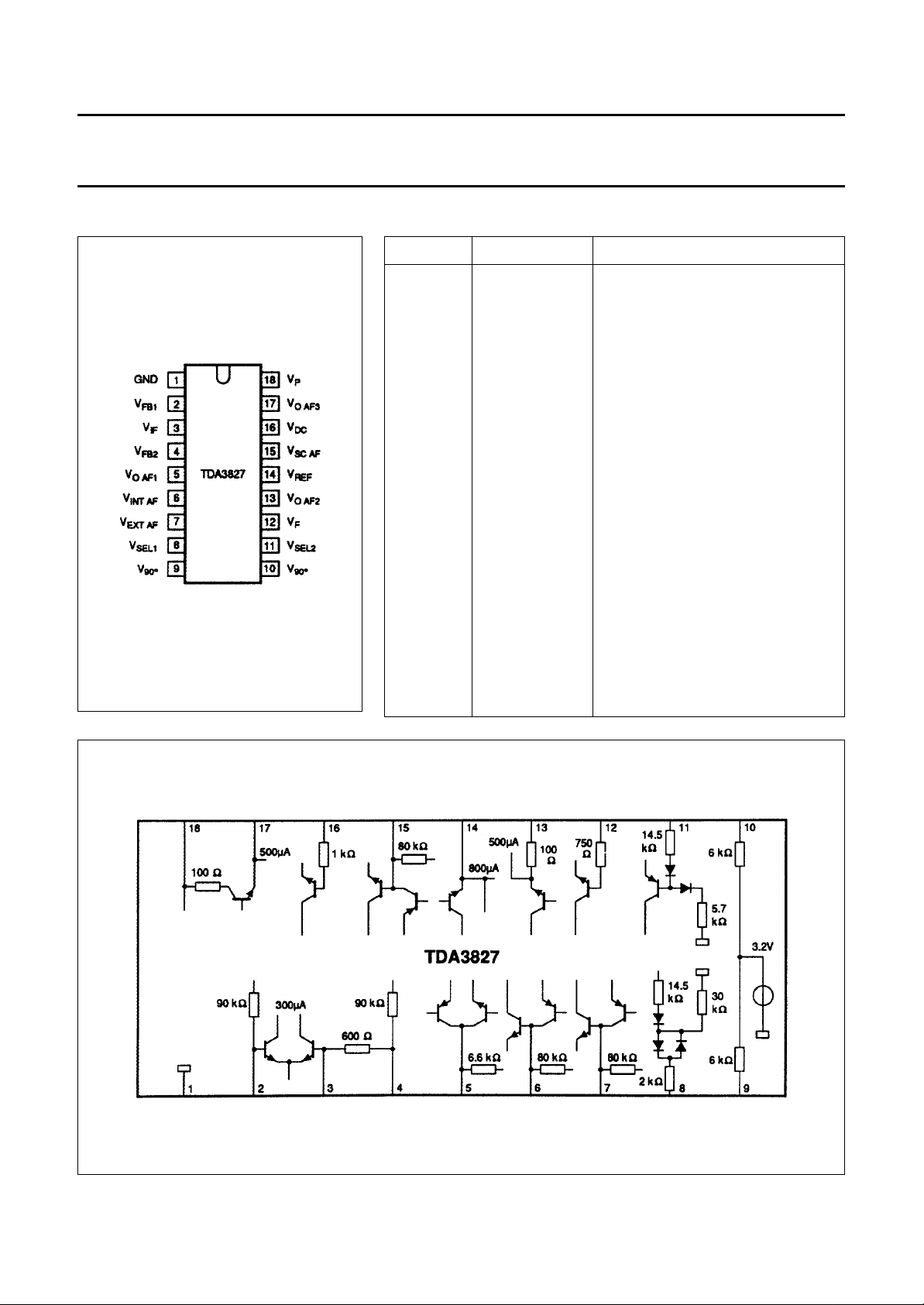
PIN CONFIGURATION
Fig.2 Pin configuration.
PINNING
SYMBOL PIN DESCRIPTION
GND 1 ground
V
FB1
V
IF
V
FB2
V
O AF1
V
INT AF
V
EXT AF
V
SEL1
V
90°
V
90°
V
SEL2
V
F
V
O AF2
V
REF
V
SC AF
V
DC
V
O AF3
V
P
TDA3827
2 limiter amplifier feedback
3 FM IF input signal
4 limiter amplifier feedback
5 AF output signal
6 internal AF input signal
7 external AF input signal
8 selection voltage for internal /
external AF input and mute
9
10
11 selection voltage for internal /
12 source selector feedback
13 output signal to SCART
14 reference voltage
15 input signal from SCART
16 DC volume control voltage
17 AF output signal from volume control
18 supply voltage
quadrature demodulator tuned
circuit reference
external or SCART audio
Fig.3 Internal circuits.
March 1991 4
Page 5

Philips Semiconductors Preliminary specification
TV-sound demodulator circuit with SCART
TDA3827
switches and AF control
LIMITING VALUES
In accordance with the Absolute Maximum System (IEC 134)
SYMBOL PARAMETER MIN. MAX. UNIT
V
P
V
ext
R
L
C
L
P
tot
T
stg
T
amb
V
ESD
Note to the limiting values
1. Measured with a 100 pF capacitor in series with a 1.5 kΩ resistor.
supply voltage (pin 18) −0.5 VP+ 6.8 V
external voltage (pins 2 to 10, 12 to 15 and 17) −0.3 VP− 0.7 V
external voltage at pin 11 −0.3 13.2 V
external voltage at pin 16 −0.3 V
P
V
external DC load resistance (pin 13 and pin 17) 5.0 − kΩ
capacitive output load (pin 13 and pin 17) − 1500 pF
total power dissipation − 450 mW
storage temperature range −40 + 150 °C
operating ambient temperature range 0 + 70 °C
ESD-protection (note 1) ±2000 − V
March 1991 5
Page 6

Philips Semiconductors Preliminary specification
TV-sound demodulator circuit with SCART
TDA3827
switches and AF control
CHARACTERISTICS
All voltages are measured to GND (pin 1); V
= 5 V; VIF = 10 mV; fo = 5.5 MHz; fAF = 1 kHz; ∆f = 50 kHz; T
P
measured in test circuit of Fig.4.; unless otherwise specified.
SYMBOL PARAMETER CONDITIONS MIN. TYP. MAX. UNIT
V
P
I
P
V
14
I
14
supply voltage.range (pin 18) 4.5 5.0 13.2 V
supply current (pin 18) VP = 5.0 V − 26 30 mA
= 12.0 V − 28 32 mA
V
P
reference voltage 2.2 2.3 2.4 V
output current −±250 −µA
IF limiting amplifier
V
i(rms)
input signal at pin 3
(RMS value)
3 dB below nominal AF
−−200 mV
− 30 50 µV
level at pin 5
R
3-1
V
2,3,4
FM demodulator (Q
V
5(rms)
input resistance − 600 −Ω
DC voltage − 2.1 − V
= 20)
L
AF-output signal (RMS value) 450 500 550 mV
residual 2f
-signal (RMS value) without de-emphasis −−30 mV
o
TC temperature coefficient (pin 5) − 1 2 mV/K
α
AM
AM suppression fAM = 400 Hz, m = 0.3,
V
= 500 µV; Fig.8
i(rms)
50 62 − dB
THD total harmonic distortion see Fig.8 − 0.3 0.5 %
Z
o
B
AF1
output impedance (pin 5) − 6.6 − kΩ
small signal bandwidth (pin 5) at −1 dB;
100 −− kHz
without de-emphasis
(S+N)/N signal to weighted noise ratio CCIR468-3, DIN45405;
73 78 − dB
see Fig.8
RR ripple rejection fR = 70 Hz,
VR = 100 mV
V
9,10
DC voltage − 3.2 − V
(p-p)
30 35 − dB
Source selector
V
i 6,7(rms)
Z
6,7
G
o
G
13/6,7
input signal (RMS value) − 500 1000 mV
input impedance 50 80 − kΩ
open loop gain − 60 − dB
gain see Fig.4 − 0 − dB
gain (typical application) see Fig.1 − 6 − dB
V
13
I
13
Z
13
C
L
V
13(rms)
DC voltage − 2.3 − V
DC output current −−1.0 mA
output impedance dynamic −−10 Ω
capacitive output load (pin 13) −−1500 pF
output signal (RMS value) handling THD < 0.1 % − 1.0 1.1 V
noise voltage (RMS value) B
= 20 kHz − 20 −µV
noise
= 25 °C;
amb
March 1991 6
Page 7

Philips Semiconductors Preliminary specification
TV-sound demodulator circuit with SCART
TDA3827
switches and AF control
SYMBOL PARAMETER CONDITIONS MIN. TYP. MAX. UNIT
B
AF2
dV/dt slew rate (pin 13) 1 −− V/µs
∆V
13
α
mute
α
7/6
Source selector control (see Fig.5)
V
8
I
8
V
8
I
8
V
8
I
8
SCART switch and level control
V
15(rms)
Z
15
G
17-15
G
max
∆G
V
V
17
I
17
Z
17
C
L
V
17(rms)
B
AF3
THD distortion (pin 17) at maximum gain − 0.5 1.0 %
∆V
17
V
16
I
16
α
6,7/15
small signal bandwidth at −1 dB 100 −− kHz
offset-voltage between any two
− 520 mV
source selector positions
AF suppression at mute 80 90 − dB
crosstalk attenuation 70 76 − dB
voltage for internal selection of
AF-input (pin 6)
1/3 V
P
− 2/3 V
−0.7
V
P
selection input current −−200 µA
voltage for external selection of
AF-input (pin 7)
2/3 V
+0.7
P
− V
P
V
selection input current 40 − 600 µA
voltage for mute active 0 − 1/3 Vp−1V
input current −10 −−500 µA
AC input signal (RMS value) − 500 1000 mV
input impedance 50 80 − kΩ
voltage gain V16 = 4.1 V −1.5 0 + 1.5 dB
maximum voltage gain V16 = 5.0 V + 4.0 + 5.0 + 6.0 dB
volume control range see Fig.7 80 86 − dB
DC voltage − 2.3 − V
DC output current −−−1mA
dynamic output impedance −−10 Ω
capacitive output load (pin 17) −−1500 pF
output signal (RMS value) THD ≤ 1% − 1.0 1.1 V
noise voltage (RMS value) B
= 20 kHz − 100 −µV
noise
small signal bandwidth (pin 17) at −3 dB 50 100 − kHz
offset voltage between internal and
− 520 mV
SCART
control voltage minimum gain −80 dB;
0.7 1.0 − V
see Fig.7
control current −−50 µA
crosstalk attenuation between
IF-stage and control-stage
IF sound modulated;
SCART switch on;
80 90 − dB
source-selector on
position input 1
March 1991 7
Page 8

Philips Semiconductors Preliminary specification
TV-sound demodulator circuit with SCART
TDA3827
switches and AF control
SYMBOL PARAMETER CONDITIONS MIN. TYP. MAX. UNIT
SCART switch control (see Fig.6)
V
I
11
V
I
11
11
11
voltage for internal active 0 − 4/5 VP−3V
current 0 −−100 µA
voltage for SCART active 4/5 VP−1 − 13.2 V
current − 700 µA
V111.4–
-----------------------
20.000
Fig.4 Test circuit.
March 1991 8
Page 9

Philips Semiconductors Preliminary specification
TV-sound demodulator circuit with SCART
switches and AF control
TDA3827
Fig.5 Source selector switching levels.
Fig.6 SCART switching levels.
March 1991 9
Page 10

Philips Semiconductors Preliminary specification
TV-sound demodulator circuit with SCART
switches and AF control
Fig.7 Volume control diagram.
TDA3827
Fig.8 AF output voltage at pin 5, THD, (S+N)/N in accordance with to CCIR468-3 and AM suppression αAM as
functions of IF input voltage VIF at pin 3.
March 1991 10
Page 11

Philips Semiconductors Preliminary specification
TV-sound demodulator circuit with SCART
switches and AF control
PACKAGE OUTLINE
DIP18: plastic dual in-line package; 18 leads (300 mil); slim corner leads
D
A
seating plane
L
Z
18
e
b
b
1
10
2
A
1
w M
b
2
TDA3827
SOT102-2
M
E
A
c
(e )
1
M
H
pin 1 index
1
0 5 10 mm
scale
DIMENSIONS (inch dimensions are derived from the original mm dimensions)
A
A
A
UNIT
max.
mm
inches
Note
1. Plastic or metal protrusions of 0.25 mm maximum per side are not included.
OUTLINE
VERSION
SOT102-2
12
min.
max.
IEC JEDEC EIAJ
b
1.40
1.14
0.055
0.045
b
1
0.53
0.38
0.021
0.015
b
2
0.32
1.05
0.23
0.75
0.013
0.041
0.009
0.030
REFERENCES
(1) (1)
cD E e M
21.8
21.4
0.86
0.84
9
6.48
6.20
0.26
0.24
E
(1)
Z
L
e
1
M
3.9
8.25
3.4
7.80
0.15
0.32
0.13
0.31
EUROPEAN
PROJECTION
E
0.37
0.33
H
9.5
8.3
w
max.
0.2542.54 7.62
0.854.7 0.51 3.7
0.010.10 0.30
0.0330.19 0.020 0.15
ISSUE DATE
93-10-14
95-01-23
March 1991 11
Page 12

Philips Semiconductors Preliminary specification
TV-sound demodulator circuit with SCART
TDA3827
switches and AF control
SOLDERING
Introduction
There is no soldering method that is ideal for all IC packages. Wave soldering is often preferred when through-hole and
surface mounted components are mixed on one printed-circuit board. However, wave soldering is not always suitable for
surface mounted ICs, or for printed-circuits with high population densities. In these situations reflow soldering is often
used.
This text gives a very brief insight to a complex technology. A more in-depth account of soldering ICs can be found in our
“IC Package Databook”
Soldering by dipping or by wave
The maximum permissible temperature of the solder is 260 °C; solder at this temperature must not be in contact with the
joint for more than 5 seconds. The total contact time of successive solder waves must not exceed 5 seconds.
The device may be mounted up to the seating plane, but the temperature of the plastic body must not exceed the
specified maximum storage temperature (T
be necessary immediately after soldering to keep the temperature within the permissible limit.
Repairing soldered joints
Apply a low voltage soldering iron (less than 24 V) to the lead(s) of the package, below the seating plane or not more
than 2 mm above it. If the temperature of the soldering iron bit is less than 300 °C it may remain in contact for up to
10 seconds. If the bit temperature is between 300 and 400 °C, contact may be up to 5 seconds.
(order code 9398 652 90011).
). If the printed-circuit board has been pre-heated, forced cooling may
stg max
DEFINITIONS
Data sheet status
Objective specification This data sheet contains target or goal specifications for product development.
Preliminary specification This data sheet contains preliminary data; supplementary data may be published later.
Product specification This data sheet contains final product specifications.
Limiting values
Limiting values given are in accordance with the Absolute Maximum Rating System (IEC 134). Stress above one or
more of the limiting values may cause permanent damage to the device. These are stress ratings only and operation
of the device at these or at any other conditions above those given in the Characteristics sections of the specification
is not implied. Exposure to limiting values for extended periods may affect device reliability.
Application information
Where application information is given, it is advisory and does not form part of the specification.
LIFE SUPPORT APPLICATIONS
These products are not designed for use in life support appliances, devices, or systems where malfunction of these
products can reasonably be expected to result in personal injury. Philips customers using or selling these products for
use in such applications do so at their own risk and agree to fully indemnify Philips for any damages resulting from such
improper use or sale.
March 1991 12
 Loading...