

Page 1

INTEGRATED CIRCUITS
DATA SH EET
TDA3654
TDA3654Q
Vertical deflection and guard circuit
(110˚)
Product specification
File under Integrated Circuits, IC02
March 1991
Page 2

Philips Semiconductors Product specification
Vertical deflection and guard circuit
(110˚)
TDA3654
TDA3654Q
GENERAL DESCRIPTION
The TDA3654 is a full performance vertical deflection output circuit for direct drive of the deflection coils and can be used
for a wide range of 90° and 110° deflection systems.
A guard circuit is provided which blanks the picture tube screen in the absence of deflection current.
Features
• Direct drive to the deflection coils
• 90° and 110° deflection system
• Internal blanking guard circuit
• Internal voltage stabilizer
QUICK REFERENCE DATA
Output voltage V
Output current (peak-to-peak) I
Supply voltage V
Guard circuit output voltage V
Operating ambient temperature range T
Storage temperature T
5-2
5(p-p)
9-2
7-2
amb
stg
max. 60 V
max. 3 A
max. 40 V
max. 5,6 V
−25 to +60 °C
−55 to +150 °C
THERMAL RESISTANCE
From junction to mounting base R
PACKAGE OUTLINES
(1)
TDA3654 : 9-lead SIL; plastic power (SOT131)
TDA3654Q : 9-lead SIL bent to DIL; plastic power (SOT157)
.
(2)
.
Notes
1. SOT131-2; 1997 January 07
2. SOT157-2; 1997 January 07
th j-mb
3,5 to 4 K/W
March 1991 2
Page 3
Philips Semiconductors Product specification
Vertical deflection and guard circuit (110˚)
TDA3654
TDA3654Q
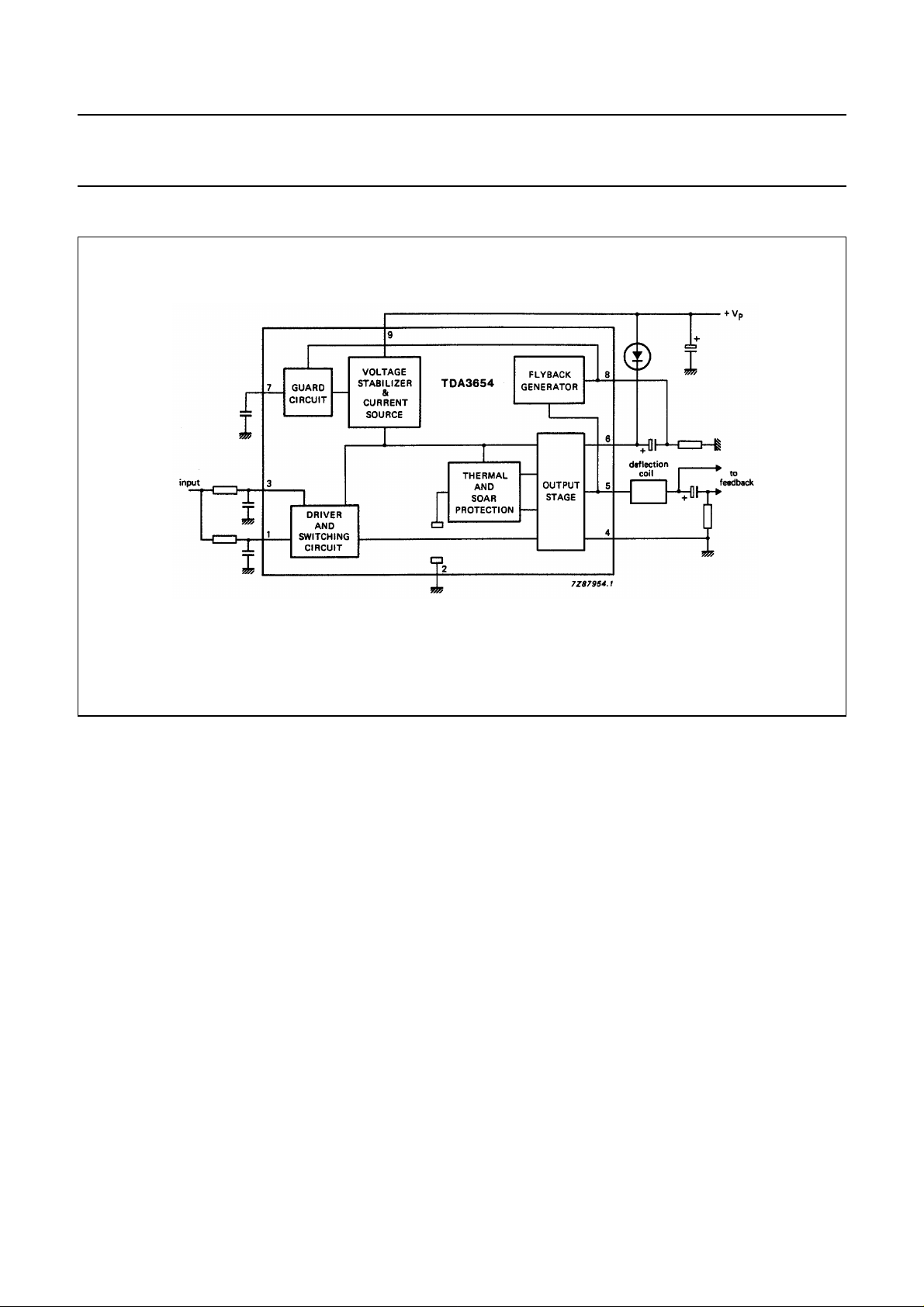
Fig.1 Block diagram.
March 1991 3
Page 4

Philips Semiconductors Product specification
Vertical deflection and guard circuit (110˚)
TDA3654
TDA3654Q
FUNCTIONAL DESCRIPTION
Output stage and protection circuits
The output stage consists of two Darlington configurations in class B arrangement.
Each output transistor can deliver 1,5 A maximum and the V
Protection of the output stage is such that the operation of the transistors remains well within the SOAR area in all
circumstances at the output pin, (pin 5). This is obtained by the cooperation of the thermal protection circuit, the
current-voltage detector and the short circuit protection.
Special measures in the internal circuit layout give the output transistors extra solidity, this is illustrated in Fig.5 where
typical SOAR curves of the lower output transistor are given. The same curves also apply for the upper output device.
The supply for the output stage is fed to pin 6 and the output stage ground is connected to pin 4.
Driver and switching circuit
Pin 1 is the input for the driver of the output stage. The signal at pin 1 is also applied to pin 3 which is the input of a
switching circuit (pin 1 and 3 are connected via external resistors).
This switching circuit rapidly turns off the lower output stage when the flyback starts and it, therefore, allows a quick start
of the flyback generator. The maximum required input signal for the maximum output current peak-to-peak value of 3 A
is only 3 V, the sum of the currents in pins 1 and 3 is then maximum 1 mA.
Flyback generator
CEO
is 60 V.
During scan, the capacitor between pins 6 and 8 is charged to a level which is dependent on the value of the resistor at
pin 8 (see Fig.1).
When the flyback starts and the voltage at the output pin (pin 5) exceeds the supply voltage, the flyback generator is
activated.
The supply voltage is then connected in series, via pin 8, with the voltage across the capacitor during the flyback period.
This implies that during scan the supply voltage can be reduced to the required scan voltage plus saturation voltage of
the output transistors.
The amplitude of the flyback voltage can be chosen by changing the value of the external resistor at pin 8.
It should be noted that the application is chosen such that the lowest voltage at pin 8 is > 1,5 V, during normal operation.
Guard circuit
When there is no deflection current, for any reason, the voltage at pin 8 becomes less than 1 V, the guard circuit will
produce a d.c. voltage at pin 7. This voltage can be used to blank the picture tube, so that the screen will not burn in.
Voltage stabilizer
The internal voltage stabilizer provides a stabilized supply of 6 V to drive the output stage, so the drive current is not
affected by supply voltage variations.
March 1991 4
Page 5

Philips Semiconductors Product specification
Vertical deflection and guard circuit (110˚)
RATINGS
Limiting values in accordance with the Absolute Maximum System (IEC 134).
Pins 2 and 4 are externally connected to ground.
Voltages
Output voltage V
Supply voltage V
Supply voltage output stage V
Input voltage V
Input voltage switching circuit V
External voltage at pin 7 V
Currents
Repetitive peak output current ± I
Non-repetitive peak output current (note 1) ± I
Repetitive peak output current of flyback generator I
Non-repetitive peak output current of flyback generator (note 1) ± I
Temperatures
Storage temperature range T
Operating ambient temperature range (see Fig.3) T
Operating junction temperature range T
(the output current at pin 5 should not exceed 2.5A)
5-4
9-4
6-4
1-2
3-2
7-2
8RM
stg
amb
j
5RM
5SM
8SM
TDA3654
TDA3654Q
0 to 60 V
0 to 40 V
0 to 60 V
0 to V
0 to V
0 to 5,6 V
max. 1,5 A
max. 3 A
max. + 1,5 A
− 1,6 A
max. 3 A
−65 to + 150 °C
−25 to + 60 °C
−25 to + 150 °C
9-4
9-4
V
V
March 1991 5
Page 6

Philips Semiconductors Product specification
Vertical deflection and guard circuit (110˚)
TDA3654
TDA3654Q
CHARACTERISTICS
=25°C, supply voltage (V
T
amb
Pins 2 and 4 externally connected to ground.
PARAMETER SYMBOL MIN. TYP. MAX. UNIT
Supply
Supply voltage, pin 9 (note 2) V
Supply voltage output stage V
Supply current, pins
6 and 9 (note 3) I
Quiescent current (note 4) I
Variation of quiescent current
with temperature TC −−0,04 − mA/K
Output current
Output current, pin 5
(peak-to-peak) I
Output current flyback
generator, pin 8 + I
Output voltage
Peak voltage during flyback V
Saturation voltage to supply
at I5= −1,5 A V
at I
= 1,5 A (note 5) V
5
= −1,2 A V
at I
5
at I
= 1,2 A (note 5) V
5
Saturation voltage to ground
at I
= 1,2 A V
5
at I
= 1,5 A V
5
Flyback generator
Saturation voltage
= −1,6 A V
at I
8
at I
= 1,5 A (note 5) V
8
at I
= −1,3 A V
8
at I
= 1,2 A (note 5) V
8
Leakage current at pin 8 −I
Flyback generator active if: V
Input
Input current, pin 1,
for I
= 1,5 A I
5
Input voltage during scan, pin 1 V
) = 26 V; unless otherwise stated; pin 1 externally connected to pin 3.
9-4
9-4
6-4
6+I9
4
5(p-p)
−I
8(p-p)
5-4
6-5(sat)
5-6(sat)
6-5(sat)
5-6(sat)
5-4(sat)
5-4(sat)
9-8(sat)
8-9(sat)
9-8(sat)
8-9(sat)
8
5-9
1
1-2
8(p-p)
10 − 40 V
−−60 V
35 55 85 mA
25 40 65 mA
− 2,5 3 A
− 1,25 1,5 A
− 1,35 1,6 A
−−60 V
2,5 3,2 V
2,5 3,2 V
2,2 2,7 V
2,3 2,8 V
− 2,2 2,7 V
− 2,5 3,2 V
− 1,6 2,1 V
− 2,3 3 V
− 1,4 1,9 V
− 2,2 2,7 V
− 5 100 µA
4 −− V
− 0,33 0,55 mA
− 2,35 3 V
March 1991 6
Page 7

Philips Semiconductors Product specification
Vertical deflection and guard circuit (110˚)
TDA3654
TDA3654Q
PARAMETER SYMBOL MIN. TYP. MAX. UNIT
Input current, pin 3,
during scan (note 6) I
3
Input voltage, pin 3,
during scan (note 6) V
3-2
Input voltage, pin 1,
during flyback V
1-2
Input voltage, pin 3,
during flyback V
3-2
Guard circuit
Output voltage, pin 7
R
= 100 kΩ (note 9) V
L
7-2
Output voltage, pin 7 at
I
= 0,5 mA (note 9) V
L
7-2
Internal series resistance
of pin 7 Ri
7
Guard circuit activates
(note 7) V
8-2
General data
Thermal protection activation
range T
j
Thermal resistance
From junction to mounting base R
Power dissipation P
th j-mb
tot
Open loop gain at
1 kHz; (note 8) G
o
Frequency response,
−3 dB; (note 10) f − 60 − kHz
0,03 −− mA
0,8 − V
9-4
−−250 mV
−−250 mV
4,1 4,5 5,8 V
3,4 3,9 5,3 V
0,95 1,35 1,7 kΩ
−−1,0 V
158 175 192 °C
− 3,5 4 K/W
− see Fig.3
− 33 −
V
Notes
1. Non-repetitive duty factor 3,3%.
2. The maximum supply voltage should be chosen so that during flyback the voltage at pin 5 does not exceed 60 V.
3. When V
is 13 V and no load at pin 5.
5-4
4. See Fig.4.
5. Duty cycle, d = 5% or d = 0,05.
6. When pin 3 is driven separately from pin 1.
7. During normal operation the voltage V
may not be lower than 1,5 V.
8-2
8. RL=8Ω; IL= 125 mA (r.m.s.).
9. If guard circuit is active.
10. With a 22 pF capacitor between pins 1 and 5.
March 1991 7
Page 8

Philips Semiconductors Product specification
Vertical deflection and guard circuit (110˚)
TDA3654
TDA3654Q
Fig.2 Application diagram.
March 1991 8
Page 9

Philips Semiconductors Product specification
Vertical deflection and guard circuit (110˚)
TDA3654
TDA3654Q
Fig.3 Power derating curve.
Fig.4 Quiescent current as a function of the supply voltage.
March 1991 9
Page 10

Philips Semiconductors Product specification
Vertical deflection and guard circuit (110˚)
peak
curve t
1 d.c. − 150 °C
2 10 ms 0,5 150 °C
3 10 ms 0,25 150 °C
4 1 ms 0,5 150 °C
5 1 ms 0,25 150 °C
6 1 ms 0,05 150 °C
7 1 ms 0,05 180 °C
8 0,2 ms 0,1 150 °C
9 0,2 ms 0,1 180 °C
p
δ
junction
temperature
TDA3654
TDA3654Q
Fig.5 Typical SOAR of lower output transistor.
March 1991 10
Page 11

Philips Semiconductors Product specification
Vertical deflection and guard circuit (110˚)
TDA3654
TDA3654Q
Fig.6 Application diagram in combination with TDA2579.
March 1991 11
Page 12

Philips Semiconductors Product specification
Vertical deflection and guard circuit (110˚)
PACKAGE OUTLINES
SIL9P: plastic single in-line power package; 9 leads
D
d
j
TDA3654Q
non-concave
x
E
h
view B: mounting base side
A
B
D
h
2
E
TDA3654
SOT131-2
seating plane
b
19
Z
DIMENSIONS (mm are the original dimensions)
A
UNIT A
mm
Note
1. Plastic or metal protrusions of 0.25 mm maximum per side are not included.
1
max.
2.0
OUTLINE
VERSION
SOT131-2
4.6
4.2
e
b
b
cD
max.
1.1
p2
0.75
0.48
0.60
0.38
IEC JEDEC EIAJ
b
p
(1)
24.0
23.6
REFERENCES
w M
0 5 10 mm
scale
deD
h
20.0
10 2.54
19.6
E
12.2
11.8
A
1
L
c
Q
(1)
E
h
6
3.4
3.1
Lj
Q
17.2
2.1
16.5
1.8
EUROPEAN
PROJECTION
0.25w0.03
ISSUE DATE
92-11-17
95-03-11
(1)
Z
x
2.00
1.45
March 1991 12
Page 13

Philips Semiconductors Product specification
Vertical deflection and guard circuit (110˚)
DBS9P: plastic DIL-bent-SIL power package; 9 leads (lead length 12 mm)
non-concave
D
d
x
E
h
D
h
view B: mounting base side
A
2
TDA3654
TDA3654Q
SOT157-2
j
19
e
0.75
0.60
1
e
cD
0.48
24.0
0.38
23.6
(1)
deD
20.0
19.6
Z
DIMENSIONS (mm are the original dimensions)
UNIT A A e
17.0
15.5
4.6
4.2
mm
Note
1. Plastic or metal protrusions of 0.25 mm maximum per side are not included.
w M
b
p
E
h
12.2
10 5.08
11.8
0 5 10 mm
scale
(1)
12bp
2.54
e
5.08
B
E
A
L
3
L
E
2
h
6
Q
LL3m
3.4
12.4
3.1
11.0
c
2.4
1.6
e
4.3
2.1
1.8
v M
(1)
v
Qj
0.8
0.25w0.03
Z
x
2.00
1.45
2
m
OUTLINE
VERSION
SOT157-2
IEC JEDEC EIAJ
REFERENCES
March 1991 13
EUROPEAN
PROJECTION
ISSUE DATE
92-10-12
95-03-11
Page 14

Philips Semiconductors Product specification
Vertical deflection and guard circuit (110˚)
TDA3654
TDA3654Q
SOLDERING
Introduction
There is no soldering method that is ideal for all IC packages. Wave soldering is often preferred when through-hole and
surface mounted components are mixed on one printed-circuit board. However, wave soldering is not always suitable for
surface mounted ICs, or for printed-circuits with high population densities. In these situations reflow soldering is often
used.
This text gives a very brief insight to a complex technology. A more in-depth account of soldering ICs can be found in our
“IC Package Databook”
Soldering by dipping or by wave
The maximum permissible temperature of the solder is 260 °C; solder at this temperature must not be in contact with the
joint for more than 5 seconds. The total contact time of successive solder waves must not exceed 5 seconds.
The device may be mounted up to the seating plane, but the temperature of the plastic body must not exceed the
specified maximum storage temperature (T
be necessary immediately after soldering to keep the temperature within the permissible limit.
Repairing soldered joints
Apply a low voltage soldering iron (less than 24 V) to the lead(s) of the package, below the seating plane or not more
than 2 mm above it. If the temperature of the soldering iron bit is less than 300 °C it may remain in contact for up to
10 seconds. If the bit temperature is between 300 and 400 °C, contact may be up to 5 seconds.
(order code 9398 652 90011).
). If the printed-circuit board has been pre-heated, forced cooling may
stg max
DEFINITIONS
Data sheet status
Objective specification This data sheet contains target or goal specifications for product development.
Preliminary specification This data sheet contains preliminary data; supplementary data may be published later.
Product specification This data sheet contains final product specifications.
Short-form specification The data in this specification is extracted from a full data sheet with the same type
number and title. For detailed information see the relevant data sheet or data handbook.
Limiting values
Limiting values given are in accordance with the Absolute Maximum Rating System (IEC 134). Stress above one or
more of the limiting values may cause permanent damage to the device. These are stress ratings only and operation
of the device at these or at any other conditions above those given in the Characteristics sections of the specification
is not implied. Exposure to limiting values for extended periods may affect device reliability.
Application information
Where application information is given, it is advisory and does not form part of the specification.
LIFE SUPPORT APPLICATIONS
These products are not designed for use in life support appliances, devices, or systems where malfunction of these
products can reasonably be expected to result in personal injury. Philips customers using or selling these products for
use in such applications do so at their own risk and agree to fully indemnify Philips for any damages resulting from such
improper use or sale.
March 1991 14
Page 15

 Loading...