

Page 1
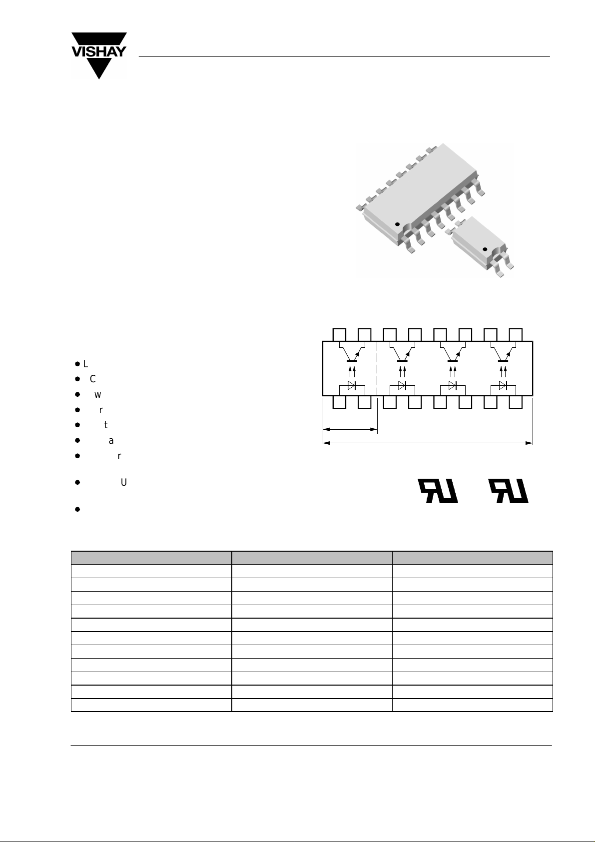
TCMT11.. Series
Optocoupler with Phototransistor Output
Description
The TCMT11.. Series consist of a phototransistor
optically coupled to a gallium arsenide infraredemitting diode in an 4- lead up to 16- lead plastic
Miniflat package.
The elements are mounted on one leadframe using a
coplanar technique, providing a fixed distance
between input and output for highest safety
requirements.
Applications
Programmable logic controllers, modems, answering
machines, general applications
Coll. Emitter
Features
Vishay Semiconductors
16467
9
D
Low profile package (half pitch)
D
AC Isolation test voltage V
D
Low coupling capacitance of typical 0.3 pF
D
Current Transfer Ratio (CTR) selected into groups
D
Low temperature coefficient of CTR
D
Wide ambient temperature range
D
Underwriters Laboratory (UL) 1577 recognized,
file number E-76222
D
CSA (C-UL) 1577 recognized
file number E- 76222 - Double Protection
D
Coupling System M
= 3.75 kV
io
RMS
12 8
Anode Cath.
4 PIN
16 PIN
C
Order Instruction
Ordering Code CTR Ranking Remarks
TCMT1 100 50 to 600% 4 Pin = Single channel
TCMT1101 40 to 80% 4 Pin = Single channel
TCMT1102 63 to 125% 4 Pin = Single channel
TCMT1103 100 to 200% 4 Pin = Single channel
TCMT1104 160 to 320% 4 Pin = Single channel
TCMT1105 50 to 150% 4 Pin = Single channel
TCMT1106 100 to 300% 4 Pin = Single channel
TCMT1107 80 to 160% 4 Pin = Single channel
TCMT1108 130 to 260% 4 Pin = Single channel
TCMT1109 200 to 400% 4 Pin = Single channel
TCMT4100 50 to 600% 16 Pin = Quad channel
16281
Rev. A2, 15–Dec–00
www.vishay.comDocument Number 83510
1 (12)
Page 2
TCMT11.. Series
Vishay Semiconductors
Absolute Maximum Ratings
Input (Emitter)
Parameter Test Conditions Symbol Value Unit
Reverse voltage V
Forward current I
Forward surge current tp ≤ 10 ms I
Power dissipation T
Junction temperature T
Output (Detector)
Parameter Test Conditions Symbol Value Unit
Collector emitter voltage V
Emitter collector voltage V
Collector current I
Peak collector current tp/T = 0.5, tp ≤ 10 ms I
Power dissipation T
Junction temperature T
≤ 25°C P
amb
≤ 25°C P
amb
R
F
FSM
V
CEO
ECO
C
CM
V
6 V
60 mA
1.5 A
100 mW
j
125
°
C
70 V
7 V
50 mA
100 mA
150 mW
j
125
°
C
Coupler
Parameter Test Conditions Symbol V alue Unit
AC isolation test voltage (RMS) VIO
Total power dissipation T
Operating ambient temperature
range
Storage temperature range T
Soldering temperature T
1)
Related to standard climate 23/50 DIN 50014
≤ 25°C P
amb
T
tot
amb
stg
sd
1)
3.75 kV
250 mW
–40 to +100
–40 to +100
235
°
C
°
C
°
C
www.vishay.com
2 (12) Rev. A2, 15–Dec–00
Document Number 83510
Page 3
TCMT11.. Series
C F
Vishay Semiconductors
Electrical Characteristics (T
amb
= 25°C)
Input (Emitter)
Parameter Test Conditions Symbol Min. Typ. Max. Unit
Forward voltage IF = 50 mA V
Junction capacitance VR = 0 V, f = 1 MHz C
Output (Detector)
Parameter Test Conditions Symbol Min. Typ. Max. Unit
Collector emitter voltage IC = 100 mA V
Emitter collector voltage IE = 100 mA V
Collector dark current VCE = 20 V, IF = 0, E = 0 I
Coupler
Parameter Test Conditions Symbol Min. Typ. Max. Unit
Collector emitter saturation
voltage
Cut-off frequency IF = 10 mA, VCE = 5 V,
Coupling capacitance f = 1 MHz C
IF = 10 mA, IC = 1 mA V
RL = 100
W
F
j
CEO
ECO
CEO
CEsat
f
c
k
1.25 1.6 V
50 pF
70 V
7 V
100 nA
0.3 V
100 kHz
0.3 pF
Current Transfer Ratio (CTR)
Parameter Test Conditions Type Symbol Min. Typ. Max. Unit
IC/I
F
VCE = 5 V, IF = 5 mA TCMT1100 CTR 0.5 6.0
VCE = 5 V, IF = 10 mA TCMT1101 CTR 0.4 0.8
VCE = 5 V, IF = 10 mA TCMT1102 CTR 0.63 1.25
VCE = 5 V, IF = 10 mA TCMT1103 CTR 1.0 2.0
VCE = 5 V, IF = 10 mA TCMT1104 CTR 1.6 3.2
VCE = 5 V, IF = 5 mA TCMT1105 CTR 0.5 1.5
VCE = 5 V, IF = 5 mA TCMT1106 CTR 1.0 3.0
VCE = 5 V, IF = 5 mA TCMT1107 CTR 0.8 1.6
VCE = 5 V, IF = 5 mA TCMT1108 CTR 1.3 2.6
VCE = 5 V, IF = 5 mA TCMT1109 CTR 2.0 4.0
VCE = 5 V, IF = 5 mA TCMT4100 CTR 0.5 6.0
Rev. A2, 15–Dec–00
www.vishay.comDocument Number 83510
3 (12)
Page 4
TCMT11.. Series
S C L
(g)
S F L
(g)
Vishay Semiconductors
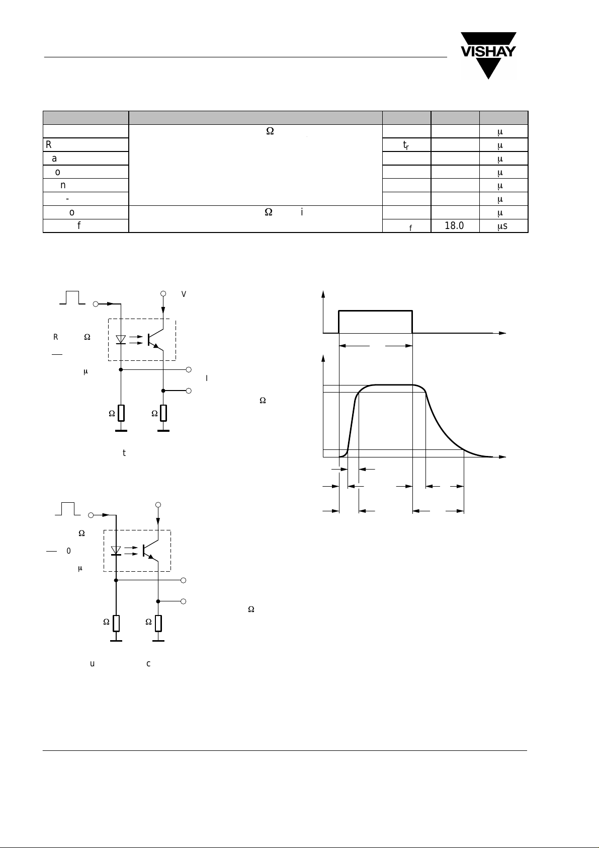
Switching Characteristics
Parameter T est Conditions Symbol T yp. Unit
Delay time VS = 5 V, IC = 2 mA, RL = 100 W (see figure 1) t
Rise time
Fall time t
Storage time t
Turn-on time t
Turn-off time t
Turn-on time VS = 5 V, IF = 10 mA, RL = 1 kW (see figure 2) t
Turn-off time
d
t
r
f
s
on
off
on
t
off
3.0
3.0
4.7
0.3
6.0
5.0
9.0
18.0
m
s
m
s
m
s
m
s
m
s
m
s
m
s
m
s
W
+ 5 V
= 2 mA;
I
C
Channel I
Channel II
0
R
G
t
p
T
t
p
95 10804
I
F
= 50 W
= 0.01
= 50 ms
50
I
F
W
100
Figure 1. Test circuit, non-saturated operation
W
+ 5 V
I
C
Channel I
Channel II
0
R
= 50 W
G
t
p
= 0.01
T
t
= 50 ms
p
95 10843
I
F
IF = 10 mA
50
W
1 k
adjusted through
input amplitude
Oscilloscope
R
= 1 M
W
L
C
= 20 pF
L
Oscilloscope
> 1 M
R
CL < 20 pF
W
L
I
F
0
I
C
100%
90%
10%
0
t
r
t
d
t
on
t
p
t
d
t
r
t
(= td + tr) turn-on time
on
pulse duration
delay time
rise time
Figure 3. Switching times
96 11698
t
p
t
t
s
f
t
off
t
s
t
f
t
(= ts + tf) turn-off time
off
t
t
storage time
fall time
Figure 2. Test circuit, saturated operation
www.vishay.com
4 (12) Rev. A2, 15–Dec–00
Document Number 83510
Page 5

TCMT11.. Series
Vishay Semiconductors
Typical Characteristics (T
300
Coupled device
250
200
Phototransistor
150
IR-diode
100
50
tot
P – Total Power Dissipation ( mW )
0
0 40 80 120
T
– Ambient Temperature ( °C )96 11700
amb
Figure 4. Total Power Dissipation vs.
Ambient Temperature
1000.0
100.0
= 25_C, unless otherwise specified)
amb
10000
VCE=20V
I
=0
1000
100
with open Base ( nA )
CEO
I – Collector Dark Current,
95 11026
F
10
1
0255075
T
– Ambient Temperature ( °C )
amb
Figure 7. Collector Dark Current vs. Ambient Temperature
100
VCE=5V
10
100
10.0
1.0
F
I – Forward Current ( mA )
0.1
0 0.2 0.4 0.6 0.8 1.0 1.2 1.4 1.6 1.8 2.0
VF – Forward Voltage ( V )96 11862
Figure 5. Forward Current vs. Forward Voltage
2.0
V
=5V
CE
I
=5mA
1.5
1.0
0.5
rel
CTR – Relative Current Transfer Ratio
0
–25 0 25 50
T
– Ambient Temperature ( °C )95 11025
amb
F
75
1
0.1
C
I – Collector Current ( mA )
0.01
0.1 1 10
95 11027
IF – Forward Current ( mA )
Figure 8. Collector Current vs. Forward Current
100
20mA
IF=50mA
10mA
5mA
2mA
1mA
C
I – Collector Current ( mA )
95 10985
10
1
0.1
0.1 1 10
V
– Collector Emitter Voltage ( V )
CE
100
100
Figure 6. Relative Current Transfer Ratio vs.
Ambient Temperature
Rev. A2, 15–Dec–00
Figure 9. Collector Current vs. Collector Emitter Voltage
www.vishay.comDocument Number 83510
5 (12)
Page 6

TCMT11.. Series
)
Vishay Semiconductors
1.0
20%
0.8
CTR=50%
0.6
0.4
CEsat
V – Collector Emitter Saturation Voltage ( V
95 11028
0.2
0
110
IC – Collector Current ( mA )
10%
100
Figure 10. Collector Emitter Saturation Voltage vs.
Collector Current
1000
VCE=5V
100
10
50
m
off
on
t / t – Turn on / Turn off Time ( s )
95 11031
Saturated Operation
V
=5V
40
30
20
10
0
S
R
=1k
W
L
0 5 10 15
I
– Forward Current ( mA )
F
t
off
t
on
20
Figure 12. Turn on / off Time vs. Forward Current
10
m
8
t
on
6
t
off
4
Non Saturated
Operation
V
=5V
S
R
=100
W
L
2
CTR – Current Transfer Ratio ( % )
95 11029
1
0.1 1 10
IF – Forward Current ( mA )
100
Figure 11. Current Transfer Ratio vs. Forward Current
Pin 1 Indication T ype
off
on
t / t – Turn on / Turn off Time ( s )
95 11030
0
02 4 6
I
– Collector Current ( mA )
C
10
Figure 13. Turn on / off Time vs. Collector Current
System Letter
T1100M
901TK27
15230
Date
Code
(YM)
Company
Logo
Production
Location
Figure 14. Marking example
www.vishay.com
6 (12) Rev. A2, 15–Dec–00
Document Number 83510
Page 7

Dimensions of TCMT1... in mm
TCMT11.. Series
Vishay Semiconductors
Rev. A2, 15–Dec–00
16283
www.vishay.comDocument Number 83510
7 (12)
Page 8

TCMT11.. Series
Vishay Semiconductors
Dimensions of TCMT4... in mm
15226
www.vishay.com
8 (12) Rev. A2, 15–Dec–00
Document Number 83510
Page 9

Dimensions of Reel in mm
TCMT11.. Series
Vishay Semiconductors
W
1
N
A
Reel Hub
W
2
Version Tape Width A N W
G 16 330 ± 1 100 ± 1.5 16.4 + 2 22.4
Dimensions of Leader and Trailer in mm
Trailer Leader
no devices no devices
min. 200 min. 400
devices
16515
1
W
2 max
StartEnd
96 11818
Rev. A2, 15–Dec–00
www.vishay.comDocument Number 83510
9 (12)
Page 10

TCMT11.. Series
Vishay Semiconductors
Dimensions of Tape in mm
16511
www.vishay.com
10 (12) Rev. A2, 15–Dec–00
Document Number 83510
Page 11

Dimensions of Tape in mm
TCMT11.. Series
Vishay Semiconductors
Rev. A2, 15–Dec–00
16510
www.vishay.comDocument Number 83510
11 (12)
Page 12

TCMT11.. Series
Vishay Semiconductors
Ozone Depleting Substances Policy Statement
It is the policy of Vishay Semiconductor GmbH to
1. Meet all present and future national and international statutory requirements.
2. Regularly and continuously improve the performance of our products, processes, distribution and operating
systems with respect to their impact on the health and safety of our employees and the public, as well as
their impact on the environment.
It is particular concern to control or eliminate releases of those substances into the atmosphere which are known as
ozone depleting substances (ODSs).
The Montreal Protocol (1987) and its London Amendments (1990) intend to severely restrict the use of ODSs and
forbid their use within the next ten years. V arious national and international initiatives are pressing for an earlier ban
on these substances.
Vishay Semiconductor GmbH has been able to use its policy of continuous improvements to eliminate the use of
ODSs listed in the following documents.
1. Annex A, B and list of transitional substances of the Montreal Protocol and the London Amendments respectively
2. Class I and II ozone depleting substances in the Clean Air Act Amendments of 1990 by the Environmental
Protection Agency (EPA) in the USA
3. Council Decision 88/540/EEC and 91/690/EEC Annex A, B and C (transitional substances) respectively.
Vishay Semiconductor GmbH can certify that our semiconductors are not manufactured with ozone depleting
substances and do not contain such substances.
We reserve the right to make changes to improve technical design and may do so without further notice.
Parameters can vary in different applications. All operating parameters must be validated for each customer application
by the customer. Should the buyer use Vishay Semiconductors products for any unintended or unauthorized application, the
buyer shall indemnify Vishay Semiconductors against all claims, costs, damages, and expenses, arising out of, directly or
indirectly , any claim of personal damage, injury or death associated with such unintended or unauthorized use.
Vishay Semiconductor GmbH, P.O.B. 3535, D-74025 Heilbronn, Germany
Telephone: 49 (0)7131 67 2831, Fax number: 49 (0)7131 67 2423
www.vishay.com
12 (12) Rev. A2, 15–Dec–00
Document Number 83510
 Loading...