

Datasheet TCM853EOA, TCM853COA, TCM852EOA, TCM852COA, TCM851COA Datasheet (TelCom Semiconductor)
...Page 1
REGULATED GaAs FET BIAS SUPPLY
EVALUATION
KIT
AVAILABLE
TCM850
TCM851
TCM852
TCM853
1
FEATURES
■ Fixed – 4.1V or Adjustable – 0.5V to – 9V Output
at 5mA
■ 4.5V to 10V Input Voltage Range
■ Low Output Voltage Ripple
TCM850-852 ..............................................2mVp-p
TCM853......................................................1mVp-p
■ 100kHz Charge Pump Switching Frequency
■ Optional External Synchronizing Clock
Input (TCM852)
■ Logic Level Shutdown Mode ................ 0.5µA Typ.
Temperature (TCM850/852/853)
■ Low Cost, 8-Pin SOIC Package
APPLICATIONS
■ Cellular Phones
■ Negative Regulated Power Supplies
■ LCD Bias Contrast Control
■ Adjustable GaAs FET Bias
■ Wireless Data Loggers
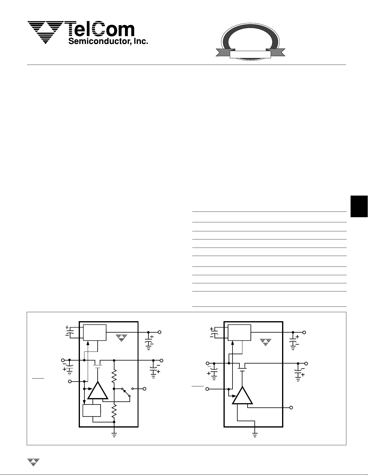
FUNCTIONAL BLOCK DIAGRAM
GENERAL DESCRIPTION
The TCM850/1/2/3 combines an inverting charge pump
and a low noise linear regulator in a single small outline
package. They are ideal for biasing GaAS FETs in cellular
telephone transmitter power amplifiers
All four devices accept a range of input voltages from
4.5V to 10.0V and have – 5mA output current capability. The
TCM850/1/2 have both preset (– 4.1V) and variable (– 0.5V
to –9.0V) output voltages that program with an external
resistor divider. The TCM853 output voltage programs with
an external positive control voltage. The TCM850/1/3 can
be shutdown reducing quiescent current to less than
0.5µA (typ) over temperature, 2µA (typ) for the TCM851.
ORDERING INFORMATION
Part No. Package Temp. Range
TCM850COA 8-Pin SOIC 0°C to +70°C
TCM850EOA 8-Pin SOIC – 40°C to +85°C
TCM851COA 8-Pin SOIC 0°C to +70°C
TCM851EOA 8-Pin SOIC – 40°C to +85°C
TCM852COA 8-Pin SOIC 0°C to +70°C
TCM852EOA 8-Pin SOIC – 40°C to +85°C
TCM853COA 8-Pin SOIC 0°C to +70°C
TCM853EOA 8-Pin SOIC – 40°C to +85°C
TCM850EV Evaluation Kit for
TCM850/1/2/3
2
3
4
5
NEGOUT
SHDN (TCM850)
SHDN (TCM851)
OSC (TCM852)
TELCOM SEMICONDUCTOR, INC.
+
C1
C1
–
CHARGE
PUMP
N
+
– 1.28V
REF
–
TCM850
TCM851
TCM852
GND
IN
C
3
OUT
C4
FB
(GND to SET
= – 4.1V)
V
OUT
C
SHDN
Figure 1.
C
1
C
2
+
C1
C1
–
CHARGE
PUMP
N
TCM853
IN
C
3
OUTNEGOUT
C
4
C
1
2
6
7
+
–
CONT
(CONTROL VOLTAGE)
GND
TC850/1/2/3-3 10/1/96
4-27
8
Page 2
TCM850
TCM851
TCM852
TCM853
REGULATED GaAs FET BIAS SUPPLY
ABSOLUTE MAXIMUM RATINGS*
Supply Voltage (V
V
NEGOUT
VIN to V
V
OUT
to GND ...................................... – 10.5V to 0.3V
NEGOUT
to GND** ........................................ V
SHDN or OSC (Pin 4) to GND ........– 0.3V to (V
to GND).................. – 0.3V to +10.5V
IN
...............................................................– 0.3 to 21V
NEGOUT
to 0.3V
+ 0.3V)
IN
*This is a stress ratings only and functional operation of the device at these
or any other conditions above those indicated in the operational sections of
the specifications is not implied. Exposure to Absolute Maximum Rating
Conditions for extended periods may affect device reliability.
**The output may be shorted to NEGOUT or GND if the package power
dissipation is not exceeded. Typical short circuit current to GND is 50mA.
Power Dissipation (TA < 70°C)
SOIC ...........................................................470mW
Operating Temperature Range
C Device ..............................................0°C to 70°C
E Device ....................................... – 40°C to +85°C
Storage Temperature Range ................– 65°C to +165°C
Lead Temperature (Soldering, 10 sec) .................+300°C
ELECTRICAL CHARACTERISTICS: V
between +5V and +10V; V
IN
T
unless otherwise noted. A 100kHz, 50% duty cycle square wave
MAX
= – 4.1V; RL = Open Circuit; TA = T
OUT
MIN
between GND and VIN is applied to the OSC pin of the TCM852.
Symbol Parameter Test Conditions Min Typ Max Unit
V
IN
V
OUT
V
FBSET
I
Q
I
SHUT
f
OSC
V
IH
V
IL
I
IN
C
IN
NOTES: 1. The supply voltage can drop to 4.5V, but the output is no longer guaranteed to sink 5mA at – 4.1V.
Supply Voltage Note 1 5 — 10 V
Output Voltage TCM850-TCM852: VFB = 0V (Note 3) – 4.3 – 4.1 – 3.9 V
TCM853: V
Output Voltage Range
= 4.1V – 4.2 — – 4
CTRL
– 0.5 to – (V
–1)
IN
Set Voltage TCM850-852: No Load – 1.32 – 1.28 – 1.24 V
Supply Current — 2 3 mA
Shutdown Supply Current TCM850/853: VIN = 10V, SHDN = 0V — 0.5 — µA
TCM851: SHDN = 2V — 2 —
TCM852: OSC Low — 0.5 —
V
Load Regulation TCM850-TCM852: V
OUT
TCM853: V
V
Ripple TCM850-TCM852 — 2 — mVp-p
OUT
CTRL
= 0V (Note 3) — 4 8 mV/mA
FB
= 4.1V — 3 8
TCM853 — 1 —
Oscillator Frequency TCM850-TCM853: TA = 25°C (Note 2) 80 100 120 kHz
Input High Voltage Pin 4 2 — — V
Input Low Voltage Pin 4 — — 0.5 V
Input Current Pin 4 — — ±1 µA
Input Capacitance Pin 4 — 10 — pF
2. The TCM852 will operate with a 50kHz to 250kHz square wave of 40% to 60% duty cycle. For best performance, use an 80kHz to
120kHz square wave with 50% duty cycle.
3. I
= 0mA or 5mA. Reference Figures 3 and 5.
OUT
V
to
4-28
TELCOM SEMICONDUCTOR, INC.
Page 3

REGULATED GaAs FET BIAS SUPPLY
PIN CONFIGURATIONS
TCM850
TCM851
TCM852
TCM853
1
8-Pin SOIC
C1
C1
NEGOUT
SHDN
+
–
1
2
TCM850COA
3
TCM850EOA
4
8
IN
7
GND
6
OUT
FB
5
C1
C1
NEGOUT
SHDN
+
–
1
2
TCM851COA
3
TCM851EOA
4
8
7
6
5
IN
GND
NEGOUT
OUT
FB
Figure 2.
C1
C1
OSC
+
–
1
2
TCM852COA
3
TCM852EOA
4
IN
8
7
GND
6
OUT
FB
5
C1
C1
NEGOUT
SHDN
+
–
1
2
TCM853COA
3
TCM853EOA
4
PIN DESCRIPTION
Pin No Pin No Pin No Pin No
(TCM850) (TCM851) (TCM852) (TCM853) Symbol Description
11 11C
22 22C
3 3 3 3 NEGOUT Negative (unregulated) output voltage.
4 — — 4 SHDN Shutdown input (TTL active LOW).
— 4 — — SHDN Shutdown input (TTL active HIGH).
— — 4 — OSC External oscillator input.
5 5 5 — FB Feedback input. OUT is preset to – 4.1V when FB is
— — — 5 CONT Control input. V
6 6 6 6 OUT Output voltage terminal.
7 7 7 7 GND Ground.
8 8 8 8 IN Positive power supply input voltage (4.5V to 10V).
+
1
–
1
C1 positive input terminal.
C1 negative input terminal.
grounded. OUT may be adjusted to other voltages by
connecting a resistor divider as shown in Figure 4.
is adjusted with a positive control
voltage (0V to 10V) applied to this input through a resistive
divider (Figure 5).
OUT
2
8
IN
7
GND
OUT
6
CONT
5
3
4
5
TELCOM SEMICONDUCTOR, INC.
6
7
8
4-29
Page 4

NEGOUT
FB
OUT
V
IN
All caps = 1.0µF unless otherwise noted
TCM850
TCM851
TCM852
C
1
C
3
C2
GND
C1
+
C
1
–
SHDN
SHDN
OSC
V
OUT = –2.56V
R2 = 100k
R1 = 100k
I
OUT
C
4
10µF
TCM850
TCM851
TCM852
TCM853
DETAILED DEVICE DESCRIPTION
The voltage applied to VIN is inverted by a capacitive
charge pump (using commutating capacitor C1 and reservoir capacitor C2). The negative voltage at NEGOUT is then
regulated by an internal linear regulator, the output of which
is connected to the OUT pin (Figure 1). The most negative
output voltage possible is the inverted input voltage (i.e.
–VIN) plus 1.0V (required by the post regulator). The linear
regulator reduces combined output noise (charge pump
ripple plus incoming supply noise) to 2mVp-p for the TCM850/
1/2 and 1mVp-p for the TCM853.
APPLICATIONS INFORMATION
Setting the Output Voltage
The TCM850/1/2 operate in the fixed output voltage
mode (OUT = – 4.1V) when the FB input is grounded (Figure
3). The output voltage can be adjusted by connecting FB to
the midpoint of a resistive voltage divider from OUT to GND
(Figure 4). Care must be taken to allow a minimum of 1.0V
across the linear regulator for proper regulation. The output
voltage is calculated using the formula below (R2 should be
chosen to be between 100kΩ and 400kΩ):
V
= (–1.28)(1+
OUT
R2
R1
)
REGULATED GaAs FET BIAS SUPPLY
Figure 4. TCM850/851/852 Adjustable Application
The relationship between output voltage and control
voltage for the TCM853 (Figure 5) is given by:
V
OUT
= V
CTRL
(–1.28)
R2
R1
(
)
V
IN
V
IN
I
C
3
C
1
C
2
All caps = 1.0µF unless otherwise noted
Figure 3. TCM850/851/852 Standard Application
C
C1
NEGOUT
SHDN
SHDN
OSC
+
1
–
TCM850
TCM851
TCM852
GND
OUT
FB
OUT
V
OUT = –4.1V
C
4
10µF
I
CTRL
OUT
R2 = 100k
R1 = 100k
(0 to 10V)
C
3
C
1
C2
All caps = 1.0µF unless otherwise noted
Figure 5. TCM853 Standard Application Circuit
+
C
1
–
C
1
NEGOUT
SHDN
OUT
TCM853
CONT
GND
V
V
OUT
= – 0.5V to – 9.0V
C
4
10µF
4-30
TELCOM SEMICONDUCTOR, INC.
Page 5

REGULATED GaAs FET BIAS SUPPLY
TCM850
TCM851
TCM852
TCM853
1
Shutdown Mode
Shutdown inputs are provided to reduce TCM850/1/3
supply current during idle periods. When the shutdown input
is in its active state, supply current over temperature is
reduced to 0.5µA (typ) TCM850/2/3 and 2µA (typ) TCM851.
All shutdown inputs are TTL level compatible: TCM850 and
TCM853 both have active low inputs (SHDN) while the
TCM851 has an active high input. The TCM852 can be
shutdown by setting the OSC input to a logic low level. The
TCM852 exits the shutdown state when the clock signal is
again restored.
Charge Pump Frequency Control
In applications where the charge pump switching frequency may cause interference or filtering problems, it is
recommended the TCM852 be used. Switching frequency is
determined by a 50kHz to 250kHz square wave signal
applied to the OSC input. The signal applied to OSC can
have a duty cycle between 40% and 60%. *Note: an external
oscillator signal MUST be applied to the TCM852. The
TCM852 does not have an on-board oscillator truebase.
Capacitors
Noise and Ripple Measurement
The TCM850/1/2/3 charge pump switching action causes
small ground voltage differences between the TCM850/1/2
/3 circuit and the oscilloscope. These voltage differences
cause ground currents in the probe wires inducing voltage
spikes and result in erroneous readings. As a result, noise
and ripple measurements should be made
output capacitor C4. Do not use the ground lead of the
oscilloscope probe. Instead, remove the plastic cover from
the probe tip and touch the probe ground ring directly to the
negative side of C4. Tektronix chassis mount test jack (part
number 131-0258) or a nail-type probe tip connect to the
probe and minimize noise and ripple measurement error.
Evaluation Kit
TelCom Semiconductor offers evaluation kit
(TCM850EV) for the TCM850-853. A second evaluation kit
(TC7660EV) evaluates several TelCom charge pumps including the TC7660, TC7660S, TC7662B, TC962, TC682.
This kit also supports the TCM850 (but not the TCM851-
853).
directly
across
2
3
4
Capacitors with low effective series resistance (ESR)
should be used to maintain sufficient headroom across the
linear post regulator. Recommended values for C1, C2, and
C3 are 1µF, 0.8Ω ESR. The recommended value for C4 is
10µF, 0.2Ω. All capacitors should be either surface mount
chip tantalum, or chip ceramic types.
Board Layout
The TCM850/1/2/3 typically finds use in applications
where low output noise is important. To ensure good noise
performance, please observe the following basic layout
suggestions:
(1) Mount all components in the circuit as close together
as possible.
(2) Keep trace lengths short; especially those to control
inputs such as FB and CONT. This will reduce the
effect of parasitic capacitance and inductance.
(3) Minimize ground impedance by employing a ground
plane.
5
6
7
TELCOM SEMICONDUCTOR, INC.
8
4-31
Page 6

TCM850
TCM851
TCM852
TCM853
TYPICAL CHARACTERISTICS
Output Voltage vs. Output Current
–4.06
V
= 6V I
IN
REGULATED GaAs FET BIAS SUPPLY
Output Voltage vs. Input Voltage Over Temperature
–4.06
OUT
= 3mA
–4.07
–4.08
–4.09
SUPPLY VOLTAGE
–4.10
–4.11
02
1436587109
OUTPUT CURRENT (mA)
Maximum Output Current vs. Input Voltage
80
70
60
50
40
30
20
10
MAXIMUM OUTPUT CURRENT (mA)
0
5.0 6.0
5.5 7.06.5 8.07.5 9.08.5 10.09.5
INPUT VOLTAGE (V)
–4.07
T
= 85°C
A
–4.08
–4.09
OUTPUT VOLTAGE
–4.10
–4.11
56 7
No-Load Supply Current vs. Input Voltage
2.0
1.5
1.0
SUPPLY CURRENT (mA)
0.5
5
6
T
= –40°C
A
T
= 25°C
A
8
INPUT VOLTAGE (V)
7
INPUT VOLTAGE (V)
8
910
9
10
1.86
V
= 10V
IN
1.84
1.82
1.80
1.78
SUPPLY CURRENT (mA)
1.76
–50 -25 0
4-32
Supply Current vs. Temperature
25 50
TEMPERATURE (°C)
75 100
Efficiency vs. Load Current
80
70
60
50
40
30
EFFICIENCY (%)
20
10
0
13254769108
LOAD CURRENT (mA)
V
= 5V
IN
V
= 6V
IN
V
= 10V
IN
TELCOM SEMICONDUCTOR, INC.
Page 7

REGULATED GaAs FET BIAS SUPPLY
TYPICAL CHARACTERISTICS (Cont.)
Start-Up Time vs. Input Voltage
2.00
1.50
1.00
0.50
START-UP TIME (msec)
.00
5678910
INPUT VOLTAGE (V)
I
OUT
= 5mA
TCM850
TCM851
TCM852
TCM853
1
2
3
4
5
6
TELCOM SEMICONDUCTOR, INC.
7
8
4-33
 Loading...