

Datasheet TCM810TENB, TCM810RENB, TCM810SENB, TCM810MENB, TCM810LENB Datasheet (TelCom Semiconductor)
...Page 1
3-PIN µP RESET MONITORS
FEATURES
PRELIMINARY INFORMATION
1
TCM809
TCM810
2
GENERAL DESCRIPTION
■ Precision VCC Monitor for 3.0V, 3.3V, 5.0V
Nominal System V Supplies
■ 140msec Guaranteed Minimum RESET, RESET
Output Duration
■
RESET Output Guaranteed to VCC = 1.0V (TCM809)
■ Low 17µA Supply Current
■ VCC Transient Immunity
■ Small SOT-23B-3 Package
■ No External Components
TYPICAL APPLICATIONS
■ Computers
■ Embedded Systems
■ Battery Powered Equipment
■ Critical µP Power Supply Monitoring
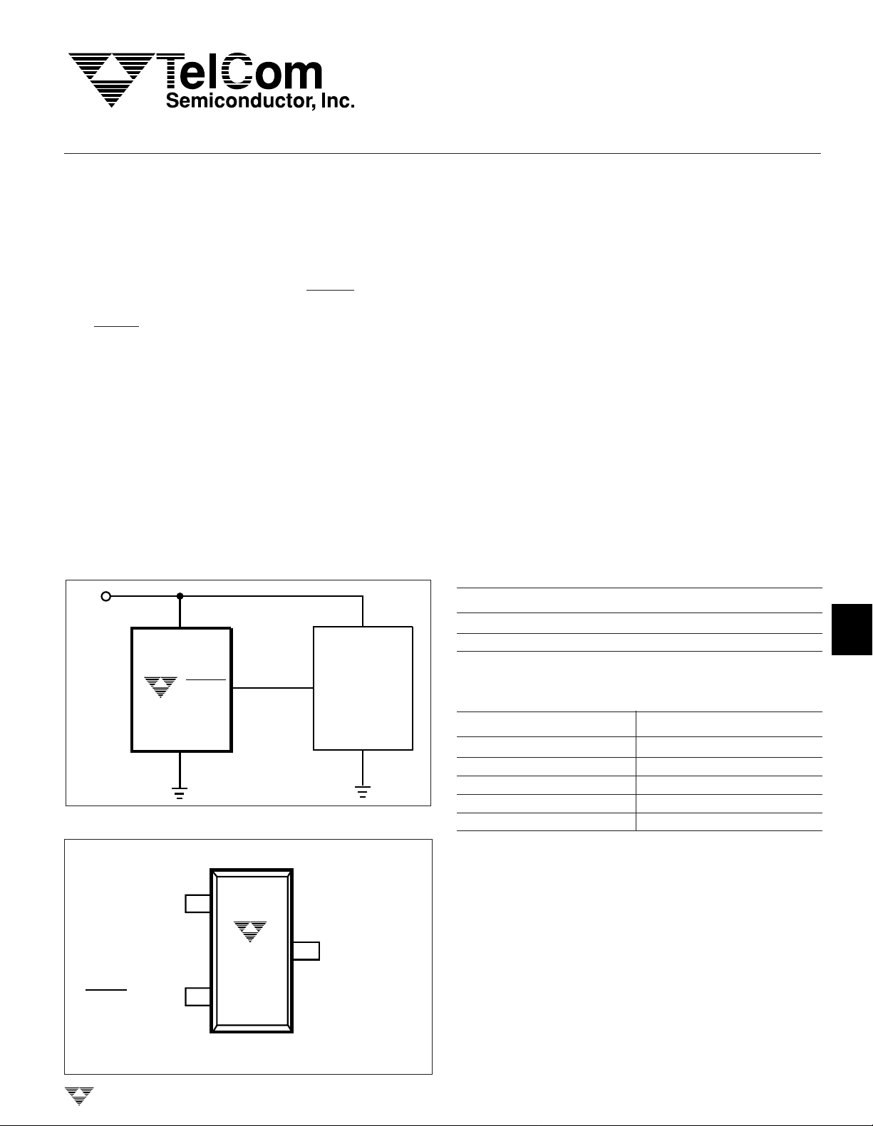
TYPICAL OPERATING CIRCUIT
V
CC
V
CC
V
CC
PROCESSOR
The TCM809 and TCM810 are cost-effective system
supervisor circuits designed to monitor VCC in digital systems and provide a reset signal to the host processor when
necessary. No external components are required.
The reset output is driven active within 20msec of V
falling through the reset voltage threshold. Reset is maintained active for a minimum of 140msec after VCC rises
above the reset threshold. The TCM810 has an active-high
reset output while the TCM809 has an active-low reset
output. The output of the TCM809 is guaranteed valid down
to VCC = 1V. Both devices are available in a
SOT-23B-3 package.
The TCM809/810 are optimized to reject fast transient
glitches on the VCC line. Low supply current of 17µA
(V
= 3.3V) makes these devices suitable for battery
CC
powered applications.
CC
ORDERING INFORMATION
Part No. Package Temp. Range
T
CM809xENB SOT-23B-3 – 40°C to +85 °C
TCM810xENB SOT-23B-3 – 40°C to +85 °C
NOTE: The "X" denotes a suffix for VCC threshold - see table below.
3
4
5
RESET
TCM809
GND
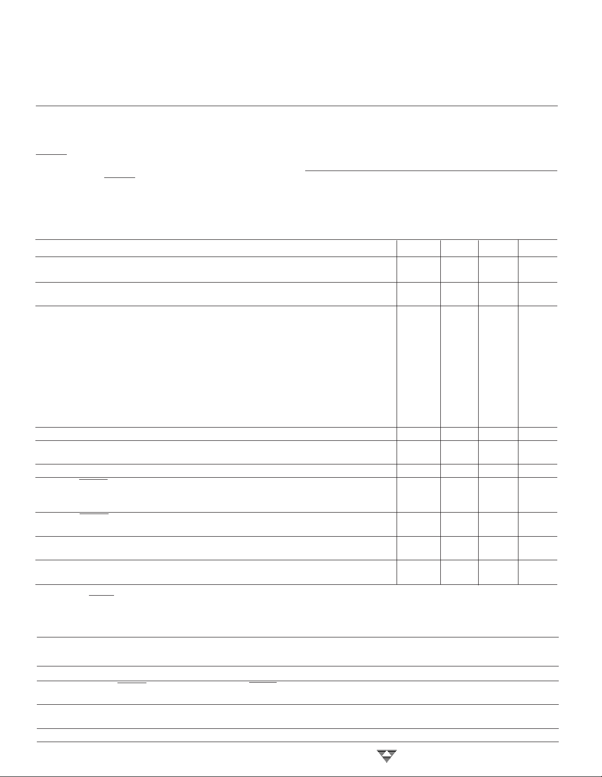
PIN CONFIGURATION
*SOT-23B-3
1
GND
TCM809xENB
TCM810xENB
RESET (RESET)
NOTE: *SOT-23B-3 is equivalent to JEDEC (TO-236)
** () is for TCM810
TELCOM SEMICONDUCTOR, INC.
2
3
RESET
INPUT
V
CC
GND
Suffix Reset VCC Threshold (V)
L
M 4.38
T 3.08
S 2.93
R 2.63
4.63
TCM809/810-04 8/29/96
5-15
6
7
8
Page 2
PRELIMINARY INFORMATION
TCM809
TCM810
3-PIN µP RESET MONITORS
ABSOLUTE MAXIMUM RATINGS*
Supply Voltage (V
RESET, RESET ............................ – 0.3V to (VCC + 0.3V)
Input Current, VCC....................................................20mA
Output Current, RESET, RESET .............................20mA
dV/dt (VCC) .......................................................... 100V/µS
Operating Temperature Range ...............– 40°C to +85°C
ELECTRICAL CHARACTERISTICS: V
to GND) ................................ +6.0V
CC
cc
= 5V, TA = Operating Temperature Range unless otherwise noted.
Power Dissipation (TA ≤ 70°C)
SOT-23B-3 (derate 4mW/°C above +70°C) ...230mW
Storage Temperature Range ................– 65°C to +150°C
Lead Temperature (Soldering, 10 sec) .................+260°C
*This is a stress rating only and functional operation of the device at these
or any other conditions above those indicated in the operational sections of
the specifications is not implied. Exposure to Absolute Maximum Rating
Conditions for extended periods may affect device reliability.
Symbol Parameter Test Conditions Min Typ Max Unit
VCC Range TA = 0°C to +70°C 1.0 — 5.5 V
TA = – 40°C to +85°C 1.2 — 5.5
I
CC
V
TH
V
OL
V
OH
V
OL
V
OH
NOTES: 1. Production testing done at TA = +25°C, over temperature limits guaranteed by design.
Supply Current TCM8xxL/M: VCC < 5.5V — 24 60 µA
TCM8xxR/S/T: VCC < 3.6V — 17 50
Reset Threshold (Note 2)
TCM8xxL: T
= – 40°C to +85°C 4.50 — 4.75
T
A
TCM8xxM: T
= – 40°C to +85°C 4.25 — 4.50
T
A
TCM8xxT: T
T
= – 40°C to +85°C 3.00 — 3.15
A
TCM8xxS: T
= – 40°C to +85°C 2.85 — 3.00
T
A
TCM8xxR: T
= +25°C 4.56 4.63 4.70 V
A
= +25°C 4.31 4.38 4.45
A
= +25°C 3.04 3.08 3.11
A
= +25°C 2.89 2.93 2.96
A
= +25°C 2.59 2.63 2.66
A
TA = – 40°C to +85°C 2.55 — 2.70
Reset Threshold Tempco — 30 — ppm/°C
VCC to Reset Delay (Note 2)
VCC = VTH to (VTH – 100mV) — 20 — µsec
Reset Active Timeout Period 140 240 560 msec
RESET Output Voltage Low TCM809R/S/T: VCC = VTH min, I
(TCM809) TCM809L/M: V
VCC > 1.0V, I
RESET Output Voltage High
(TCM809)
RESET Output Voltage Low
(TCM810)
TCM809R/S/T: VCC > VTH max, I
TCM809L/M: VCC > VTH max, I
T
CM810R/S/T: VCC = VTH max, I
T
CM810L/M: VCC = VTH max, I
RESET Output Voltage High 1.8 < VCC < VTH min, I
= VTH min, I
CC
SOURCE
SINK
= 1.2mA — — 0.3 V
SINK
= 3.2mA — — 0.4
SINK
= 50µA — — 0.3
= 500µA 0.8 V
SOURCE
= 800µAVCC – 1.5 — —
SOURCE
= 1.2mA — — 0.3 V
SINK
= 3.2mA — — 0.4
SINK
= 150µA 0.8 V
CC
CC
——V
——V
(TCM810)
2. RESET output for TCM809, RESET Output for TCM810.
PIN DESCRIPTION
Pin No.
(SOT-23B-3) Symbol Description
1 GND Ground
2 RESET (TCM809) RESET output remains low while V
for 240msec (140msec min.) after VCC rises above reset threshold.
2 RESET (TCM810) RESET output remains high while VCC is below the reset voltage threshold,
and for 240msec (140msec min.) after VCC rises above reset threshold.
3VCCSupply voltage (Typ. +3.0V to +5.0V)
5-16
is below the reset voltage threshold, and
CC
TELCOM SEMICONDUCTOR, INC.
Page 3

3-PIN µP RESET MONITORS
TCM809
V
CC
RESET
GND
RESET
GND
BUFFERED RESET
TO OTHER SYSTEM
COMPONENTS
BUFFER
µP
4.7k
V
CC
V
CC
PRELIMINARY INFORMATION
1
TCM809
TCM810
APPLICATIONS INFORMATION
V
Transient Rejection
CC
The TCM809/810 provides accurate V
and reset timing during power-up, power-down, and brownout/sag conditions, and rejects negative-going transients
(glitches) on the power supply line. Figure 1 shows the
maximum transient duration vs. maximum negative excursion (overdrive) for glitch rejection. Any combination of
duration and overdrive which lies under the curve will not
generate a reset signal. Combinations above the curve are
detected as a brownout or power-down. Transient immunity
can be improved by adding a capacitor in close proximity to
the VCC pin of the TCM809/810.
V
CC
Duration
V
TH
Overdrive
monitoring
CC
valid to VCC = 0V, a pull-down resistor must be connected
from RESET to ground to discharge stray capacitances and
hold the output low (Figure 2). This resistor value, though
not critical, should be chosen such that it does not appreciably load RESET under normal operation (100kΩ will be
suitable for most applications). Similarly, a pull-up resistor to
VCC is required for the TCM810 to ensure a valid high
RESET for VCC below 1.0V.
V
CC
V
CC
TCM809
RESET
R1
GND
Figure 2. Ensuring RESET Valid to VCC = 0V
100k
2
3
4
400
TA = +25°C
320
240
160
TCM8xxLM
80
TCM8xxR/S/T
0
MAXIMUM TRANSIENT DURATION (µsec)
1
RESET COMPARATOR OVERDRIVE,
Figure 1. Maximum Transient Duration vs.
Overdrive for Glitch Rejection at 25°C
RESET Signal Integrity During Power-Down
The TCM809 RESET output is valid to VCC = 1.0V.
Below this voltage the output becomes an "open circuit" and
does not sink current. This means CMOS logic inputs to the
µP will be floating at an undetermined voltage. Most digital
systems are completely shutdown well above this voltage.
However, in situations where RESET must be maintained
TELCOM SEMICONDUCTOR, INC.
10
(VTH - VCC (mV)
100
1000
Processors With Bidirectional I/O Pins
Some µP's (such as Motorola 68HC11) have bidirectional reset pins. Depending on the current drive capability
of the processor pin, an indeterminate logic level may result
if there is a logic conflict. This can be avoided by adding a
4.7k resistor in series with the output of the TCM809/810
(Figure 3). If there are other components in the system
which require a reset signal, they should be buffered so as
not to load the reset line. If the other components are
required to follow the reset I/O of the µP, the buffer should
be connected as shown with the solid line.
Figure 3. Interfacing to Bidirectional Reset I/O
5-17
5
6
7
8
Page 4

PRELIMINARY INFORMATION
TCM809
TCM810
TYPICAL CHARACTERISTICS
3-PIN
µP RESET MONITORS
SUPPLY CURRENT (µA)
Supply Current vs.Temperature
(No Load, TCM8xxR/S/T)
35
30
25
20
15
10
5
0
–40
–20 40 60
0
20
TEMPERATURE (°C)
Power-Down Reset Delay vs. Temperature
(TCM8xxR/S/T)
100
80
60
40
VCC = 5V
VCC = 3V
VCC = 1V
VOD = VTH – V
VOD = 10mV
VOD = 20mV
CC
85
SUPPLY CURRENT (µA)
Supply Current vs.Temperature
(No Load, TCM8xxL/M)
30
25
20
15
10
5
0
–40
–20 40 60
0
20
TEMPERATURE (°C)
Power-Down Reset Delay vs. Temperature
(TCM8xxL/M)
140
120
100
80
60
VCC = 5V
VCC = 3V
VCC = 1V
VOD = VTH – V
VOD = 10mV
VOD = 20mV
85
CC
20
POWER-DOWN RESET DELAY (µsec)
0
–40
–20 40 60
0
TEMPERATURE (°C)
Power-Up Reset Timeout vs. Temperature
250
245
240
235
230
POWER-UP RESET TIMEOUT (msec)
225
0
TEMPERATURE (°C)
5-18
–40
–20 40 60
20
20
VOD = 100mV
VOD = 200mV
TCM8xxL/M
TCM8xxR/S/T
85
85
40
20
POWER-DOWN RESET DELAY (µsec)
0
–40
–20 40 60
Normalized Reset Threshold vs. Temperature
1.003
1.002
1.001
1.000
0.999
0.998
NORMALIZED THRESHOLD
0.997
–40
–20 40 60
TELCOM SEMICONDUCTOR, INC.
0
0
20
TEMPERATURE (°C)
20
TEMPERATURE (°C)
VOD = 100mV
VOD = 200mV
85
85
 Loading...