

Page 1
Window Discriminator
TCA 965 B
Preliminary Bipolar IC
Features
● Two window settings
– direct setting of lower and upper edge
voltage (window edges)
– indirect setting by window center
voltage and half window width
● Adjustable hysteresis
● Digital outputs with open collectors
for currents up to 50 mA
● Adjustable reference voltage V
Stab
P-DIP-14-1
Type Ordering Code Package
■ TCA 965 B Q67000-A8338 P-DIP-14-1
■ Not for new design
The window discriminator compares an input voltage to a defined voltage window. The
digital outputs show whether the input voltage is below, within or above this window.
The TCA 965 B window discriminator is especially suitable as a tracking or
compensating controller with a dead band in control engineering and for the selection of
DC voltages within a certain tolerance of the required setpoint value in measurement
engineering. When it is used as a Schmitt trigger, switching frequencies up to a typical
value of 50 kHz are possible.
Semiconductor Group 1 1998-02-10
Page 2
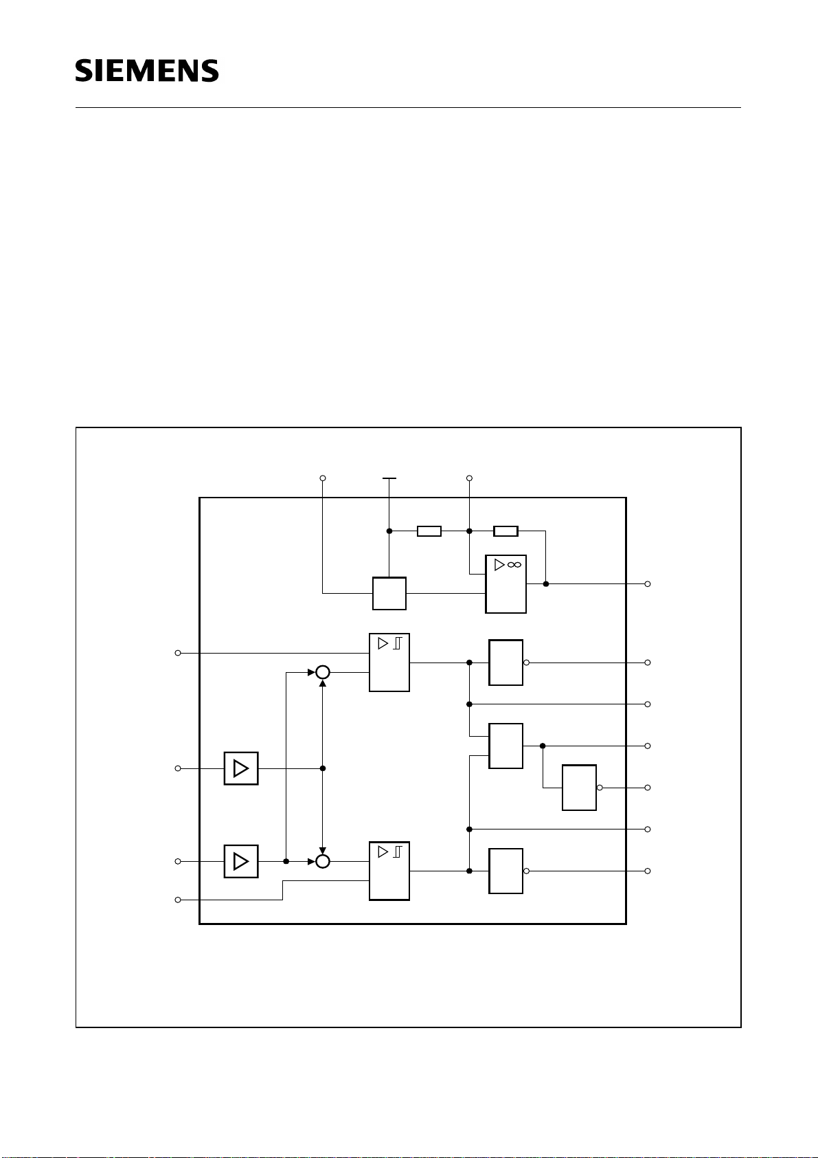
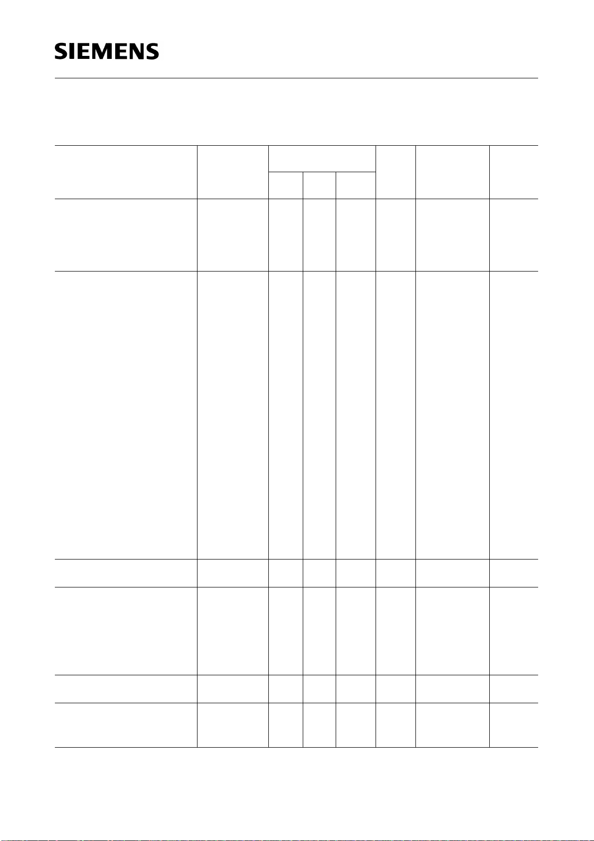
Functional Description
TCA 965 B
Amplifier Amp 3 increases the voltage of the reference source
R to V
= 2 x V
Stab
REF
. The
amplification factor can be altered by external wiring. With direct setting of the window,
the input voltage appears on amplifier Amp 1 (
comparator K2 (
V
) and the lower edge voltage on comparator K1 (V7).
6
With indirect setting of the window, the input voltage appears on inputs
the center voltage is connected to amplifier A1 (
V
The voltage applied to the input (
) of amplifier Amp 2 is subtracted symmetrically from
9
V
V
), the upper edge voltage on
8
V
and V7, while
6
).
8
the output voltage of amplifier Amp 1 and added. The comparators switch with
hysteresis. The logic gates have open-collector outputs.
If the inhibit input A or B is connected to ground, output A or B will always be high.
+
VV
S
11 1 5
R
REF
20 kΩ20 kΩ
_
Amp 3
+
10
V
Stab
V
V
V
V
7
7
Amp 1
8
8
V = 1
Amp 2
9
9
V = 1
6
6
_
+
+
_
Outputs A, B, C, D are open-collector
+
K1
_
+
K2
_
1
_
<
1
1
1
2
4
13
3
12
14
IEB00091
A
Inhibit A
C
D
Inhibit B
B
Block Diagram
Semiconductor Group 2 1998-02-10
Page 3
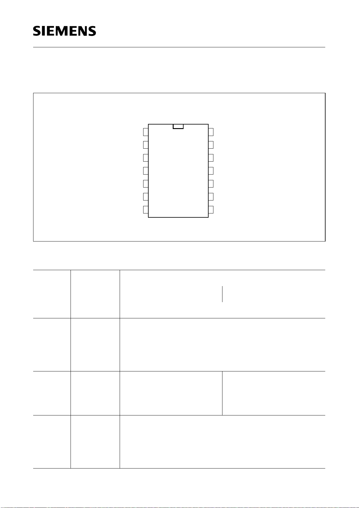
Pin Configuration
(top view)
TCA 965 B
TCA 965 B
GND
A
D
Inhibit A
V
REF
V
V
1
2
3
4
5
6
6
7
7
14
13
12
11
10
9
8
IEP00292
B
C
Inhibit B
V
+
S
V
Stab
V
9
V
8
Pin Definitions and Functions
Pin Symbol Pin Function in
Direct Setting Indirect Setting
of Window
1
2
3
4
5
6
7
8
9
10
11
12
13
14
GND
A
D
Inhibit A
V
REF
V
6
V
7
V
8
V
9
V
Stab
+ V
S
Inhibit B
C
B
GND
Logic output A
Logic output D = A @ B (AND)
Connected to GND: logic output A = HIGH
Internal
Upper edge voltage
Lower edge voltage
Input voltage
GND
Internal
V
V
REF
Stab
= 3 V
Input voltage
Input voltage V
Center voltage
Half window width
= 6 V
Supply voltage
Connected to GND: logic output B = HIGH
Logic output C = A @ B (NAND)
Logic output B
V
6/7
6/7
Semiconductor Group 3 1998-02-10
Page 4
TCA 965 B
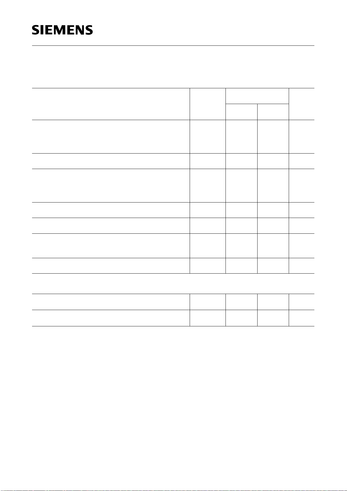
Absolute Maximum Ratings
Maximum ratings for ambient temperature
Parameter Symbol Limit Values Unit
T
= – 25 to 85 °C
A
min. max.
Supply voltage (pin 11)
Difference in input voltage between pins 6, 7, 8
Input voltage (pins 6, 7, 8, 9)
Output current (pins 2, 3, 13, 14)
Output voltage (pins 2, 3, 13, 14)
independent of
Voltage on V
V
REF
S
(pin 5)
Output current of stabilized voltage (pin 10)
Inhibit input voltage (pins 4, 12)
Junction temperature
Storage temperature
Thermal resistance system - air P-DIP-14-1
Operating Range
V
V
V
I
V
V
I
V
T
T
R
S
I
I
Q
Q
R
10
IH
j
stg
th SA
–
–
–
30
15
30
V
V
V
–50mA
–
–
–
30
8
V
V
–10mA
–7V
–55
150
125
°C
°C
– 80 K/W
Supply voltage
Ambient temperature
V
T
S
A
4.5 30 V
–25 85 °C
Semiconductor Group 4 1998-02-10
Page 5
Characteristics
V
= 10 V; TA= 25 °C
S
TCA 965 B
Parameter Symbol Limit Values Unit Test
Condition
min. typ. max.
Current consumption
I
S
–
5
7
mA
V
,
V
2
Input current
(pins 6, 7, 8)
Input current, pin 9
I
I
–I
–
I
–
20
400
50
3000
nA
nA
Input offset voltage in
direct setting of window
V
IO
–20
20
mV
Input offset voltage in
indirect setting of window
V
IO
–50
50
mV
Input-voltage range on
pins 6, 7, 8
V
I
1.5
V
S
–1
V
∆
V
I
Input-voltage range on
pin 9
Differential input voltage
V
V
(
V
I
–(
6
8
50
V
–
V
)
8
9
+
V
)–
V
9
7
V
13
13
S
/2
mV
V
V
=
V
13
QH
<13V
Test
Circuit
1
1
1
1
2
1
2
Reference voltage
Stabilized voltage on
pin 10
TC of reference voltage
Sensitivity of reference
voltage to supply-voltage
variation
Output reverse current
Output saturation voltage
Hysteresis of window
edges
Inhibit threshold
Inhibit current
Switching frequency
V
5
V
10
αV
5
∆V5/∆V
I
QH
V
QL
V
– V
U
V
4, 12
I
4, 12
f
dir
f
ind
2.8
5.536
3.2
6.5
0.4
S
2
V
V
mV/K
mV/V
I
= 0
REF
V
> 7.9 V
S
––10µA– –
100
500
L
18
22
1
–
–
– 100
2050–
–
200
800
35
1.8
– µA– –
–
mV
mV
mV
V
kHz
kHz––
I
= 10 mA
Q
I
= 50 mA
Q
1
1
2
Semiconductor Group 5 1998-02-10
Page 6
TCA 965 B
V
S
Ι
S11
11
6
Ι
62
3
13
Ι
Ι
7
7
TCA 965B
14
10
Ι
8
Ι
8
5
RLRLRLR
ΙΙ
QH2
Ι
QH3
Ι
QH13
Ι
QH14
L
= ==
V
V
6
V
7
914 12
8
Ι
Ι
Test Circuit 1
Direct Setting of Window
V
9
V V
= =
4
5
12
V
10
V
QL14
V
QL13
V
QL3
V
QL2
IES00086
Semiconductor Group 6 1998-02-10
Page 7

TCA 965 B
V
S
Ι
S11
11
6
2
3
RLRLRLR
Ι
QH2
Ι
QH3
L
7
TCA 965B
13
14
Ι
QH13
Ι
QH14
8
10
9
= ==
V
6/7
V
V
8
9
14 12
V V
= =
4
5
12
V
5
V
10
V
QL14
V
QL13
Test Circuit 2
Indirect Setting of Window by Center Voltage and Half Window Width
V
QL3
V
QL2
IES00087
Semiconductor Group 7 1998-02-10
Page 8

TCA 965 B
Inhibit Inputs 4,12
V
S
100 1 k
V
4,12
ΩΩ
V
4,12
GND High
Outputs A, B
V
6,7,8
Inputs 6, 7, 8
1 k
Ω
Outputs 2, 3, 13, 14
Input 9
Outputs
V
9
V
,
REFVStab
Not permitted> 7 V
Normal functionopen
Low> 1.8 V
V
Stab
R
V
REF
Q
IES00088
Schematic Circuit Diagrams
Semiconductor Group 8 1998-02-10
Page 9

TCA 965 B
V
S
C
1
R
1
10 11
R
4
R
2
6
V
6
2
3
A
D
TCA 965 B
7
R
5
C
2
R
V
Ι
R
6
C
3
7
R
3
V
7
8
V
8
V
9
1
9
412
13
14
C
B
IES00294
To increase the switching frequency, pin 9 may be grounded
R
V
via
approx. 30...40 mV).
7(9
Application Circuit 1
Direct Setting of Lower and Upper Edge Voltages
V
– V9 = Upper edge voltage
6
V
+ V9 = Lower edge voltage
7
V
= Input voltage
8
Semiconductor Group 9 1998-02-10
Page 10

TCA 965 B
V
10
A
V
L
V
U
t
Definition of the Offset Voltage V
V
V
+
L
V
10
---------------------
U
V
–=
2
7
IO
V
7
IES00296
Semiconductor Group 10 1998-02-10
Page 11

TCA 965 B
V
8
Pin 4 on GND
A
B
Upper
Edge
Lower
Edge
V
6
V
7
t
LU
A
B
C
D
Inhibit A
1
0
t
1.8 V < Pin 4 < 7 V
A
B
t
1
0
C
C
D
D
Inhibit B
Pin 12 on GND
A
B
C
DD
tt
t
UL
1
0
1.8 V < Pin 12 < 7 V
A
B
C
LU
t
1
0
1
0
1
0
1
0
1
0
IES00295
Application Circuit 1
Direct Setting of Lower and Upper Edge Voltages
Semiconductor Group 11 1998-02-10
Page 12

RR
1
3
10 11
TCA 965 B
V
S
C
1
C
2
R
5
R
6
8
V
8
9
V
9
2
3
A
D
TCA 965 B
R
V
Ι
7
C
3
RR
4
2
6
V
6
7
V
7
1
412
13
14
C
B
IES00297
Application Circuit 2
Indirect Setting of Window by Center Voltage and Half-Window Width V
V
= V7 = Input voltage
6
V
= Center voltage
8
V
= Half window width
9
Semiconductor Group 12 1998-02-10
Page 13

TCA 965 B
V
10
B
V
=
10
Definition of the Offset Voltage V
V
V
+
L
V
10
---------------------
U
2
V8V
)–(–=
9
V
L
V
-
L
2
IO
V
U
V
V
-
8
V
U
V
V
()
-
-
8
9
t
9
IES00299
Semiconductor Group 13 1998-02-10
Page 14

TCA 965 B
V
8
Upper
Edge
Lower
Edge
V
6
V
7
t
LU
t
A
B
C
D
Inhibit A
Pin 4 on GND 1.8 V < Pin 4 < 7 V
A
B
C
D
1
A
0
B
C
D
t
1
0
1
0
1
0
Inhibit B
Pin 12 on GND 1.8 V < Pin 12 < 7 V
A
B
C
D
tt
t
UL
A
1
B
0
C
D
LU
t
1
0
1
0
1
0
IED00298
Application Circuit 2
Indirect Setting of Window by Center Voltage and Half-Window Width V
Semiconductor Group 14 1998-02-10
Page 15

TCA 965 B
V
S
R
R
R
10 11
R
1
13
L
L
L
6
V
Ι
8
14
2
TCA 965B
V
6
R
4
PR
V
H
=
5
IES00089
R
2
7
R
3
V
3
V
H
0
V
7
1
3
9
V
8
Application Circuit 3
Symmetrically Enlarged Edge Hysteresis in Direct Setting of Window
Calculation of Hysteresis
R
=
V
H
V
10
-------------------
R4R
+
V
5
10
5
-------------------
R4R
+
5
V
--------------------------------
R1R2R
10
++
3
V
H
10 mA≤+
Semiconductor Group 15 1998-02-10
Page 16

TCA 965 B
V
S
R
R
10 11
R
R
1
2
L
L
L
8
V
Ι
R
2
V
3
0
6
7
V
9/2
TCA 965B
1
V
9/1
14
13
3
9/1
5
R
3
R
4
V
6/7
IES00090
R
9
=
V
H
VV
-
9/2
V
8
Application Circuit 4
Symmetrically Enlarged Edge Hysteresis in Indirect Setting of Window
Calculation of Hysteresis
V
V
V
= V
H
9/1
9/2
– V
9/2
=
=
9/1
R4R
V
-------------------------------
10
R3R4R
+
R
V
-------------------
10
R3R
+
||
5
||
4
4
V
H
5
Semiconductor Group 16 1998-02-10
Page 17

P-DIP-14-1
(Plastic Dual In-line Package)
TCA 965 B
GPD05005
Sorts of Packing
Package outlines for tubes, trays etc. are contained in our
Data Book “Package Information”.
Dimensions in mm
Semiconductor Group 17 1998-02-10
 Loading...