

Page 1
2-Phase Stepper-Motor Driver
TCA 3727
Overview Bipolar IC
Features
• 2 x 0.75 amp. / 50 V outputs
• Integrated driver, control logic and current control
(chopper)
• Fast free-wheeling diodes
• Max. supply voltage 52 V
• Outputs free of crossover current
• Offset-phase turn-ON of output stages
• Z-diode for logic supply
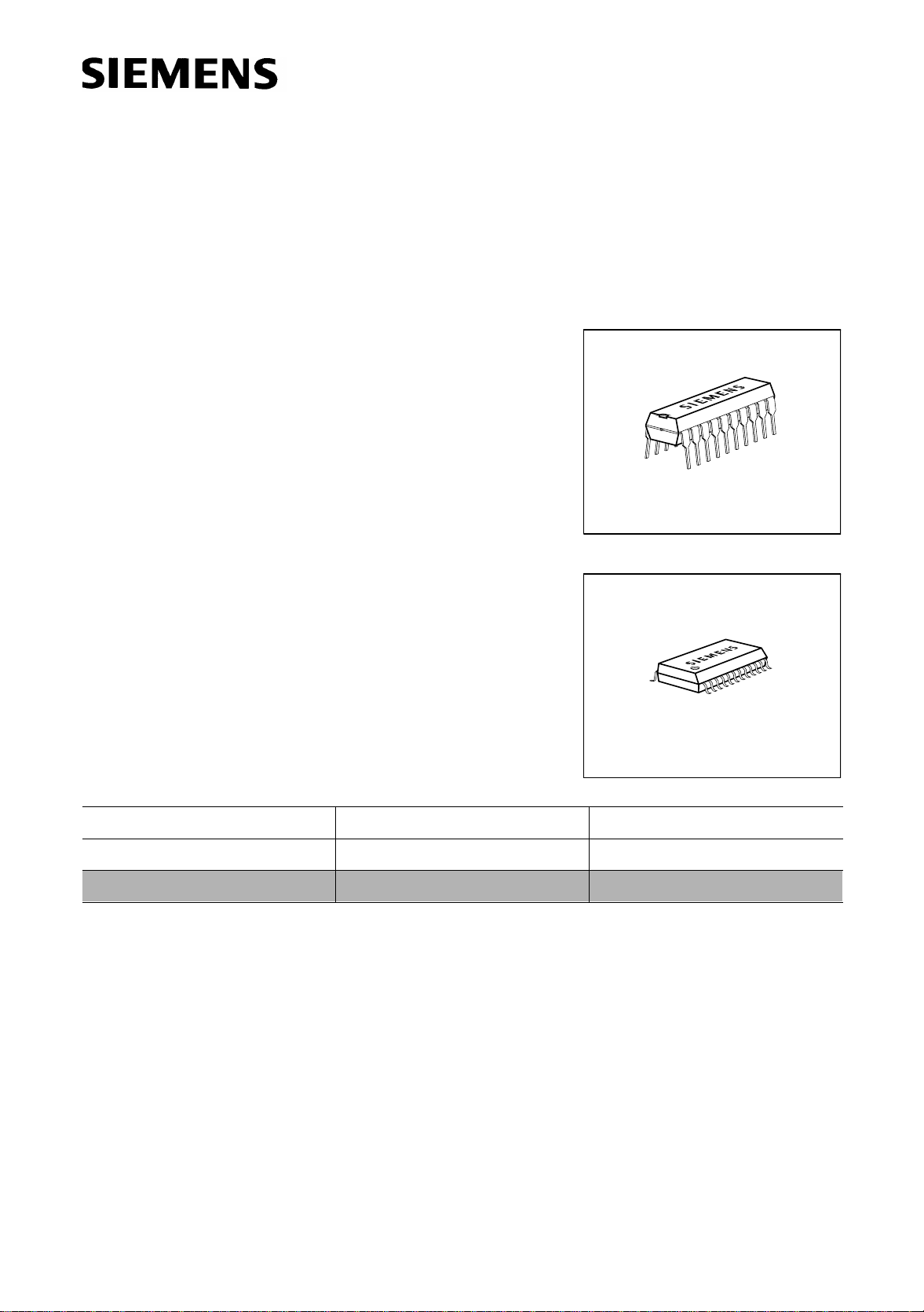
P-DIP-20-6
• Low standby-current drain
• Full, half, quarter, mini step
P-DSO-24-3
Type Ordering Code Package
TCA 3727 Q67000-A8302 P-DIP-20-6
TCA 3727 G Q67000-A8335 P-DSO-24-3
Description
TCA 3727 is a bipolar, monoli thic IC for driving bipolar s tepper motors, DC motors and
other inductive loads that operate on constant current. The control logic and power
output stages for two bipolar windings are integrated on a single chip which permits
switched current control of motors with 0.75 A per phase at operating voltages up to
50 V.
Semiconductor Group 1 1998-02-01
Page 2

TCA 3727
The direction and value of current are programmed for each phase via separate control
inputs. A common oscillator generates the timing for the current control and turn-on with
phase offset of the two output stages. The two output stages in a full-bridge configuration
have integrated, fast free-wheeling diodes and are free of crossover current. The logic is
supplied either sep arately with 5 V or taken f rom the motor su pply voltage b y way of a
series resistor and an integrated Z-diode. The device can be driven directly by a
microprocessor with the possibility of a ll modes from ful l step through ha lf step to mini
step.
Semiconductor Group 2 1998-02-01
Page 3
TCA 3727 TCA 3727 G
TCA 3727
1
10
Ι
2
11
Ι
Phase 1
OSC
GND
GND
3
4
5
6
7
8
12
V
9
S
Q12
10
20
19
18
17
16
15
14
13
12
11
IEP00696
Ι
20
21
Ι
Phase 2
Inhibit
GND
GND
Q21Q11
RR
V
L
Q22
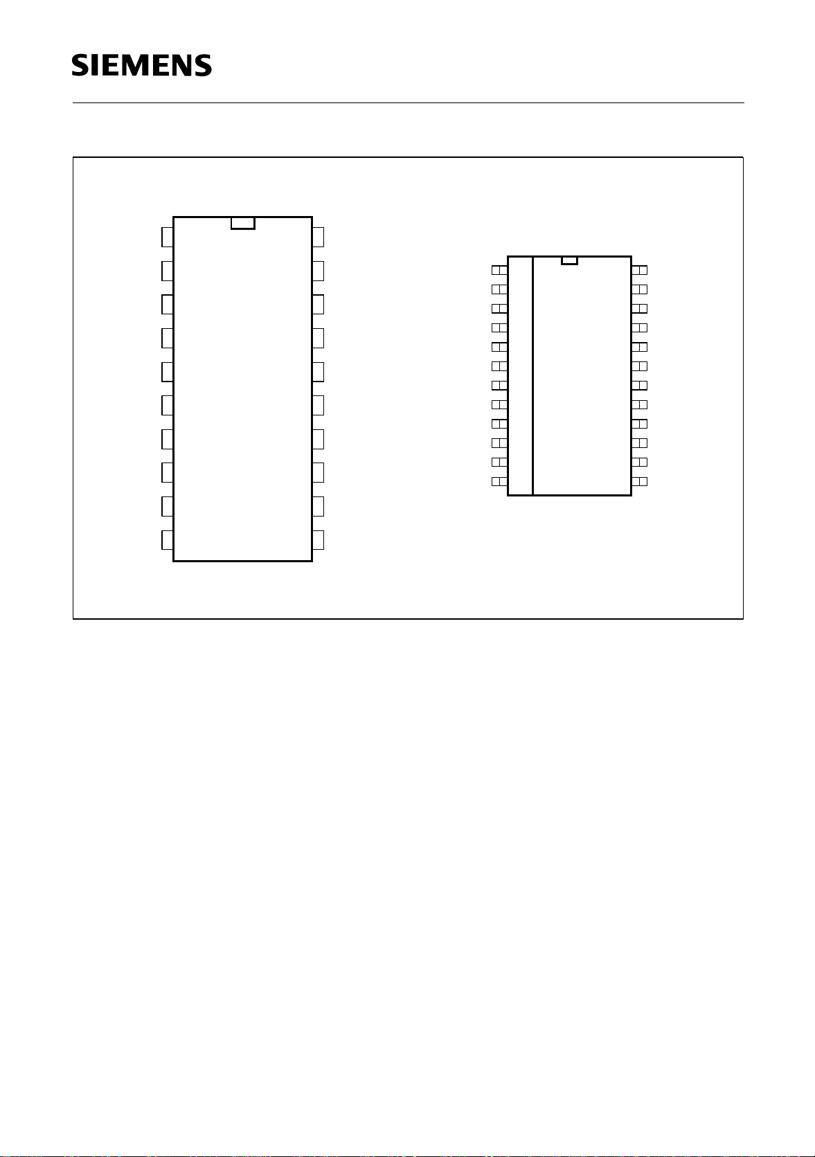
Figure 1 Pin Configuration (top view)
10
Ι
Ι
11
Phase 1
OSC
GND
GND
GND
GND
Q11
R
1
++
V
S
Q12
241
232
223
214
205
196
187
178
169
1510
1411
1312
IEP00898
21
Ι
Phase 2
Inhibit
GND
GND
GND
GND
Q21
R
2
V
L
Q22
20
Ι
Semiconductor Group 3 1998-02-01
Page 4
Pin Definitions and Functions
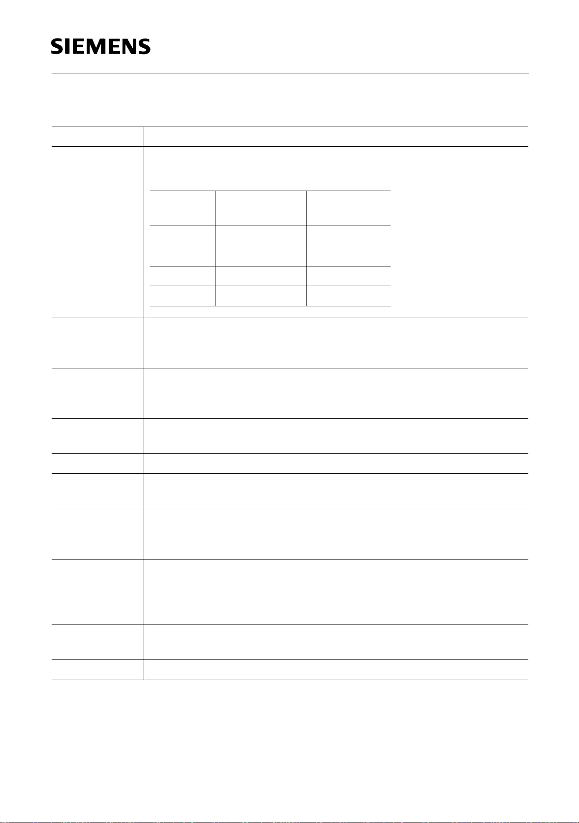
Pin No. Function
TCA 3727
1, 2, 19, 20
(1, 2, 23, 24)
Digital control inputs IX0, IX1 for the magnitude of the current of
1)
the particular phase.
IX1 IX0 Phase Current Example of
Motor Status
H H 0 No current
H L 1/3
LH 2/3
LL
I
max
I
I
max
max
Hold
Set
Accelerate
typical I
R
= 1 Ω : 750 mA
sense
max
with
3 Input Phase 1; controls the current through phase winding 1. On
H-potential the phase current flows from Q11 to Q12, on L-potential in
the reverse direction.
5, 6, 15, 16
Ground; all pins are connected internally.
(5, 6, 7, 8, 17,
18, 19, 20)
1)
4 Oscillator; works at approx. 25 kHz if this pin is wired to ground
across 2.2 nF.
8 (10)
1)
7, 10 (9, 12)
Resistor R1 for sensing the current in phase 1.
1)
Push-pull outputs Q11, Q12 for phase 1 with integrated
free-wheeling diodes.
9 (11)
1)
Supply voltage; block to ground, as close as possible to the IC, with
a stable electrolytic capacitor of at least 10 µF in parallel with a
ceramic capacitor of 220 nF.
12 (14)
1)
Logic supply voltage; either supply with 5 V or connect to + VS
across a series resistor. A Z-diode of approx. 7 V is integrated. In both
cases block to ground directly on the IC with a stable electr olytic
capacitor of 10 µF in parallel with a ceramic capacitor of 100 nF.
11, 14
(13, 16)
13 (15)
Semiconductor Group 4 1998-02-01
1)
1)
Push-pull outputs Q22, Q21 for phase 2 with integrated free
wheeling diodes.
Resistor R2 for sensing the current in phase 2.
Page 5

Pin Definitions and Functions (cont’d)
Pin No. Function
17 (21)
1)
Inhibit input; the IC can be put on standby by low potential on this
pin. This reduces the current consumption substantially.
18 (22)
1)
Input phase 2; controls the current flow through phase winding 2. On
H-potenti al the phase cur rent flows fr om Q21 to Q22, on L potential i n
the reverse direction.
1)
TCA 3727 G only
TCA 3727
Semiconductor Group 5 1998-02-01
Page 6
TCA 3727
+
V
LS
12 9
V
+
10
Ι
11Ι
Phase 1
Inhibit
20Ι
4
1
2
3
17
20
OSC
Function
Logic
Phase 1
Inhibit
10
14
7
8
Q11
Q12
R
1
Q21
Phase 1
Phase 2
Q22
21Ι
19
Function
Logic
11
Phase 2
Phase 2
18
13
R
2
5, 6, 15, 16
GND
IEB00697
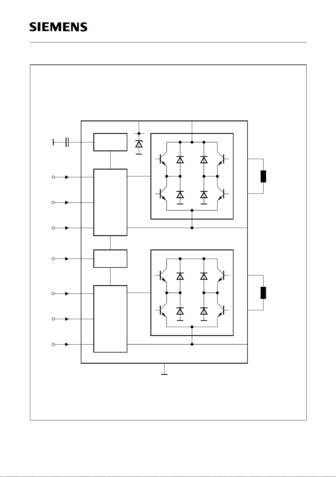
Figure 2 Block Diagram TCA 3727
Semiconductor Group 6 1998-02-01
Page 7
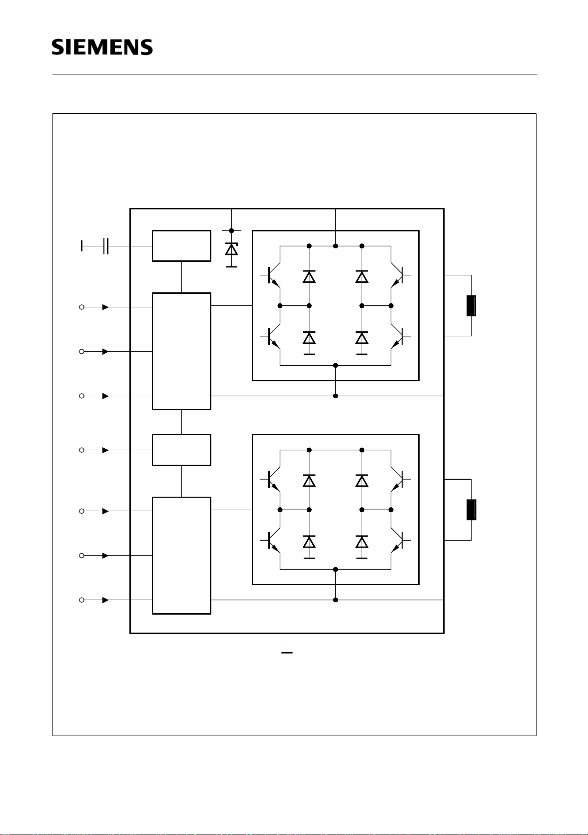
TCA 3727
Ι
10
11
Ι
Phase 1
Inhibit
4
1
2
3
21
Oscillator
Functional
Logic
Phase 1
Inhibit
V
+
LS
V
+
14 11
T11
T13
T21
D12D11
T12
D14D13
T14
D21 D22
T22
12
10
16
9
Q11
Q12
R
1
Q21
Phase 1
Ι20
Ι21
24
23
Functional
Logic
Phase 2
Phase 2
22
Figure 3 Block Diagram TCA 3727 G
T23
5-8, 17-19
GND
D23 D24
T24
13
15
IEB00899
Q22
R
2
Phase 2
Semiconductor Group 7 1998-02-01
Page 8
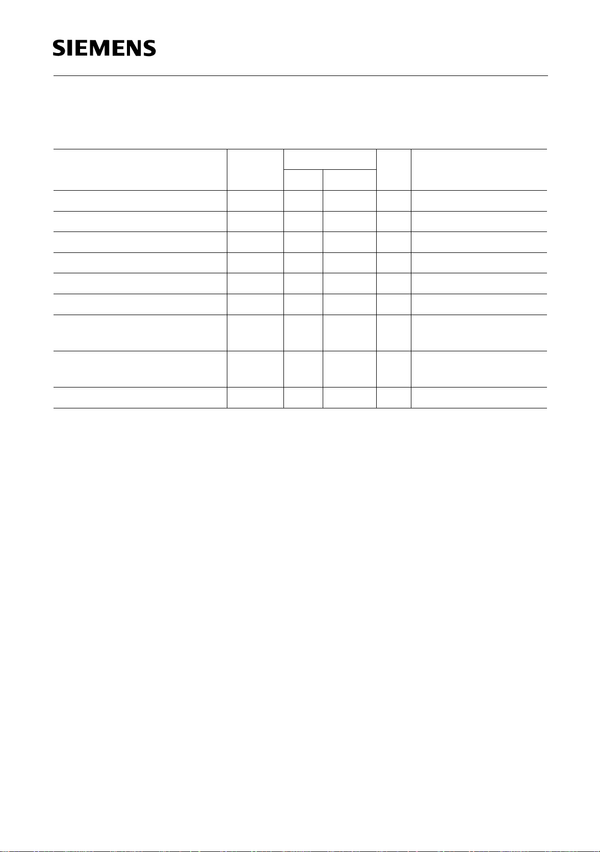
Absolute Maximum Ratings
T
= – 40 to 125 °C
A
Parameter Symbol Limit Values Unit Remarks
min. max.
TCA 3727
Supply voltage
Logic supply voltage
Z-current of
V
L
Output current
Ground current
Logic inputs
R
, R2, oscillator input voltage V
1
Junction temperature
Storage temperature
V
V
I
L
I
Q
I
GND
V
V
T
T
T
S
L
Ixx
RX,
OSC
j
j
stg
052 V–
0 6.5 V Z-diode
–50 mA–
– 1 1 A –
– 2 2 A –
– 6 VL + 0.3 V IXX; Phase 1, 2; Inhibit
– 0.3 VL + 0.3 V –
–
–
125
150
°C°C–
max. 1,000 h
– 50 125 °C–
Semiconductor Group 8 1998-02-01
Page 9
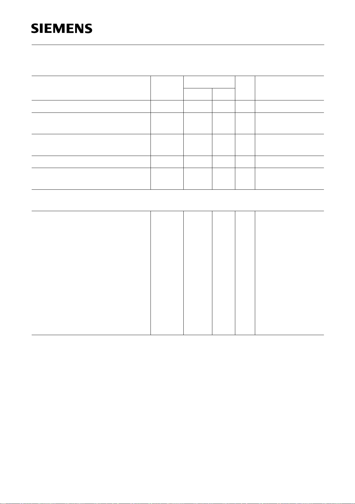
Operating Range
Parameter Symbol Limit Values Unit Remarks
min. max.
TCA 3727
Supply voltage
Logic supply voltage
Case temperature
Output current
Logic inputs
Thermal Resistances
Junction ambient
Junction ambient
(soldered on a 35 µm thick 20 cm
PC board copper area)
Junction case
V
V
S
L
550V–
4.5 6.5 V without series
resistor
T
I
V
C
Q
IXX
– 40 110 °C measured on pin 5
P
= 2 W
diss
– 1000 1000 mA –
– 5 V
V IXX; Phase 1, 2;
L
Inhibit
R
th ja
R
th ja
2
R
th jc
–
–
–
56
40
18
K/W
K/W
K/W
P-DIP-20-3
P-DIP-20-3
measured on pin 5
P-DIP-20-3
Junction ambient
Junction ambient
(soldered on a 35 µm thick 20 cm
PC board copper area)
Junction case
R
th ja
R
th ja
2
R
th jc
–
–
–
75
50
15
K/W
K/W
K/W
P-DSO-24-3
P-DSO-24-3
measured on pin 5
P-DSO-24-3
Semiconductor Group 9 1998-02-01
Page 10
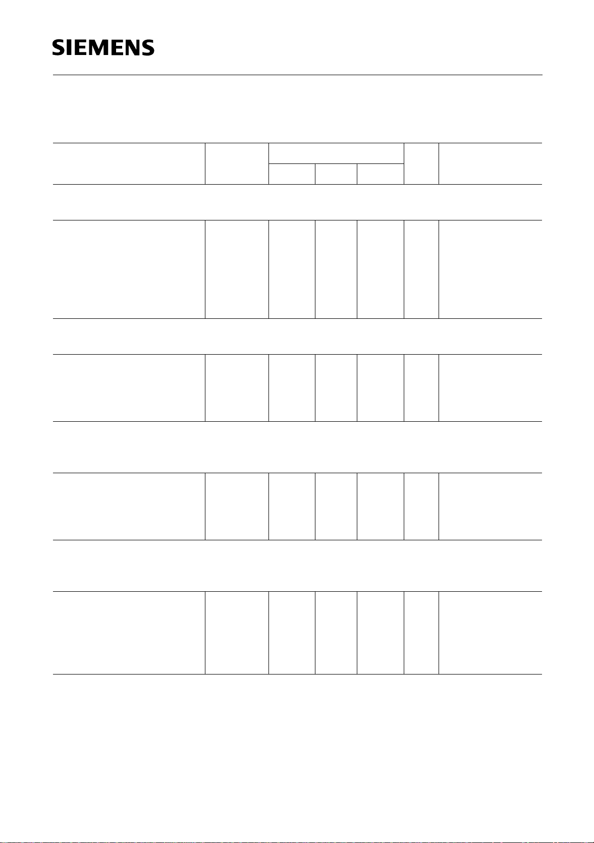
TCA 3727
Characteristics
V
= 40 V; VL = 5 V; – 25 °C ≤ Tj ≤ 125 °C
S
Parameter Symbol Limit Values Unit Test Condition
min. typ. max.
Current Consumption
from +
from + V
from + V
from + V
V
S
S
L
L
Oscillator
Output charging current
Charging threshold
Discharging threshold
Frequency
Phase Current Selection (
Current Limit Threshold
No current
Hold
Setpoint
Accelerate
I
S
I
S
I
L
I
L
I
OSC
V
OSCL
V
OSCH
f
OSC
R
1; R2
V
sense n
V
sense h
V
sense s
V
sense a
–
–
–
–
–
–
–
18
0.2
16
1.7
18
110
1.3
2.3
25
0.5
20
3
25
–
–
–
35
mA
mA
mA
mA
µA
V
V
kHz
V
V
I
Q1/2
V
V
I
Q1/2
–
–
–
C
inh
inh
inh
inh
OSC
= L
= H
= 0, I
= L
= H
= 0, I
= 2.2 nF
XX = L
XX = L
)
–
200
460
740
0
250
540
825
–
300
620
910
mV
mV
mV
mV
IX0 = H; IX1 = H
IX0 = L; IX1 = H
IX0 = H; IX1 = L
IX0 = L; IX1 = L
Logic Inputs
I
; IX0; Phase x)
(
X1
Threshold
L-input current
L-input current
H-input current
Semiconductor Group 10 1998-02-01
V
I
I
I
I
IL
IL
IH
1.4
(H→L)
– 10
– 100
–
–
2.3
V
–
(L→H)
V
–
–
–
–
–
10
µA
µA
µA
= 1.4 V
I
V
= 0 V
I
V
= 5 V
I
Page 11
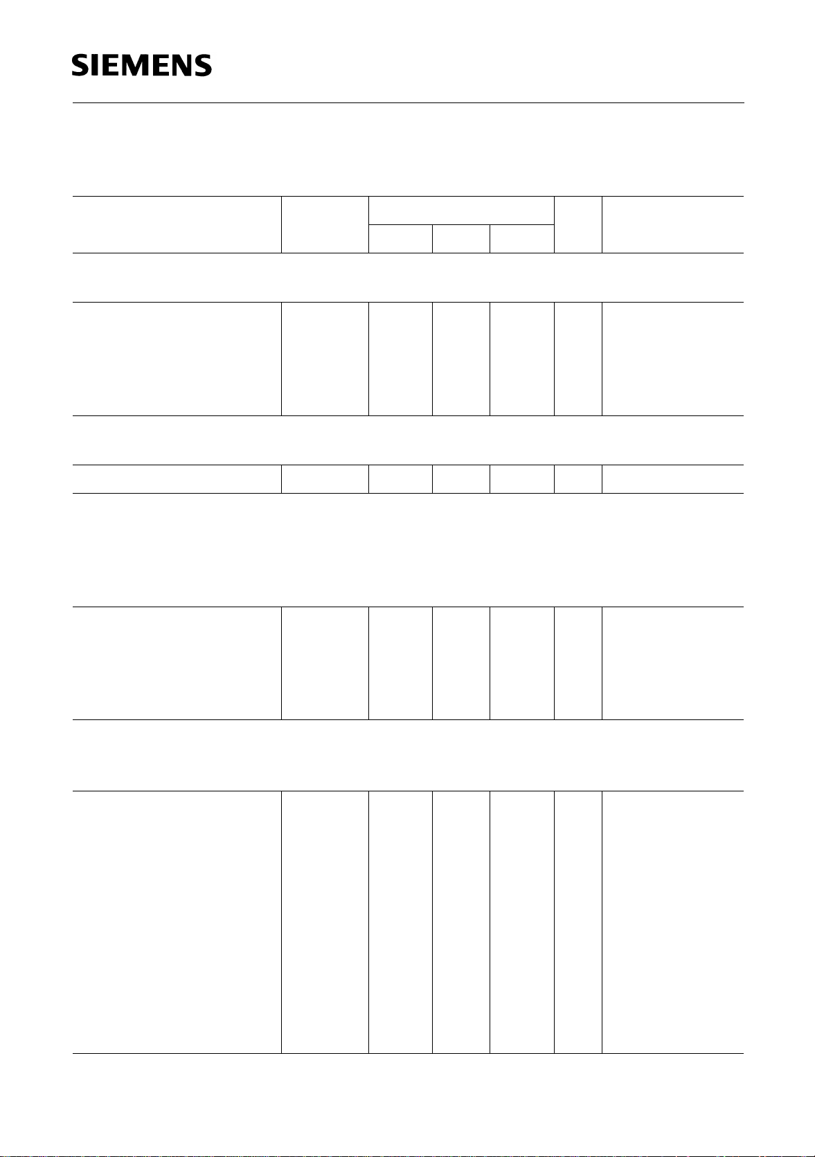
TCA 3727
Characteristics (cont’d)
V
= 40 V; VL = 5 V; – 25 °C ≤ Tj ≤ 125 °C
S
Parameter Symbol Limit Values Unit Test Condition
min. typ. max.
Standby Cutout (inhibit)
V
Threshold
Threshold
Hysteresis
Internal Z-Diode
Inh
(L→H)
V
Inh
(H→L)
V
Inhhy
2
1.7
0.3
3
2.3
0.7
4
2.9
1.1
V
V
V
–
–
–
Z-voltage
V
LZ
6.5 7.4 8.2 V IL = 50 mA
Power Outputs
Diode Transistor Sink Pair
(D13, T13; D14, T14; D23, T23; D24, T24)
Saturation voltage
Saturation voltage
Reverse current
Forward voltage
Forward voltage
V
V
I
V
V
satl
satl
Rl
Fl
Fl
–
–
–
–
–
Diode Transistor Source Pair
(D11, T11; D12, T12; D21, T21; D22, T22)
Saturation voltage
Saturation voltage
Saturation voltage
Saturation voltage
Reverse current
Forward voltage
Forward voltage
Diode leakage current
V
V
V
V
I
V
V
I
Ru
SL
satuC
satuD
satuC
satuD
Fu
Fu
–
–
–
–
–
–
–
–
0.3
0.5
–
0.9
1
0.9
0.3
1.1
0.5
–
1
1.1
1
0.6
1
300
1.3
1.4
1.2
0.7
1.4
1
300
1.3
1.4
2
V
V
µA
V
V
V
V
V
V
µA
V
V
mA
I
= – 0.5 A
Q
I
= – 0.75 A
Q
V
= 40 V
Q
I
= 0.5 A
Q
I
= 0.75 A
Q
I
= 0.5 A;
Q
charge
I
= 0.5 A;
Q
discharge
I
= 0.75 A;
Q
charge
I
= 0.75 A;
Q
discharge
V
= 0 V
Q
I
= – 0.5 A
Q
I
= – 0.75 A
Q
I
= – 0.75 A
F
Semiconductor Group 11 1998-02-01
Page 12
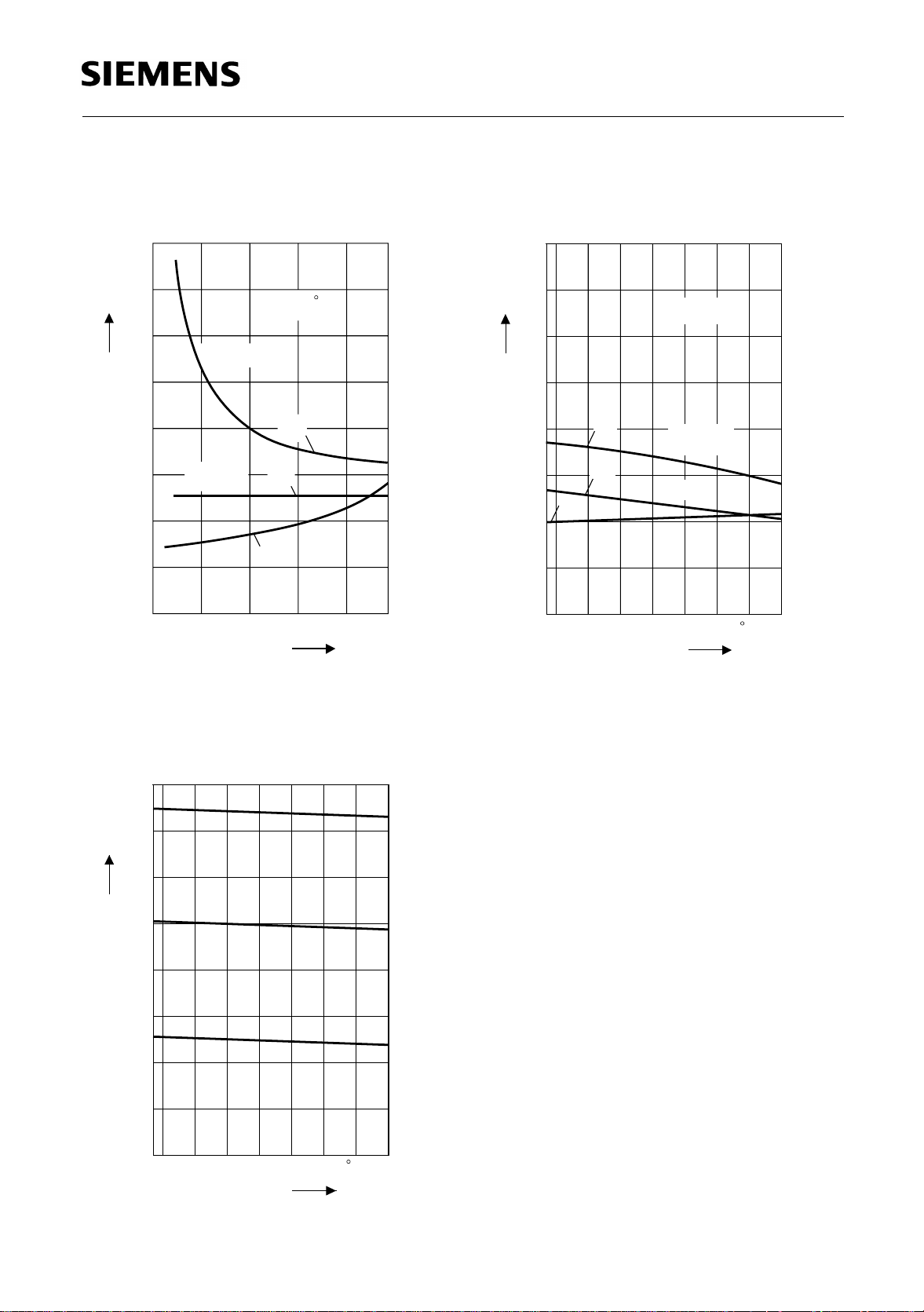
TCA 3727
Quiescent Current IS, IL versus
V
XX
= H
= L
S
T
Ι
= 25 C
j
Ι
L
Ι
L
S
IED01655
V
S
Supply Voltage
40
mA
Ι
Ι
S,L
30
Ι
20
Ι
XX
10
0
0102030V50
Quiescent Current
I
, IL versus
S
Junction Temperature
40
mA
ΙΙ
,
S
L
30
20
10
0
-25 0 25 50 75 100 150C
Ι
L
Ι
L
Ι
S
V
Ι
Ι
XX
T
j
= 40V
S
= L
XX
= H
IED01656
T
j
I
Output Current
versus
QX
Junction Temperature
800
mA
Ι
QX
600
400
200
0
-25 0 25 50 75 100 C 150
T
j
IED01657
T
j
Operating Condition:
V
L
V
Inh
C
R
sense
OSC
= 5 V
= H
= 2.2 nF
= 1 Ω
Load: L = 10 mH
R = 2.4 Ω
f
phase
mode: fullstep
= 50 Hz
Semiconductor Group 12 1998-02-01
Page 13
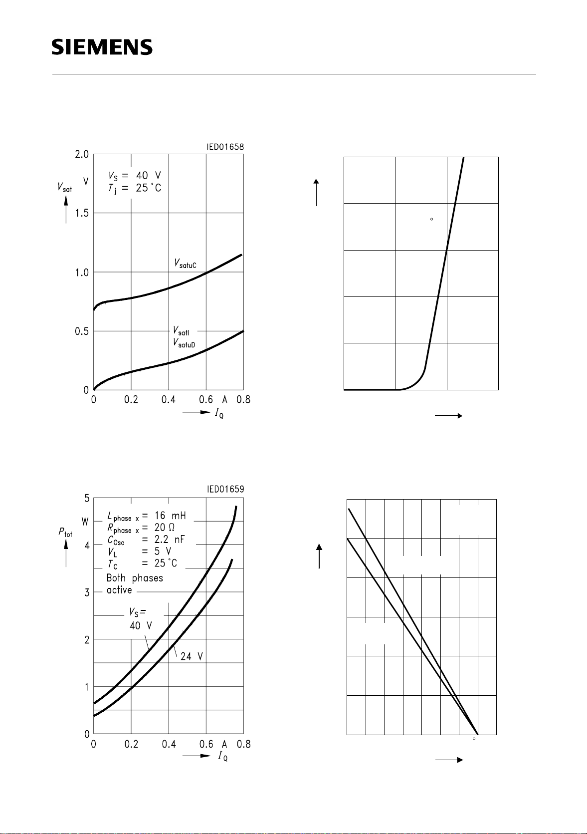
TCA 3727
Output Saturation Voltages V
versus Output Current IQ
sat
Forward Current
I
of Free-Wheeling
F
Diodes versus Forward Voltages
Fl
1.0
IED01167
Fu
V
V
F
1.0
Ι
F
A
0.8
0.6
0.4
0.2
0
0
0.5
VV
T
= 25 C
j
V
1.5
F
Typical Power Dissipation
I
Output Current
(Non Stepping)
Q
P
tot
versus
Permissible Power Dissipation
P
versus Case Temperature TC
12
W
P
tot
10
P-DSO-24
8
6
P-DIP-20
4
2
0
100-25 0 5025 75 C
IED01660
Measured
at pin 5.
125
T
c
175
tot
Semiconductor Group 13 1998-02-01
Page 14
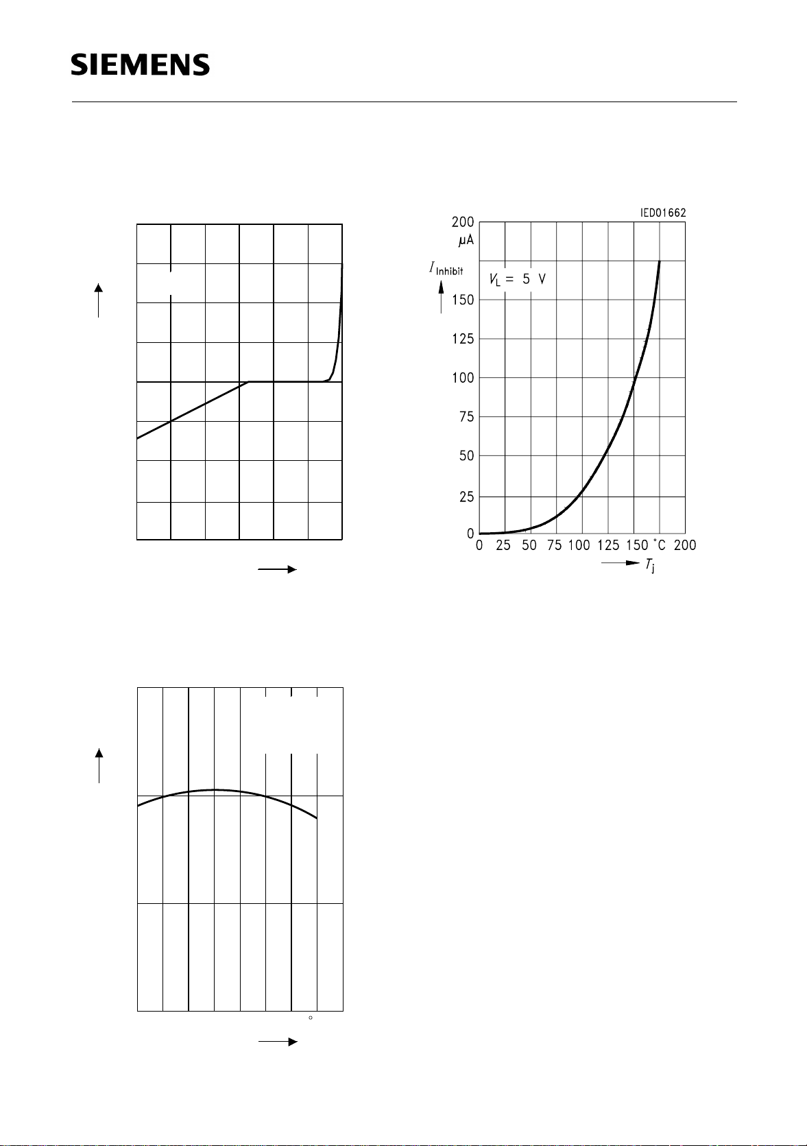
TCA 3727
Input Characteristics of Ixx, Phase X,
Inhibit
IED01661
V
V
IXX
Ι
0.8
mA
0.6
IXX
V
= 5V
L
0.4
0.2
0
0.2
0.4
0.6
0.8
-6 -5 -2 3.9 2 6
Input Current of Inhibit versus
JunctionTemperature
T
j
Oscillator Frequency
Junction Temperature
30
V
V
C
f
kHz
OSC
25
20
15
-25 0 25 50 75 100 125 C 150
f
OSC
T
S
L
OSZ
versus
j
IED01663
= 40V
= 5V
= 2.2nF
T
j
Semiconductor Group 14 1998-02-01
Page 15
TCA 3727
µ
Ι
ΙL
Ι
H
Ι
V
L
Ι
V
H
Ι
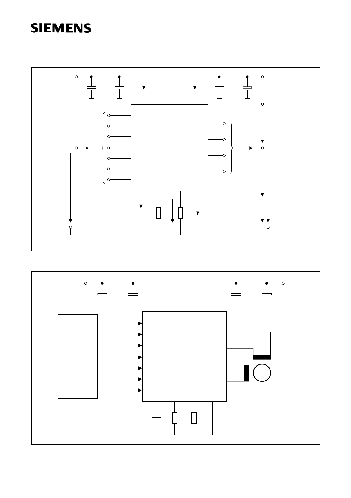
Figure 4 Test Circuit
220 nF100 F
1
Ι
2
Ι1011
3
Phase 1
17
Inhibit
20
19
ΙΙ21
18
Phase 2
Ι
OSCVOSC
2.2 nF
Ι
L
12 9
V
L
TCA 3727
20
413 8
R
2
Ω1
V
R
1Ω
Sense
Ι
S
V
S
Q11
Q12
Q21
Q22
220 nF 100 F
7
10
14
11
GNDOSC
µ
V
S
V
Satu
V
-
Ι
Q
Ι
-
Fu
-
Ι
R
Ι
Ru
V
Satl
Fu
V
-
Fl
5, 6
15, 16
V
1
Ι
GND
Sense
IES00706
µ
Micro
Controller
Figure 5 Application Circuit
220 nF100 F
1
10
Ι
2
Ι
11
3
Phase 1
17
Inhibit
20
Ι
20
19
Ι
21
18
Phase 2
2.2 nF
12 3
V
L
V
S
TCA 3727
GNDOSC
4138
R
R
2
Ω1
1
1Ω
Q11
Q12
Q21
Q22
5, 6
15, 16
220 nF 100 F
7
10
14
11
IES00707
+40 V+5 V
µ
M
Semiconductor Group 15 1998-02-01
Page 16
TCA 3727
Ι
10
Ι
11
Phase 1
Ι
Q1
i
i
i
acc
i
i
acc
acc
i
H
H
H
set
set
set
Accelerate Mode
Normal Mode
L
t
L
L
t
t
t
Ι
Q2
i
set
i
acc
H
Phase 2
Ι
20
Ι
21
L
H
L
H
L
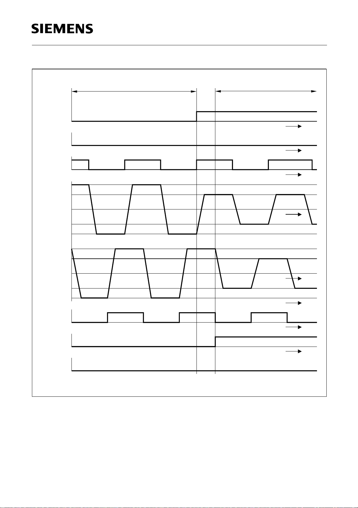
Figure 6 Full-Step Operation
t
t
t
t
IED01666
Semiconductor Group 16 1998-02-01
Page 17
TCA 3727
Ι
10
Ι
11
Phase 1
Ι
Q1
Accelerate Mode
Normal Mode
H
L
t
H
L
t
H
L
t
i
acc
i
set
t
-
i
set
-
i
acc
i
acc
i
set
Ι
Q2
-
i
set
-
i
acc
Phase 2
Ι
20
H
L
H
L
Ι
21
H
L
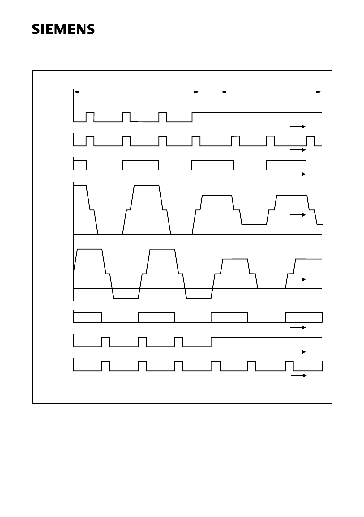
Figure 7 Half-Step Operation
t
t
t
t
IED01667
Semiconductor Group 17 1998-02-01
Page 18
TCA 3727
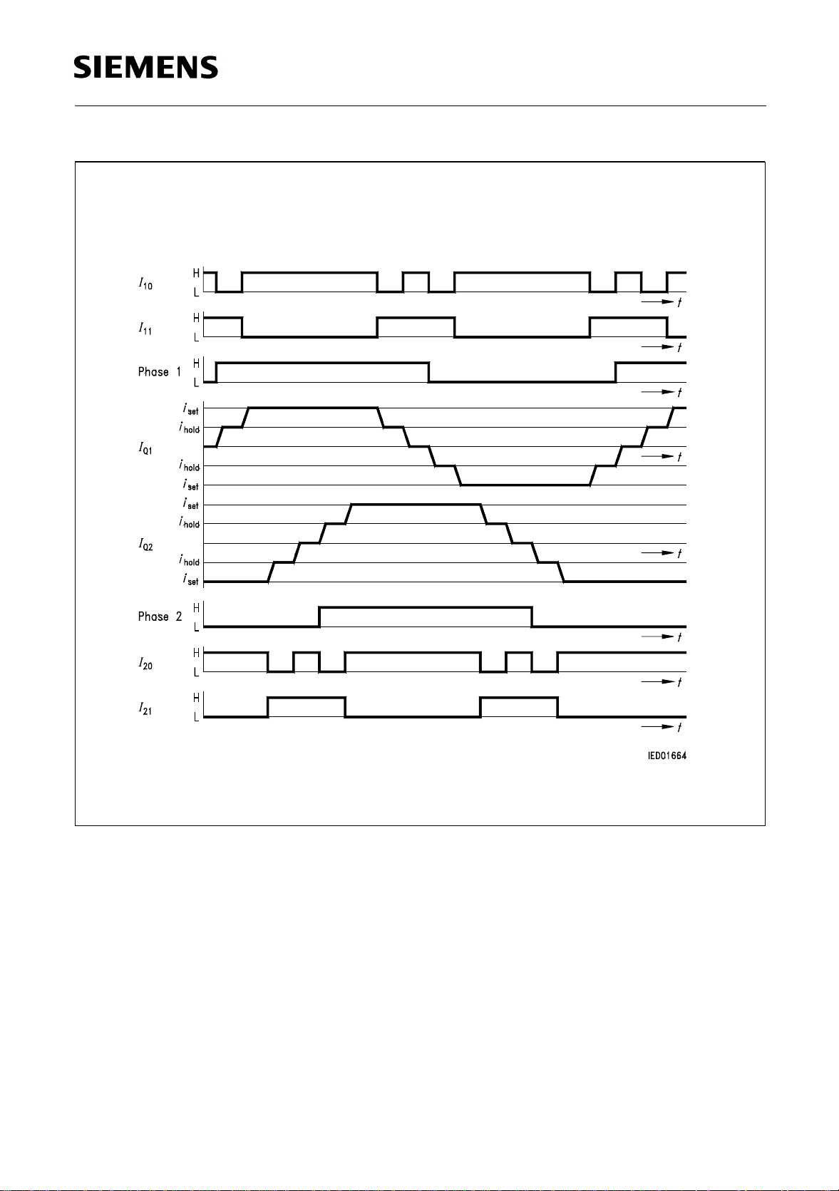
Figure 8 Quarter-Step Operation
Semiconductor Group 18 1998-02-01
Page 19
TCA 3727
Ι
10
Ι
11
Phase 1
Ι
Q1
Ι
Q2
i
i
i
hold
i
hold
i
i
i
i
i
hold
i
hold
i
i
H
L
t
H
L
t
H
L
t
acc
set
t
set
acc
acc
set
t
set
acc
Phase 2
H
L
Ι
20
Ι
21
H
L
H
L
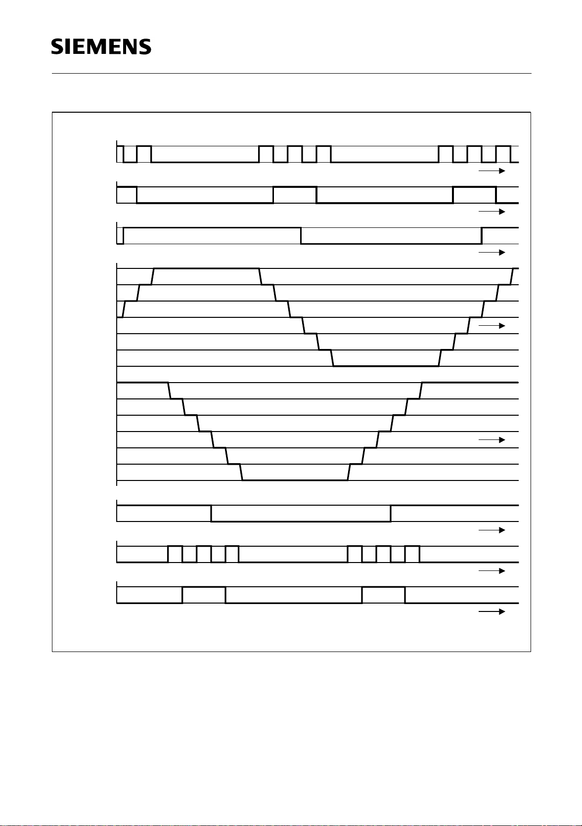
Figure 9 Mini-Step Operation
t
t
t
IED01665
Semiconductor Group 19 1998-02-01
Page 20
TCA 3727
V
Osc
2.4 V
1.4 V
Ι
GND
0
T
t
V
V
V
V
Q12
Q11
Q22
Q21
0
V
+
S
V
sat 1
V
FU
t
0
t
V
V
+
S
satu D
V
satu C
t
V
+
S
0
t
V
+
S
t
Operating conditions:
V
V
L
R
V
V
V
S
L
phase x
phase x
phase x
Inhibit
xx
= 40 V
= 5 V
= 10 mH
= 20
Ω
= H
= H
= L
IED01177
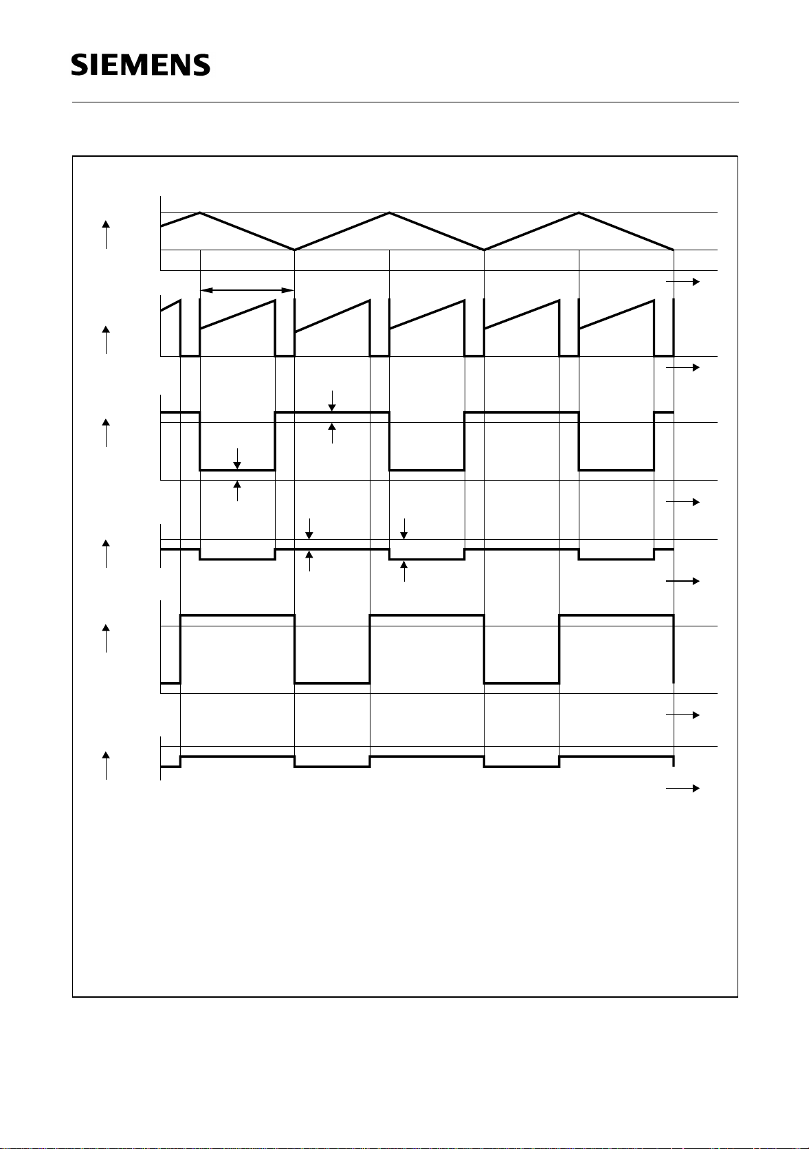
Figure 10 Current Control
Semiconductor Group 20 1998-02-01
Page 21
Inhibit
V
Osc
2.3 V
1.3 V
Phase 1
L
Oscillator
High Imped.
0
TCA 3727
t
Oscillator
High Imped.
t
Phase Changeover
Ι
V
V
GND
Q11
Q12
L
0
V
+
S
V
+
S
Ι
N
High
Impedance
High
Impedance
t
t
V
Fu
V
satu C
V
satu D
High
V
satl
Impedance
V
Fl
t
t
Ι
Phase 1
Operating Conditions:
phase 1
phase 1
= 40 V
= 5 V
= 10 mH
= 20
Ω
Ι
= L;
1X
= H
V
S
V
Ι
L
R
Ι
1X
Slow Current Decay
Fast Current Decay
Slow
Current Decay
t
Fast
Current
Decay by
Inhibit
IED01178
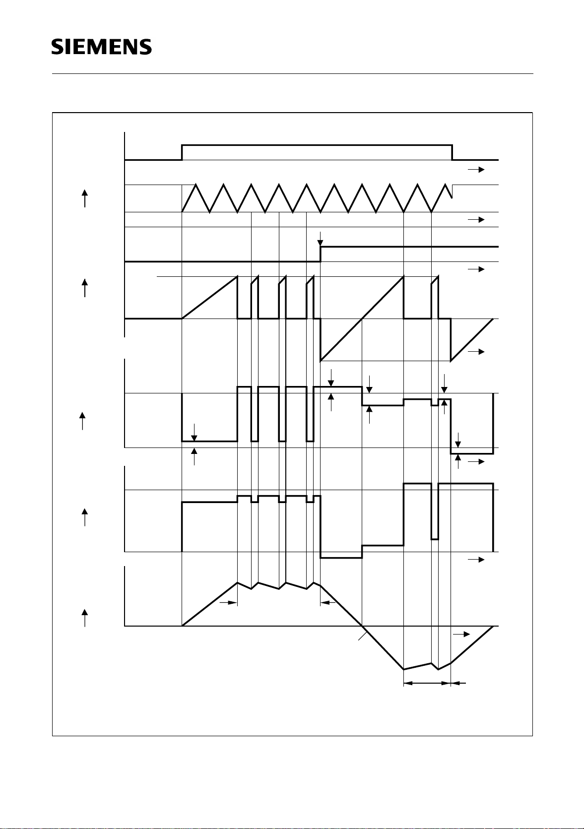
Figure 11 Phase Reversal and Inhibit
Semiconductor Group 21 1998-02-01
Page 22

TCA 3727
Calculation of Power Dissipation
P
The total power dissipation
P
P
P
sat
q
s
saturation losses
quiescent losses
switching losses
The following equations give the power dissipation for chopper operation without phase
reversal. This is the worst case, because full current flows for the entire time and
switching losses occur in addition.
P
= 2 × P
tot
where P
+ Pq + 2 × P
sat
≅ IN { V
sat
P
= Iq× VS + IL× V
q
V
S
------
≅
P
S
T
satl
i
t
×
D
DON
----------------------
2
is made up of
tot
(transistor saturation voltage and diode forward voltages),
(quiescent current times supply voltage) and
(turn-ON / turn-OFF operations).
s
× d + VFu (1 – d ) + V
L
iDi
+ tON×
R
----------------------------- -
4
I
---- -
2
N
t
DOFF
satuC
× d + V
t
+++
OFF
satuD
(1 – d ) }
I
N
I
q
i
D
i
R
t
p
t
ON
t
OFF
t
DON
t
DOFF
= nominal current (mean value)
= quiescent current
= reverse current during turn-on delay
= peak reverse current
= conducting time of chopper transistor
= turn-ON time
= turn-OFF time
= turn-ON delay
= turn-OFFdelay
T = cycle duration
d = duty cycle t
V
V
V
V
V
V
I
L
= saturation voltage of sink transistor (T3, T4)
satl
= saturation voltage of source transistor (T1, T2) during charge cycle
satuC
= saturation voltage of source transistor (T1, T2) during discharge cycle
satuD
= forward voltage of free-wheeling diode (D1, D2)
Fu
= supply voltage
S
= logic supply voltage
L
= current from logic supply
/T
p
Semiconductor Group 22 1998-02-01
Page 23
TCA 3727
+
V
S
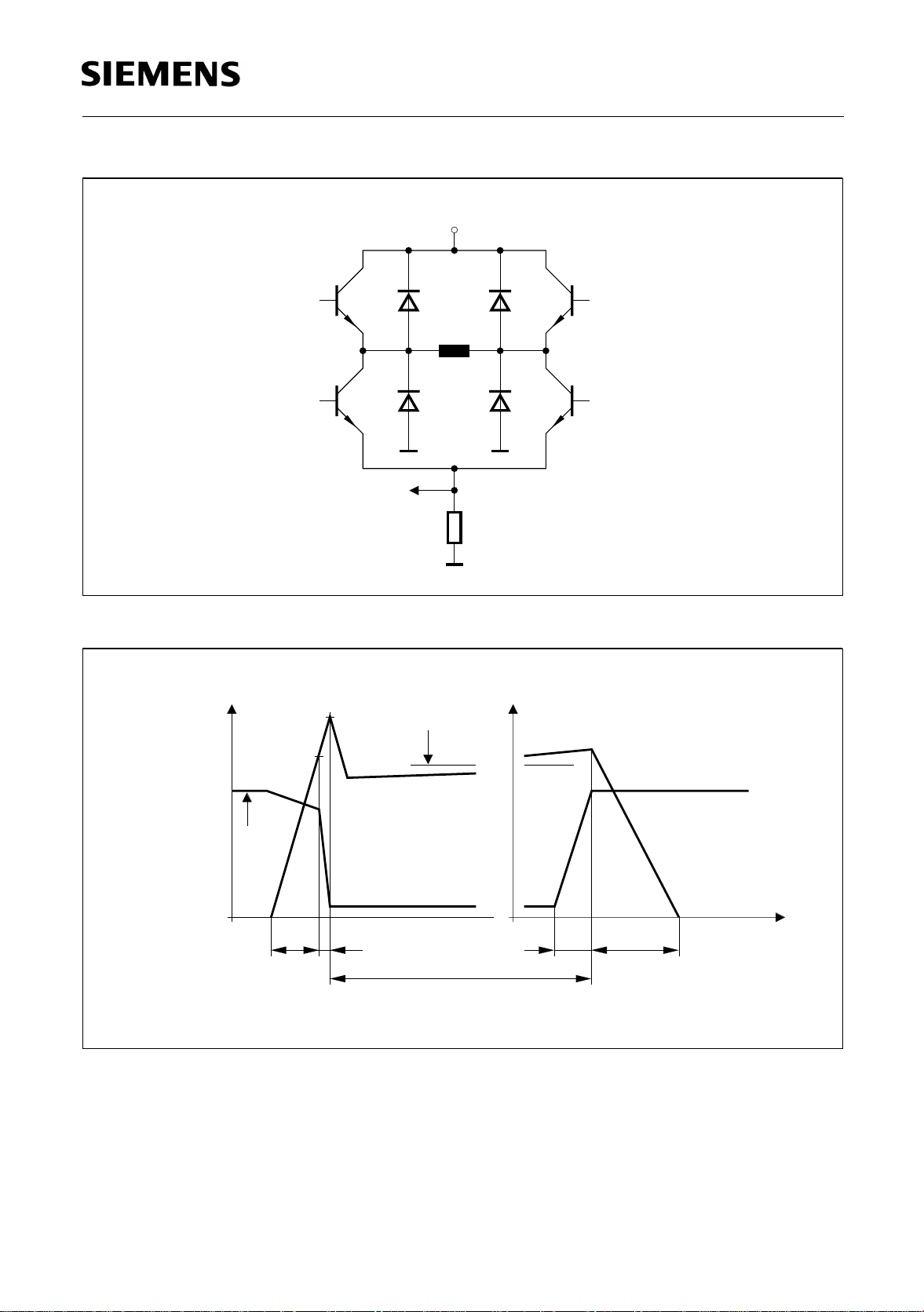
Figure 12
Voltage and
Current at
Chopper
Transistor
Tx1
Dx1 Dx2
Tx2
L
Tx3
V
sense
Turn-ON Turn-OFF
i
R
i
D
Dx3 Dx4
R
sense
Ι
N
Tx4
IES01179
+
V
V
FuS
+
V
V
SFu
V
satl
t
D
t
ON OFF
t
p
t
OFF
DON
t
t
IET01210
Figure 13
Semiconductor Group 23 1998-02-01
Page 24

TCA 3727
Application Hints
The TCA 3727 is intended to drive both phases of a stepper motor. Speci al care has
been taken to provide high efficiency, robustness and to minimize external components.
Power Supply
V
The TCA 3727 will work with supply vo ltag es ranging from 5 V to 50 V at pin
circuit operates with chopper regulation of the current, interference generation problems
can arise in some applicatio ns. Therefore the power supply should be decoupled by a
0.22 µF ceramic capacitor located near the pa ckage. Unstabilized supplies may even
afford higher capacities.
Current Sensing
. As the
s
The current in the windings of the stepper motor is sensed by the voltage drop across
R
and R2. Depending on the selected current internal compa rators will turn off the sink
transistor as soon as the vo ltage drop reaches certain thresholds (typ ical 0 V, 0.25 V,
R
0.5 V and 0.75 V); (
V
nor by variations of VS.
L
, R2=1 Ω). These thresholds are neither affected by variations of
1
Due to chopper control fast current rises (up to 10 A/µs) will occure at the sensing
R
resistors
and R2. To prevent malfunction of the current sensing mechanism R1 and R
1
should be pure oh mic. The resistors should be wired to G ND as directly as possible.
Capacitive loads such as long cables (with high wire to wire capacity) to the motor should
be avoided for the same reason.
Synchronizing Several Choppers
In some applications synchrone chopping of several stepper motor drivers may be
desireable to reduce aco ust ic i nterfe renc e. This can be done by forcing the o sci lla tor of
the TCA 3727 by a pulse generator overdriving the oscillator loading currents
(approximately Š± 100 µA). In these applica tions low level sho uld be between 0 V and
V
1 V while high level should be between 2.6 V and
.
L
Optimizing Noise Immunity
1
2
Unused inputs should always be wired to proper voltage levels in order to obtain highest
possible noise immunity.
To prevent crossconduction of the output stages the TCA 3727 uses a special break
before make timing of the power transistors. This timing circuit can be triggered by short
glitches (some hundred nano seconds) at the Phas e inputs causing the ou tput stage to
become high resis tive du ring some microsecon ds. Thi s w il l lead to a fast cu rre nt dec ay
during that time. To achieve maximum current accuracy such glitches at the Phase
inputs should be avoided by proper control signals.
Semiconductor Group 24 1998-02-01
Page 25

TCA 3727
Thermal Shut Down
To protect the circuit against thermal destruction, thermal shut down has been
implemented. To provide a warning in critical applications, the current of the sensing
element is wired to input Inhibit. Before thermal shut down occures Inhibit will start to pull
down by some hundred microamperes. This current can be sensed to build a
temperature prealarm.
Semiconductor Group 25 1998-02-01
Page 26
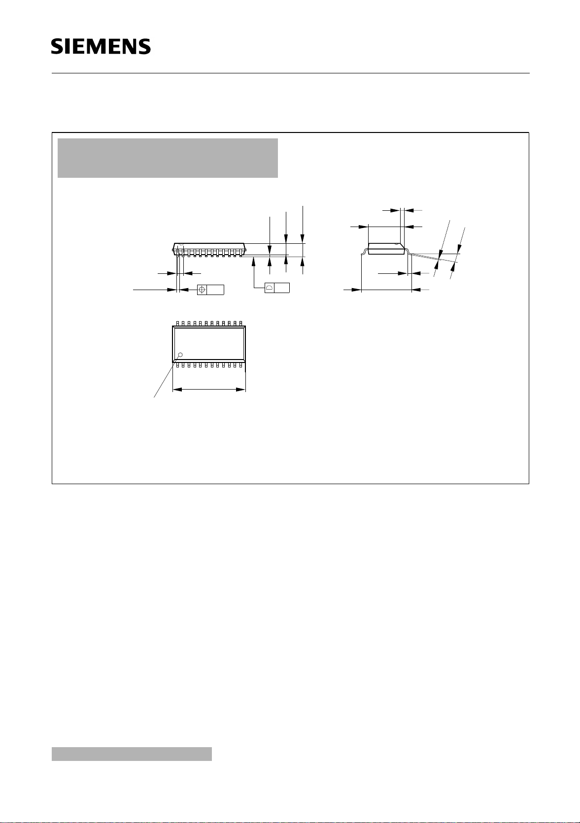
Package Outlines
P-DSO-24-3
(Plastic Dual Small Outline Package)
1.27
2)
+0.15
0.35
24 13
0.2 24x
-0.1
0.2
-0.2
2.45
0.1
2.65 max
0.35 x 45˚
7.6
-0.2
0.4
10.3
1)
+0.8
±0.3
+0.09
0.23
8˚ max
TCA 3727
112
15.6
-0.4
1)
Index Marking
1) Does not include plastic or metal protrusions of 0.15 max rer side
2) Does not include dambar protrusion of 0.05 max per side
GPS05144
Sorts of Packing
Package outlines for tubes, trays etc. are contained in our
Data Book “Package Information”.
SMD = Surface Mounted Device
Dimensions in mm
Semiconductor Group 26 1998-02-01
Page 27
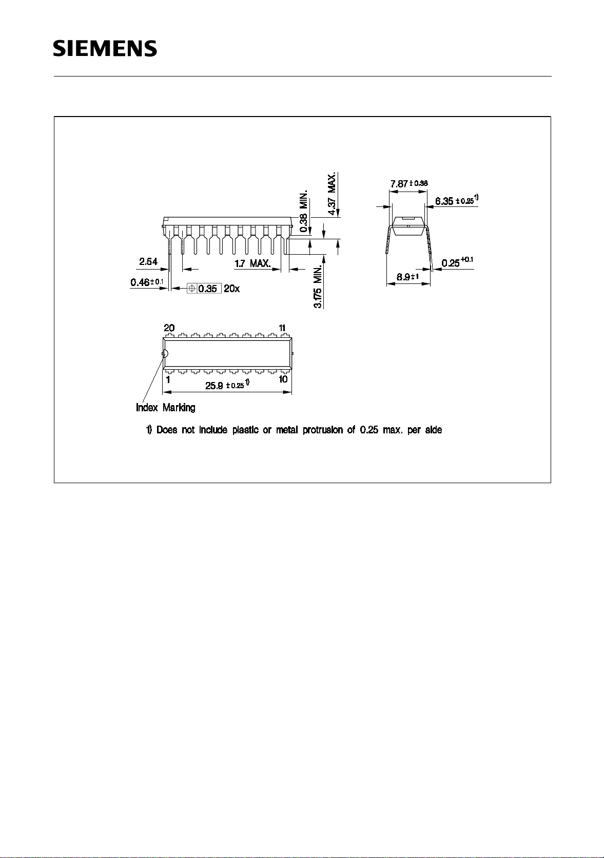
P-DIP-20-6
(Plastic Dual In-line Package)
TCA 3727
Sorts of Packing
Package outlines for tubes, trays etc. are contained in our
Data Book “Package Information”.
GPD05587
Dimensions in mm
Semiconductor Group 27 1998-02-01
 Loading...