

Page 1
Order this document by TCA5600/D
The TCA5600, TCF5600 are versatile power supply control circuits for
microprocessor based systems and are mainly intended for automotive
applications and battery powered instruments. To cover a wide range of
applications, the devices offer high circuit flexibility with a minimum of
external components.
Functions included in this IC are a temperature compensated voltage
reference, on–chip dc/dc converter, programmable and remote controlled
voltage regulator, fixed 5.0 V supply voltage regulator with external PNP
power device, undervoltage detection circuit, power–on RESET delay and
watchdog feature for safe and hazard free microprocessor operations.
• 6.0 V to 30 V Operation Range
• 2.5 V Reference Voltage Accessible for Other Tasks
• Fixed 5.0 V ± 4% Microprocessor Supply Regulator Including Current
Limitation, Overvoltage Protection and Undervoltage Monitor.
• Programmable 6.0 V to 30 V Voltage Regulator Exhibiting High Peak
Current (150mA), Current Limiting and Thermal Protection.
• Two Remote Inputs to Select the Regulator’s Operation Mode:
OFF = 5.0 V, 5.0 V Standby
Programmable Output Voltage
• Self–Contained dc/dc Converter Fully Controlled by the Programmable
Regulator to Guarantee Safe Operation Under All Working Conditions
• Programmable Power–On RESET Delay
• Watchdog Select Input
• Negative Edge Triggered W atchdog Input
• Low Current Consumption in the V
• All Digital Control Ports are TTL and MOS–Compatible
Applications Include:
• Microprocessor Systems with E
• High Voltage Crystal and Plasma Displays
• Decentralized Power Supplies in Computer Telecom Systems
CC1
2
PROMs
Standby Mode
UNIVERSAL
MICROPROCESSOR POWER
SUPPLY/CONTROLLERS
SEMICONDUCTOR
TECHNICAL DATA
18
1
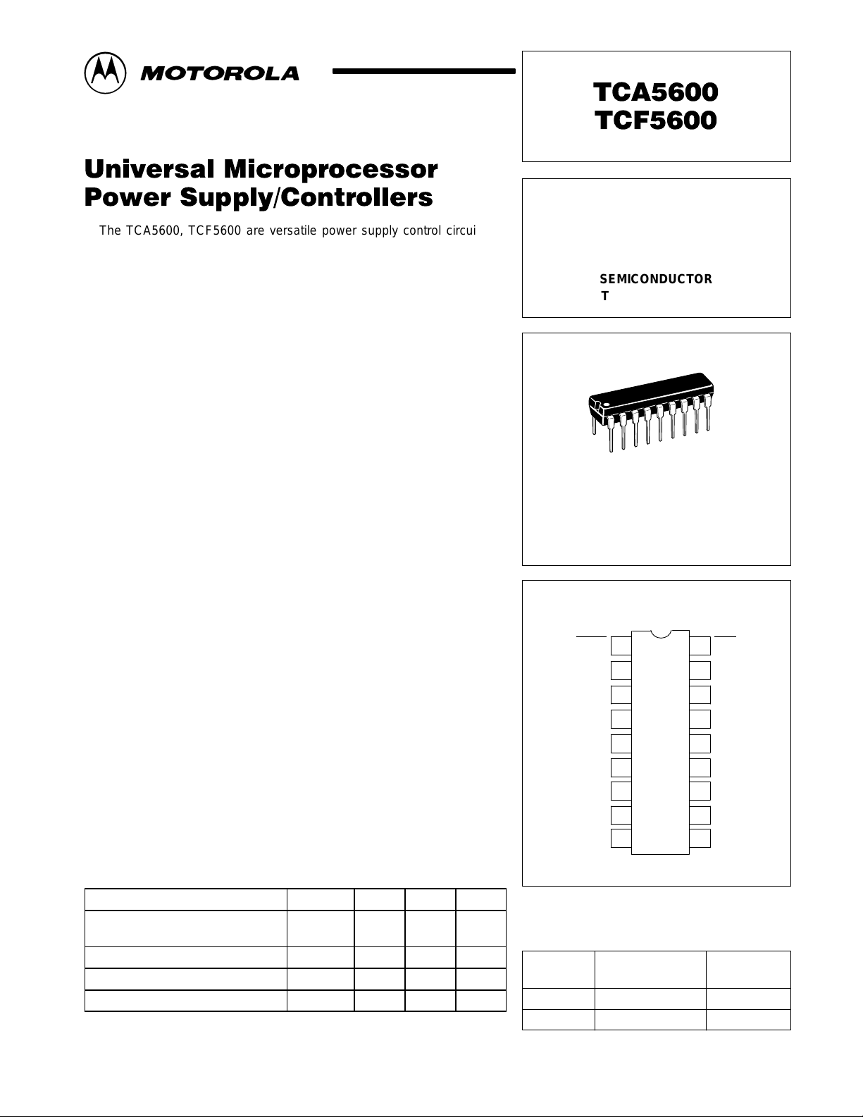
PLASTIC PACKAGE
CASE 707
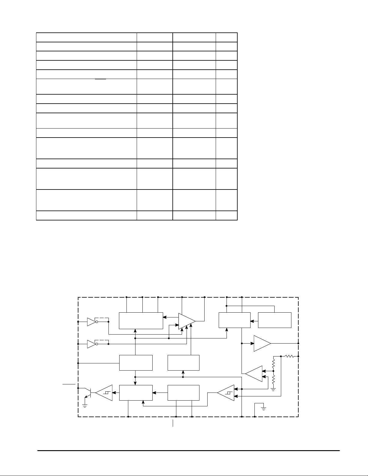
PIN CONNECTIONS
RESET
V
Sense
out1
V
CC1
WDI
V
ref
INH1
V
Prog
out2
V
Output
out2
Converter Output
1
2
3
4
5
6
7
8
9
WDS
18
Delay
17
I
Sense
16
out1
Base Drive
15
V
14
CC2
GND
13
Current Sense
12
INH2
11
Converter Input
10
RECOMMENDED OPERATING CONDITIONS
Characteristics Symbol Min Max Unit
Power Supply Voltage V
Collector Current I
Output Voltage V
Reference Source Current I
V
CC1
CC2
C
out2
ref
MOTOROLA ANALOG IC DEVICE DATA
5.0
5.5
— 800 mA
6.0 30 V
0 2.0 mA
30
30
(Top View)
V
ORDERING INFORMATION
Operating
Device
TCA5600
TCF5600
Motorola, Inc. 1996 Rev 0
Temperature Range
TJ = 0° to +125°C
TJ = – 40° to +150°C
Package
Plastic DIP
Plastic DIP
1
Page 2
MAXIMUM RATINGS
Power Supply Voltage (Pin 3,14) V
Base Drive Current (Pin 15) I
Collector Current (Pin 10) I
Forward Rectifier Current (Pin 10 to Pin 9) I
Logic Inputs INH1, INH2, WDS
(Pin 6, 11, 18)
Logic Input Current WDI (Pin 4) I
Output Sink Current RESET (Pin 1) I
Analog Inputs (Pin 2)
Analog Inputs (Pin 7)
Reference Source Current (Pin 5) I
Power Dissipation (Note 2)
TA = +75°C TCA5600
TA = +85°C TCF5600
Thermal Resistance, Junction–to–Air R
Operating Ambient Temperature Range
TCA5600
TCF5600
Operating Junction Temperature Range
TCA5600
TCF5600
Storage Temperature Range T
NOTES: 1. Values beyond which damage may occur.
2.Derate at 10 mW/°C for junction temperature above +75°C (TCA5600).
Derate at 10 mW/°C for junction temperature above +85°C (TCF5600).
(TA = +25°C [Note 1], unless otherwise noted.)
Rating Symbol Value Unit
CC1
V
WDI
RES
P
TCA5600 TCF5600
, V
B
C
F
INP
ref
D
θJA
T
A
T
stg
CC2
J
35 Vdc
20 mA
1.0 A
1.0 A
–0.3 V to V
–0.3 to 5.0
–40 to +85
–65 to +150 °C
CC1
±0.5 mA
10 mA
–0.3 to 10
5.0 mA
500
650
100 °C/W
0 to +75
+125
+150
Vdc
V
mW
°C
°C
Inhibit 2
(INH2)
Inhibit 1
(INH1)
Supply
Voltage V
RESET
CC1
11
6
3
1
Comp. II
Representative Block Diagram
CC2
Converter
Input
Converter
Output
Current
Sense VProgramming
10 9 12 7 8 14 16
DC/DC
Converter
Reference
2.5V
Delay Circuit
17
Delay
out2
A2
Thermal
Shut–Down
Watchdog
WDS
WDI
out2
Regulator
V
Comp. I
Supply
Voltage V
Current
Limit
Current
Sense
135418
ref
V
A1
A1
Gnd
Voltage
Protection
15
PNP Base Drive
2
V
Sense
out1
2
MOTOROLA ANALOG IC DEVICE DATA
Page 3
TCA5600 TCF5600
ELECTRICAL CHARACTERISTICS (V
Characteristics
= V
CC1
= 12 V; TJ = 25°C; I
CC2
INH2 = High; WDS
= High; I
= 0 [Note 4]; unless otherwise noted.)
out2
Figure Symbol Min Typ Max Unit
ref
REFERENCE SECTION
Nominal Reference Voltage 1 V
Reference Voltage
I
= 0.5 mA, T
ref
Line Regulation (6.0 V ≤ V
Average Temperature Coefficient
T
≤ TJ ≤ T
low
Ripple Rejection Ratio
f = 1.0 kHz, V
low
high
sin
≤ TJ ≤ T
(Note 5)
= 1.0 V
(Note 5), 6.0 V ≤ V
high
≤ 18 V) Reg
CC2
CC1
≤ 18 V
2 ∆V
3 RR 60 70 — dB
pp
Output Impedance
0 ≤ I
≤ 2.0 mA
ref
Standby Current Consumption
V
= Open
CC2
4 I
5.0 V MICROPROCESSOR VOLTAGE REGULATOR SECTION
Nominal Output Voltage V
Output Voltage
5.0 mA ≤ I
6.0 V ≤ V
Line Regulation (6.0 V ≤ V
Load Regulation (5.0 mA ≤ I
Base Current Drive (V
Ripple Rejection Ratio
f = 1.0 kHz, V
out1
CC2
≤ 18 V
sin
≤ 300 mA, T
CC2
= 6.0 V, V15 = 4.0 V) I
CC2
= 1.0 V
pp
low
≤ TJ ≤ T
high
(Note 5)
5
6
≤ 18 V) Reg
≤ 300 mA) Reg
out1
3 RR 50 65 — dB
Undervoltage Detection Level (RSC = 5.0 Ω) 7 V
Current Limitation Threshold (RSC = 5.0 Ω) V
Average Temperature Coefficient
T
low
≤ TJ ≤ T
high
(Note 5)
DC/DC CONVERTER SECTION
Collector Current Detection Level High
9 V12(H)
RC = 10 k Low
Collector Saturation Voltage
10 V
IC = 600 mA (Note 6)
Rectifier Forward Voltage Drop
11 V
IF = 600 mA (Note 6)
NOTES: 3. The external PNP power transistor satisfies the following minimum specifications:
hFE ≥ 60 at IC = 500 mA and VCE = 5.0 V;
V
≤ 300 mV at IB = 10 mA and IC = 300 mA
CE(sat)
4.Regulator V
5.T
= 0°C for TCA5600 T
low
T
= +125°C for TCA5600 T
high
6.Pulse tested tp ≤ 300 µs.
programmed for nominal 24 V output by means of R4, R5 (see Figure 1).
out2
= –40°C for TCF5600
low
= +150°C for TCF5600
high
= 0; I
out1
ref nom
V
ref
line
ref
∆T
J
Z
O
CC1
out1(nom)
V
out1
line
load
B
low
RSC
∆V
out1
∆T
J
V12(L)
CE(sat)
F
= 0 [Note 3]; RSC = 0.5 Ω; INH = High
2.42 2.5 2.58 V
2.4 — 2.6 V
— 2.0 15 mV
— — ±0.5 mV/°C
— 1.0 — Ω
— 3.0 — mA
4.8 5.0 5.2 V
4.75 — 5.25 V
— 10 50 mV
— 20 100 mV
10 15 — mA
4.5 0.93 × V
out1
— V
210 250 290 mV
— — ±1.0 mV/°C
350
—
400
50
450
—
— — 1.6 V
— — 1.4 V
mV
MOTOROLA ANALOG IC DEVICE DATA
3
Page 4
TCA5600 TCF5600
ELECTRICAL CHARACTERISTICS
ELECTRICAL CHARACTERISTICS INH2 = High; WDS = High; I
Characteristics
(V
CC1
= V
= 12 V; TJ = 25°C; I
CC2
ref
= 0 [Note 4]; unless otherwise noted.)
out2
Symbol Min Typ Max Unit
PROGRAMMABLE VOLTAGE REGULATOR SECTION (Note 6)
Nominal Output Voltage V
Output Voltage (Figure 8)
1.0 mA ≤ I
Load Regulation 1.0 mA ≤ I
≤ 100 mA, T
out2
≤ TJ ≤ T
low
≤ 100 mA (Note 7) Reg
out2
(Notes 5, 7)
high
out2(nom)
V
DC Output Current I
Peak Output Current (Internally Limited) I
out2 p
Ripple Rejection Ratio
f = 20 kHz, V = 0.4 V
Output Voltage (Fixed 5.0 V)
1.0 mA ≤ I
INH1 = HIGH (Note 5)
out2
pp
≤ 20 mA, T
low
≤ TJ ≤ T
high
V
out2(5.0 V)
Off State Output Impedance (INH2 = Low) R
Average Temperature Coefficient
T
low
≤ TJ ≤ T
high
(Note 5)
∆V
∆TJV
WATCHDOG AND RESET CIRCUIT SECTION
Threshold Voltage High
(Static) Low
Current Source T
Power–Up RESET
low
≤ TJ ≤ T
high
(Note 5)
V
V
Watchdog Time Out
Watchdog RESET
Watchdog Input V oltage Swing V
Watchdog Input Impedance r
Watchdog Reset Pulse Width (C8 = 1.0 nF) (Note 9) t
DIGITAL PORTS: WDS, INH 1, INH 2, RESET (Note 8)
Input Voltage Range V
Input High Current
2.0 V ≤ VIH ≤ 5.5 V
5.5 V ≤ VIH ≤ V
CC1
Input Low Current
–0.3 V ≤ VIL ≤ 0.8 V for INH1, INH2, –0.3 V ≤ VIL ≤ 0.4 V for WDS
Leakage Current Immunity (INH2, High “Z” State) (Figure 12) I
Output Low Voltage RESET (IOL = 6.0 mA) V
Output High Voltage RESET (VOH = 5.5 V) V
NOTES: 3. The external PNP power transistor satisfies the following minimum specifications:
hFE ≥ 60 at IC = 500 mA and VCE = 5.0 V;
V
≤ 300 mV at IB = 10 mA and IC = 300 mA
CE(sat)
4.Regulator V
5.T
= 0°C for TCA5600 T
low
T
= +125°C for TCA5600 T
high
6.V9 = 28 V, INH1 = LOW for this Electrical Characteristic section unless otherwise noted.
7.Pulse tested tp ≤ 300 µs.
8.Temperature range T
9.For test purposes, a negative pulse is applied to Pin 4 (–2.5 V ≥ V4 ≥ –5.5 V).
programmed for nominal 24 V output by means of R4, R5 (see Figure 1).
out2
low
≤ TJ ≤ T
= –40°C for TCF5600
low
= +150°C for TCF5600
high
applies to this Electrical Characteristics section.
high
= 0; I
= 0 [Note 3]; RSC = 0.5 Ω; INH = High
out1
23 24 25 V
out2
load
out2
22.8 — 25.2 V
— 40 200 mV
100 — — mA
150 200 — mA
RR 45 55 — dB
4.75 — 5.25 V
out1
out2
— 10 — kΩ
— — ±0.25 mV/°C V
out2
C5(H)
C5(L)
I
C5
WDI
i
p
INP
I
IH
I
IL
Z
OL
OH
—
—
–1.8
—
—
— — ±5.5 V
12 15 — kΩ
— — 10 µs
— — –0.3 to V
—
—
— — –100
±20 — — µA
— — 0.4 V
— — 20 µA
2.5
1.0
–2.5
5×I
–50×I
—
—
C5
C5
—
—
–3.2
—
—
CC1
100
150
V
µA
V
µA
µA
4
MOTOROLA ANALOG IC DEVICE DATA
Page 5

Figure 1. Reference V oltage versus Supply Voltage
2.4
2.0
1.6
1.2
, REFERENCE VOLTAGE (V)
0.8
0.4
ref nom
V
0
1.0 2.0 3.0 4.0 5.0 10 20 30 40
V
, SUPPLY VOLTAGE (V)
CC1
Figure 2. Reference Stability versus T emperature
TCA5600 TCF5600
V
CC1
+
NC
NC
NC
61118
3
12
4
NC NC
V
out2
86k
10k
R4
R5
10
V
914
ref nom
R
SC
Ω
0.5
16
µ
F
Q1
BD242SP
V
out1
+
C410
15
2
15781317
60
40
20
+0
–20
, VOLTAGE DRIFT (mV)
ref
–40
V
∆
–60
–50 –25 0 25 50 75 100 125 150
TJ, JUNCTION TEMPERATURE (
TCA5600
TCF5600
°
C)
Figure 3. Ripple Rejection versus Frequency
70
60
50
40
30
20
10
RR, RIPPLE REJECTION RATIO (dB)
0
1.0 k 10 k 100 k 1.0 M
V
out1
f,FREQUENCY (Hz)
V
ref
V
+
Ω
= 1.0 V
150
+
V
CC1
CC1
R3
Ω
61118
3
12
NC
4
NC
NC NC
V
out2
PP
0.33µF
C6
61118
3
12
NC
4
NC
NC NC
V
out2
R4
86k
R5
10k
R4
86k
R5
10k
NC
10
∆
NC
10
914
15781317
V
ref
914
15781317
V
ref nom
16
15
16
15
R
SC
Ω
0.5
Q1
BD242SP
2
µ
F
+
V
nom
ref
R
SC
0.5
Ω
2
µ
+
C410
Q1
BD242SP
+
F
V
out1
V
out1
C410
MOTOROLA ANALOG IC DEVICE DATA
5
Page 6

TCA5600 TCF5600
Figure 4. Standby Current versus Supply V oltage
6
5
4
3
2
, STAND–BY CURRENT (mA)
CC1
I
1
0
6
5
4
3
2
, OUTPUT VOL TAGE (V)
out1
1
V
0
2.0 3.01.0 4.0 5.0 10 20 30 40
V
, SUPPLY VOLTAGE (IV)
CC1
Figure 5. Power–Up Behavior of the 5.0 V Regulator
I
= 300 mA
out
2.0 3.01.0 4.0 5.0 10 20 30 40
V
, SUPPLY VOLTAGE (IV)
CC2
R
I
V
CC1
CC1
+
V
CC1
+
61118
3
12
NC
4
NC
NC NC
V
out2
61118
3
12
NC
4
NC
NC NC
V
out2
R4
86k
R5
10k
R4
86k
R5
10k
NC
10
NC
10
914
15781317
V
ref
914
15781317
16.7
R
out1
V
ref
SC
Ω
0.5
16
R
0.5
µ
SC
I
out1
Q1
BD242SP
+
F
Ω
Q1
BD242SP
+
C410
C4
10
V
out1
V
out1
µ
F
15
2
16
15
2
Ω
Figure 6. Foldback Characteristics of the 5.0 V Regulator
7.0
6.0
5.0
4.0
3.0
, SUPPLY VOLTAGE (V)
2.0
CC2
1.0
V
0
0 100 200 300 400 500 600
28 V 24 V
I
, OUTPUT CURRENT (mA)
out1
6
V
CC2
≤20 V
R
16
15
SC
0.5
Ω
Q1
BD242SP
2
I
out1
100
Ω
V
out1
+
C4
µ
F
10
R4
86k
R5
10k
NC
10
914
15781317
R
out1
V
ref
V
CC1
+
+
V
CC1
61118
3
12
NC
4
NC
NC NC
V
out2
MOTOROLA ANALOG IC DEVICE DATA
Page 7

TCA5600 TCF5600
Figure 7. Undervoltage Lockout Characteristics
7
6
5
4
3
, RESET VOL TAGE (V)
2
RES
V
1
0
0 1.0 2.0 3.0 4.0 5.0 6.0 7.0 8.0
V
, OUTPUT VOLTAGE (V)
out1
Figure 8. Output Current Capability of the Programming Regulator
28
24
20
16
12
, SUPPLY VOLTAGE (V)
8.0
g
V
4.0
0
0 20 40 60 80 100 120 140 160
I
, OUTPUT CURRENT (mA)
out2
R
16
15
16
15
2
R6
10k
2
0.5
R
0.5
SC
SC
µ
Ω
Q1
BD242SP
Ω
Q1
BD242SP
F
V
out1
+
C4
10
µ
F
V
out1
+
C410
R4
86k
R5
10k
R4
86k
R5
10k
NC
10
V
NC
10
914
15781317
RESET
ref
914
15781317
V
ref
V
CC1
+
+
V
9
+
V
CC1
R
61118
3
12
NC
4
NC
NC
V
out2
61118
3
12
NC
4
NC
NC NC
I
out2
out2
5.0k
C3
47nF
Figure 9. Collector Current Detection Level
16
12
8.0
, COLLECTOR VOLTAGE (V)V
4.0
10
0
V
12(L)
0 100 200 300 400 500
V
CURRENT SENSE VOLTAGE (mV)
12,
V
MOTOROLA ANALOG IC DEVICE DATA
12(H)
10k
R
R4
86k
R5
10k
10
C
V
ref
V
+
V
CC1
V
12
61118 914
3
12
4
NC
NC NC
V
out2
10
R
SC
Ω
0.5
16
µ
F
Q1
BD242SP
V
out1
+
C410
15
2
15781317
7
Page 8

Figure 10. Power Switch Characteristics
1.8
1.6
1.4
1.2
, SATURATION VOLTAGE (V)
1.0
CE(sat)
0.8
V
0.6
10 20 30 50 80 100 200 300 500 800
I
, COLLECTOR CURRENT (mA)
C10
Figure 11. Rectifier Characteristics
1.8
1.6
1.4
1.2
1.0
, FORWARD VOLTAGE (V)
F
V
0.8
0.6
10 20 30 50 80 100 200 300 500 800
IF,
RECTIFIER CURRENT (mA)
TCA5600 TCF5600
V
CC1
+
NC
V
CC1
+
NC
NC
61118 914
3
12
4
NC NC
V
out2
61118 914
3
12
4
NC NC
V
out2
R4
86k
R5
10k
R4
86k
R5
10k
10
10
15781317
V
ref
15781317
V
ref
I
C10
16
15
2
16
15
2
R
0.5
R
0.5
SC
µ
SC
µ
Ω
Q1
BD242SP
F
Ω
Q1
BD242SP
F
V
out1
+
C410
I
F
V
out1
+
C410
Figure 12. INH 2 Leakage Current Immunity
28
24
20
16
12
, OUTPUT VOL TAGE (V)V
8.0
out2
4.0
0
–40 –30 –20 –10 0 10 20 30 40
IZ, LEAKAGE CURRENT (
V
out2
Spec Limits
High “Z” State
V
10
µ
A)
8
V
CC1
10k
R
R4
86k
R5
10k
10
C
V
ref
V
+
I
Z
61118 914
3
12
4
NC
NC NC
V
out2
C3
47nF
10
R
SC
Ω
0.5
16
15
2
15781317
Q1
BD242SP
V
out1
+
C410µF
V
g
MOTOROLA ANALOG IC DEVICE DATA
Page 9

TCA5600 TCF5600
(
)
(H)
APPLICATIONS INFORMATION
(See Figure 18)
V oltage Reference (V
The voltage reference V
)
ref
is based upon a highly stable
ref
bandgap voltage reference and is accessible on Pin 5 for
additional tasks. This circuit part has its own supply
connection on Pin 3 and is, therefore, able to operate in
standby mode. The RC network R3, C6 improves the ripple
rejection on both regulators.
DC/DC Converter
The dc/dc converter performs according to the flyback
principle and does not need a time base circuit. The
maximum coil current is well defined by means of the current
sensing resistor R1 under all working conditions (startup
phase, circuit overload, wide supply voltage range and
extreme load current change). Figure 13 shows the Simplified
Converter Schematic.
Figure 13. Simplified Converter Schematic
V
V
V
12(H)
12(L)
Control Feedback
+
CC2
Comp
0.68
R1
L1
µ
H
300
10
R4
85K
V
out2
C3
47nF
VF
V
CE(sat)
C2
100
+
µ
12
Ω
Prog.
Regulator
9
F
C7
0.22µF
8
7
R5
10k
A simplified method on “how to calculate the coil inductance”
is given below. The operation point at minimum supply
voltage (V
output voltage (V
) and max. output current (I
CC2
) determines the coil data. Figure 14
out2
) for a fixed
out2
shows the typical voltage and current waveforms on the coil
L1 (coil losses neglected).
Equations (1) and (2) yield the respective coil voltage
VL– and VL + (see Figure 14):
VL+ = V
VL– = V
[∆V
(Pin 9 – Pin 8)
out2
+ ∆V
CC2
(Pin 9 – Pin 8)
– V
CE
+ VF – V
– V
sat
CC2
12
: input/output voltage drop of the regulator,
(1)
(2)
2.5 V typical]
[VF, V
CE(sat)
, V
: see Electrical Characteristics Table]
12(H)
The time ratio α for the charging time to dumping time is
defined by Equation (3):
t
VL+
α =
1
=
t
VL–
2
(3)
Figure 14. V oltage and Current Waveform
on the Coil (not to scale)
Coil
Voltage
V
CC2
Coil
Current
I
Lpeak
t
t
1
2
+
L
V–
L
V
t
t
The coil charging time t1 is found using Equation (4):
(1 +
1
1
) ⋅ f
α
(4)
t1 =
[f : minimum oscillation frequency which should be chosen
above the audio frequency band (e.g. 20 kHz)]
Knowing the dc output current I
regulator, the peak coil current I
I
L(peak)
= 2 ⋅ (I
of the programmable
out2
can now be calculated:
L(peak)
) (1 + α)
out2
(5)
The coil inductance L1 of the nonsaturated coil is given by
Equation (6):
t
1
I
L(peak)
(VL–)
(6)L1 =
The formula (6a) yields the current sensing resistor R1 for a
defined peak coil current I
R1 =
L(peak)
V
12(H)
I
L(peak)
:
(6a)
In order to limit the by–pass current through capacitor C7
during the energy dumping phase the value C2>>C7 should
be implemented.
For all other operation conditions, the feedback signal from
the programmable voltage regulator controls the activity of
the converter.
MOTOROLA ANALOG IC DEVICE DATA
9
Page 10

TCA5600 TCF5600
Programmable V oltage Regulator
This series voltage regulator is programmable by the
voltage divider R4, R5 for a nominal output voltage of 6.0 V ≤
V
≤ 30 V.
out2
(V
R4 =
out2
[R5 = 10 k, V
– V
ref nom
V
ref nom
ref nom
)
• R5
= 2.5 V]
(7)
Current limitation and thermal shutdown capability are
standard features of this regulator. The voltage drop
∆V
(Pin 9 – Pin 8)
across the series pass transistor generates
the feedback signal to control the dc/dc converter
(see Figure 13).
Control Inputs INH1, INH2
The dc/dc converter and/or the regulator V
are remote
out2
controllable through the TTL, MOS compatible inhibit inputs
INH1 and INH2 where the latter is a three–level detector
(Logic “0”, High Impedance “Z”, Logic “1”). Both inputs are
set–up to provide the following truth table:
Figure 15. INH1, INH2 TruthTable
Mode INH1 INH2 V
1 0 0 OFF INT
2 0 High “Z” V
3 0 1 V
4 1 0 OFF INT
5 1 High “Z” 5.0 V ON
6 1 1 5.0 V INT
INT: Intermittent operation of the converter means that the
converter operates only if V
ON: The converter loads the storage capacitor C2 to its full
charge (V9 = 33 V), allowing fast response time of the
regulator V
OFF: High impedance (internal resistor 10 k to ground)
when addressed by the control software.
out2
out2
out2
out2
CC2<Vout2
DC/DC
ON
INT
.
Microprocessor Supply Regulator
Together with an external PNP power transistor (Q1), a
5.0 V supply exhibiting low voltage drop is obtained to power
microprocessor systems and auxiliary circuits. Using a power
Darlington with adequate heat sink in the output stage boosts
the output current I
above 1.0 A.
out1
The current limitation circuit measures the emitter current
of Q1 by means of the sensing resistor, RSC:
V
RSC
I
E
(8)RSC =
[IE: emitter current of Q1]
[V
: threshold voltage
RSC
[V
: (see Electrical Characteristics Table)]
RSC
The voltage protection circuit performs a foldback
characteristic above a nominal operating voltage, V
CC2
≥
18 V.
Delay and Watchdog Circuit
The undervoltage monitor supervises the power supply
V
and releases the delay circuit RESET
out1
as soon as the
regulator output reaches the microprocessor operating a
range [e.g., V
low
w 0.93
• V
out1(nom)
]. The RESET output has
an open–collector and may be connected in a “wired–OR”
configuration.
The watchdog circuit consists of a retriggerable
monostable with a negative edge sensitive control input WDI.
The watchdog feature may be disabled by means of the
watchdog select input WDS
the Typical RESET
Timing Diagram.
driven to a “1”. Figure 17 displays
The commuted current source IC5 on Pin 17, threshold
voltage V
the RESET
C5(L)
, V
and an external capacitor C5 define
C5(H)
delay and the watchdog timing. The relationship
of the timing signals are indicated by the Equations (9) to (1 1).
Figure 16 represents a typical timing diagram for an E2PROM
programming sequence in a microprocessor based system.
The High “Z” state enables the dc/dc converter to ramp during
t3 to the voltage V9 at Pin 9 to a high level before the write
cycle takes place in the memory.
Figure 16. T ypical E2PROM Programming Sequence
(not to scale)
V9
– V
F
High “Z”
max
t3t
4
V9
int
Programming
Voltage VPP
t
V
CC2
V
out2
5.0V
INH1
“1”
”0”
INH2
“1”
“0”
V
9
delay: td =
Watchdog timeout:
Watchdog RESET:
[IC5, V
C5(H)
, V
C5(L)
C5
• V
C5(H)
|IC5|
twd =
tr =
C5 • (V
C5 • (V
C5(H)
50
C5(H)
5
• I
• |I
C5
C5
– V
– V
|
C5(L)
C5(L)
)
(10)
)
(11)
: see Electrical Characteristics Table]
(9)RESET
10
MOTOROLA ANALOG IC DEVICE DATA
Page 11

V
CC2
TCA5600 TCF5600
Figure 17. T ypical RESET Timing Diagram (not to scale)
V
< V
CC2
out1
MR752
V
bat
R3
150
D1
Ω
V
out1
(a)
V
C5
RESET
V
C5
WDI
(b)
RESET
V
Ignition
Key
C1
µ
220
Z1
MR2525L
Overload
C5(N)
t
d
V
C5(L)
t
wd
V
t
r
Figure 18. T ypical Automative Application
100µF
R1
0.68
C2
Ω
300
F
+
µ
H
L1
V
D
10 9 8
0.22
C7
712
86k
µ
F
R5
10k
C5(H)
R4
+
47
nF
C3
V
out2
50mA
V
CC2
24V
14
R2
0.5
(a) Watchdog inhibited, WDS
(b) Watchdog operational, WDS
Ω
16
= “1”
= “0”
µ
µ
C6
0.33
P
C9
22nF
P
V
CC1
µ
F
INH
INH
RESET
µ
P
2
11
6
1
3
1
DC/DC
Converter
Reference
2.5V
Delay
Circuit
17 4 5 13
IC 5
C5
100nF
A2
Thermal
Shut–Down
Watchdog
18
WDS
µ
TCA5600
WDI
C8
330pF
P
Current
Limit
V
ref
A1
Protection
Gnd
Voltage
A1
15
2
Q1*
BD242SP
µ
150
V
out1
5.0V/300mA
F+
C4
MOTOROLA ANALOG IC DEVICE DATA
11
Page 12

TCA5600 TCF5600
OUTLINE DIMENSIONS
PLASTIC PACKAGE
CASE 707–02
ISSUE C
18
10
B
1
9
A
C
K
N
F
D
H
G
SEATING
PLANE
L
M
J
NOTES:
1. POSITIONAL TOLERANCE OF LEADS (D),
SHALL BE WITHIN 0.25 (0.010) AT MAXIMUM
MATERIAL CONDITION, IN RELATION TO
SEATING PLANE AND EACH OTHER.
2. DIMENSION L TO CENTER OF LEADS WHEN
FORMED PARALLEL.
3. DIMENSION B DOES NOT INCLUDE MOLD
FLASH.
DIM MIN MAX MIN MAX
A 22.22 23.24 0.875 0.915
B 6.10 6.60 0.240 0.260
C 3.56 4.57 0.140 0.180
D 0.36 0.56 0.014 0.022
F 1.27 1.78 0.050 0.070
G 2.54 BSC 0.100 BSC
H 1.02 1.52 0.040 0.060
J 0.20 0.30 0.008 0.012
K 2.92 3.43 0.115 0.135
L 7.62 BSC 0.300 BSC
M 0 15 0 15
__ __
N 0.51 1.02 0.020 0.040
INCHESMILLIMETERS
Motorola reserves the right to make changes without further notice to any products herein. Motorola makes no warranty , representation or guarantee regarding
the suitability of its products for any particular purpose, nor does Motorola assume any liability arising out of the application or use of any product or circuit, and
specifically disclaims any and all liability, including without limitation consequential or incidental damages. “T ypical” parameters which may be provided in Motorola
data sheets and/or specifications can and do vary in different applications and actual performance may vary over time. All operating parameters, including “Typicals”
must be validated for each customer application by customer’s technical experts. Motorola does not convey any license under its patent rights nor the rights of
others. Motorola products are not designed, intended, or authorized for use as components in systems intended for surgical implant into the body, or other
applications intended to support or sustain life, or for any other application in which the failure of the Motorola product could create a situation where personal injury
or death may occur. Should Buyer purchase or use Motorola products for any such unintended or unauthorized application, Buyer shall indemnify and hold Motorola
and its officers, employees, subsidiaries, affiliates, and distributors harmless against all claims, costs, damages, and expenses, and reasonable attorney fees
arising out of, directly or indirectly, any claim of personal injury or death associated with such unintended or unauthorized use, even if such claim alleges that Motorola
was negligent regarding the design or manufacture of the part. Motorola and are registered trademarks of Motorola, Inc. Motorola, Inc. is an Equal
Opportunity/Affirmative Action Employer.
How to reach us:
USA/EUROPE /Locations Not Listed: Motorola Literature Distribution; JAPAN: Nippon Motorola Ltd.; Tatsumi–SPD–JLDC, 6F Seibu–Butsuryu–Center,
P.O. Box 20912; Phoenix, Arizona 85036. 1–800–441–2447 or 602–303–5454 3–14–2 Tatsumi Koto–Ku, Tokyo 135, Japan. 03–81–3521–8315
MFAX: RMF AX0@email.sps.mot.com – TOUCHT ONE 602–244–6609 ASIA/PACIFIC: Motorola Semiconductors H.K. Ltd.; 8B Tai Ping Industrial Park,
INTERNET: http://Design–NET.com 51 Ting Kok Road, Tai Po, N.T., Hong Kong. 852–26629298
12
◊
MOTOROLA ANALOG IC DEVICE DATA
TCA5600/D
*TCA5600/D*
 Loading...