

Page 1
Order this document by TCA3388/D
The TCA3388 is a telephone line interface circuit which performs the basic
functions of a telephone set in combination with a microcontroller and a ringer.
It includes dc and ac line termination, the hybrid function with 2 adjustable
sidetone networks, handset connections and an efficient supply point.
FEATURES
Line Driver and Supply
• DC and AC Termination of the Telephone Line
• Selectable DC Mask: France, U.K., Low Voltage
• Current Protection
• Adjustable Set Impedance for Resistive and Complex Termination
• Efficient Supply Point for Peripherals
• Hook Status Detection
Handset Operation
• Transmit and Receive Amplifiers
• Double Anti–Sidetone Network
• Line Length AGC
• Microphone and Earpiece Mute
• Transmit Amplifier Soft Clipping
Dialing and Ringing
• Interrupter Driver for Pulse–Dialing
• Reduced Current Consumption During Pulse–Dialing
• DTMF Interfacing
• Ringing via External Ringer
TELEPHONE LINE
INTERFACE
SEMICONDUCTOR
TECHNICAL DATA
20
1
DP SUFFIX
PLASTIC PACKAGE
CASE 738
20
1
FP SUFFIX
PLASTIC PACKAGE
CASE 751D
PIN CONNECTIONS
Application Areas
• Corded Telephony
• Cordless Telephony Base Station
• Answering Machines
• Fax
• Intercom
• Modem
This document contains information on a new product. Specifications and information herein
are subject to change without notice.
MOTOROLA ANALOG IC DEVICE DATA
120
RXI
2
TXI
3
Mic
4
LAO
5
LAI
6
HYL
7
HYS
8
CM
9
IMP
SAO SAI
ORDERING INFORMATION
Device
TCA3388DP
TCA3388FP
Motorola, Inc. 1995
Temperature Range
(Top View)
Tested Operating
TA = 0° to +70°C
19
18
17
16
15
14
13
12
1110
RXO2
RXO1
Gnd
V
CC
I
ref
MUT
PI
HSO
DCM
Package
DIP
SOIC
1
Page 2
TCA3388
ÁÁÁ
ÁÁÁ
ÁÁÁ
ÁÁÁ
ÁÁÁ
ÁÁÁ
Simplified Block Diagram
DC and AC
Termination
Line +
Handset
Earpiece
Handset
MIcrophone
Ear
Mic
DC Mask Generation
AC Termination
2–4 Wire Conversion
Microcontroller
Interface
This device contains 1,911 active transistors.
MAXIMUM RATINGS
Rating Symbol Min Max Unit
Maximum Junction Temperature T
Storage Temperature Range T
NOTE: Devices should not be operated at or outside these values. The “Recommended Operating
Limits” provide for actual device operation.
J
stg
– +150 °C
–65 +150 °C
RECOMMENDED OPERATING CONDITIONS
Characteristic Symbol Min Typ Max Unit
Operating Temperature Range T
A
0 – +70 °C
Supply
Stabilizer
Line Driver
Line –
DC ELECTRICAL CHARACTERISTICS (T
Characteristic
= 25°C)
A
Symbol Min Typ Max Unit
VOLTAGE REGULATOR
Regulated Supply at Pin 17 V
CC
ICC = 7.0 mA 3.4 3.7 4.0
ICC = 20 mA 3.45 3.75 4.05
ICC = 80 mA 3.5 3.8 4.1
Current Consumption at Pin 17, Pin PI = High I
CC
– – 600 µA
DRIVER DC CHARACTERISTICS
Available Current at LAO
I4
Source Current 45 70 100
Sink Current –100 –70 –45
Amplifier A8 Driver Slope
LAO Voltage (PI = High, I4 = 100 µA)
Internal Offset (Pins 5 to 10)
S8
V
LAO
VO1–VO2
0.7
30
1.0
–
–
80
SPEECH AMPLIFIERS
IMP Voltage (Pin 9, Closed Loop)
Earpiece Amplifier DC Bias (R
= 100 kΩ)
ext
RXI, Pin 1 V
RXO1 Pin 19 V
RXO2, Pin 20 V
Offset (V
RXO1
– V
) V
RXO2
V
IMP
RXI
RXO1
RXO2
Offset
–
1.6
– 1.6 –
– 1.7 –
– 1.45 –
– 0.25 0.70
1.2
270
140
–
Vdc
µA
µA/mV
mV
mV
Vdc
Vdc
2
MOTOROLA ANALOG IC DEVICE DATA
Page 3
TCA3388
ÁÁÁ
ÁÁÁ
ÁÁÁ
ÁÁÁ
ÁÁÁ
ÁÁÁ
ÁÁÁ
ÁÁÁ
ÁÁÁ
ÁÁÁ
ÁÁÁ
ÁÁÁ
ÁÁÁ
ÁÁÁ
ÁÁÁ
ÁÁÁ
ÁÁÁ
ÁÁÁ
DC ELECTRICAL CHARACTERISTICS (continued) (T
= 25°C)
A
Characteristic UnitMaxTypMinSymbol
SPEECH AMPLIFIERS
HYL and HYS DC Bias Voltage
Normal Mode V
PI = High V
Microphone Amplifier DC Bias at TXI
Saturation Voltage at Mic @ 1.0 mA
Leakage Current into Mic @ 3.7 V
HY1
HY2
V
TXI
V
Mic
I
Leak
– 2.4 –
– 1.4 –
–
–
–
1.45
250
–
300
–
2.0
HOOK STATUS OUTPUT (Pin 13)
High Level Voltage @ – 5.0 µA Load Current, Off–Hook, V
SAI
= Max
V
HSOH
2.7
2.9
–
Maximum Load Current
Normal Mode I
PABX Mode I
Low Level Voltage @ + 5.0 µA Load Current, V
= – 5.0 mV
SAI
Normal On–Hook V
PI = High V
Time Delay from On–Hook or Off–Hook
HSOL
HSOH
HSOL
HSOLPI
T
Del
– – 5.0
20 – –
– – 0.60
2.7 2.9 –
–
3.5
–
PULSE INPUT (Pin 14)
Input Impedance
DC Bias Voltage
Z
PI
V
PIL
–
–
160
1.4
–
–
Input Current
Make Phase I
Break Phase I
PIL
PIH
–1.0 – 1.0
–10 – 10
MUTE INPUT (Pin 15)
Input Impedance
DC Bias Voltage
Z
MI
V
MI
–
–
160
1.4
–
–
Input Current
Speech Mode I
Mute Mode I
MIL
MIH
–1.0 – 1.0
–10 – 10
DC MASK CHARACTERISTICS
French
Internal Slope RI 120 160 200 mV/µA
Voltage on SAI (I2C = 3.6 µA) V
Voltage on SAI (I2D = 4.0 µA) V
C
D
Delta Offset Voltage on SAI (I2E = 30 µA) VE–V
D
0.40 0.47 – Vdc
– 0.49 0.57 Vdc
– – 30 mV
U.K.
Internal Slope RI 210 260 310 mV/µA
Voltage on SAI (I2C = 3.5 µA) V
Voltage on SAI (I2D = 3.9 µA) V
C
D
Delta Offset Voltage on SAI (I2E = 30 µA) VE–V
D
0.59 0.70 – Vdc
– 0.72 0.83 Vdc
– 20 50 mV
Low Voltage Mode
Internal Slope RI 100 125 150 mV/µA
Voltage on SAI (I2C = 13 µA) V
Voltage on SAI (I2D = 15 µA) V
Delta Offset Voltage on SAI (I2E = 20 µA) VE–V
Overvoltage Protection Threshold (V
LAI
– V
SAO
)
V
C
D
D
Clamp1
1.0 1.2 – Vdc
– 1.3 1.55 Vdc
– – 100 mV
French and U.K. DC Masks 530 580 650
Low Voltage DC Mask 280 – 385
Protection Voltage Level (V
LAI
– V
SAO
)
V
Clamp2
French and U.K. DC Masks 350 – 440
Low Voltage DC Mask 280 – 440
Vdc
Vdc
mV
µA
Vdc
µA
Vdc
ms
kΩ
Vdc
µA
kΩ
Vdc
µA
mV
mV
MOTOROLA ANALOG IC DEVICE DATA
3
Page 4
TCA3388
ÁÁÁ
ÁÁÁ
ÁÁÁ
ÁÁÁ
ÁÁÁ
ÁÁÁ
ÁÁÁ
ÁÁÁ
ÁÁÁ
ÁÁÁ
ÁÁÁ
ÁÁÁ
ÁÁÁ
AC ELECTRICAL CHARACTERISTICS
Characteristic
(TA = 25°C)
Symbol Min Typ Max Unit
TRANSMIT MODE
French and U.K.
Maximum Transmit Gain (I2 = 3.0 µA) Kµ0 11.25 12.5 13.75
Line Length Regulation (I2 = 30 µA) ∆Kµ 5.5 6.5 7.5
Gain in Protection Mode (I2 = 30 µA) Kµp 10.5 12.5 14.5
Low Voltage Mode
Maximum Transmit Gain (I2 = 3.0 µA) Kµ0 11.25 12.5 13.75
Line Length Regulation (I2 = 8.2 µA) ∆Kµ 4.5 6.0 7.5
Gain in Protection Mode (I2 = 8.2 µA) Kµp 10.5 12.5 14.5
Gain Reduction when Microphone is Muted
∆Kµm
60
–
RECEIVE MODE
French
Maximum Internal Transconductance (I2 = 3.0 µA) G
Line Length Regulation (I2 = 18 µA) ∆G
Hybrid Weighting Factor (I2 = 18 µA) m
Line Length Regulation (HYS @ VCC, I2 = 9.0 µA) ∆G
Protection Mode (I2 = 18 µA) G
e0
e
r
e
ep
150 180 210 µA/V
2.95 3.7 4.45 dB
0.4 0.5 0.6
1.5 2.1 2.5 dB
145 185 230 µA/V
U.K.
Maximum Internal Transconductance (I2 = 3.0 µA) G
Line Length Regulation (I2 = 18 µA) ∆G
Hybrid Weighting Factor (I2 = 13 µA) m
Line Length Regulation (HYS @ VCC, I2 = 9.0 µA) ∆G
Protection Mode (I2 = 18 µA) G
e0
e
r
e
ep
150 180 210 µA/V
2.8 3.5 4.3 dB
0.4 0.5 0.6
1.4 1.9 2.4 dB
145 185 230 µA/V
Low Voltage Mode
Maximum Internal Transconductance (I2 = 3.0 µA) G
Line Length Regulation (I2 = 8.0 µA) ∆G
Hybrid Weighting Factor (I2 = 7.0 µA) m
Line Length Regulation (HYS @ VCC, I2 = 4.0 µA) ∆G
Protection Mode (I2 = 8.0 µA) G
Earpiece Gain Reduction when Muted
∆G
e0
e
r
e
ep
em
150 185 210 µA/V
4.2 5.7 7.2 dB
– 0.5 –
– 3.0 – dB
145 185 230 µA/V
60
–
TRANSMIT PABX MODE
French and U.K.
Transmit Gain (I2 = 3.0 µA) K
Variation with Line Length (I2 = 30 µA) ∆K
PABX
PABX
9.25 10.5 11.75
– 0.5 – 0.5
Low Voltage Mode
Transmit Gain (I2 = 3.0 µA) K
Variation with Line Length (I2 = 30 µA) ∆K
PABX
PABX
9.25 10.5 11.75
– 0.5 – 0.5
RECEIVE PABX MODE
French
Internal Transconductance (I2 = 5.0 µA) G
Hybrid Weighting Factor (I2 = 5.0 µA) m
Variation with Line Length (I2 = 30 µA) ∆G
U.K.
БББББББББББББББББ
Internal Transconductance (I2 = 5.0 µA) G
Hybrid Weighting Factor (I2 = 5.0 µA) m
Variation with Line Length (I2 = 30 µA) ∆G
Low Voltage Mode
БББББББББББББББББ
Internal Transconductance (I2 = 3.0 µA) G
Hybrid Weighting Factor (I2 = 3.0 µA) m
Variation with Line Length (I2 = 30 µA) ∆G
PABX
r
PABX
ÁÁÁ
PABX
r
PABX
ÁÁÁ
PABX
r
PABX
120 145 170 µA/V
0.8 0.9 1.0
– 0.5 – 0.5 dB
ÁÁ
120 145 170 µA/V
ÁÁ
0.65 0.75 0.85
– 0.5 – 0.5 dB
ÁÁ
120 145 170 µA/V
ÁÁ
– 0.9 –
– 0.5 – 0.5 dB
DISTORTION
French
Transmit (I2 = 10 µA) THDT – – 3.0
Receive (I2 = 6.0 µA) VE = 700 mV THDR – – 3.0
VE = 1250 mV – – 5.0
NOTE:VE is the differential earpiece voltage across Pins 19 and 20.
–
–
ÁÁ
ÁÁ
dB
dB
dB
dB
dB
dB
ÁÁ
ÁÁ
%
4
MOTOROLA ANALOG IC DEVICE DATA
Page 5
TCA3388
ÁÁÁ
Á
Á
Á
Á
Á
Á
Á
Á
Á
Á
Á
Á
Á
Á
Á
AC ELECTRICAL CHARACTERISTICS (continued) (T
= 25°C)
A
Characteristic UnitMaxTypMinSymbol
DISTORTION
Low Voltage
Transmit (I2 = 10 µA) THDT – – 3.0
Receive (I2 = 6.0 µA) VE = 700 mV THDR – – 3.0
VE = 1250 mV – – 5.0
NOTE:VE is the differential earpiece voltage across Pins 19 and 20.
TYPICAL TEMPERATURE PERFORMANCE
Characteristic Typical Value @ 25°C Typical Change – 20 to + 60°C
VCC Regulated Supply @ Pin 17
Current Consumption at Pin 17, Pin PI = High
Amplifier A8 Driver Slope
Voltage on SAI V
ББББББББББББ
ББББББББББББ
C
БББББББББ
V
D
БББББББББ
Internal Slope for Low Voltage Mode
Transmit Gain Kµ0
Line Length Regulation ∆Kµ French
ББББББББББББ
ББББББББББББ
Internal Transconductance G
Line Length Regulation ∆G
ББББББББББББ
e0
e
French
NOTE: Temperature data is typical performance only, based on sample characterization, and does not provide guaranteed limits over temperature.
БББББББББ
U.K.
L.V .
БББББББББ
U.K.
БББББББББ
L.V .
3.7
400 µA
1.0 µA/mV
French = 0.47 Vdc
U.K. = 0.70 Vdc
French = 0.49 Vdc
U.K. = 0.72 Vdc
125 mV/µA
12.5 dB
6.5 dB
6.5 dB
6.0 dB
180 µA/V
3.7 dB
3.5 dB
5.7 dB
– 0.8 mV/°C
– 0.55 µA/°C
– 0.0035 µA/mV/°C
БББББББББ
БББББББББ
0.35 mV/°C
0.07 mV/µA/°C
0.01 dB/°C
< 0.3 dB Variation
БББББББББ
БББББББББ
< 0.3 dB Variation
– 0.05 dB/°C
< 1.0 dB Variation
< 0.5 dB Variation
< 0.5 dB Variation
БББББББББ
– 0.04 dB/°C
%
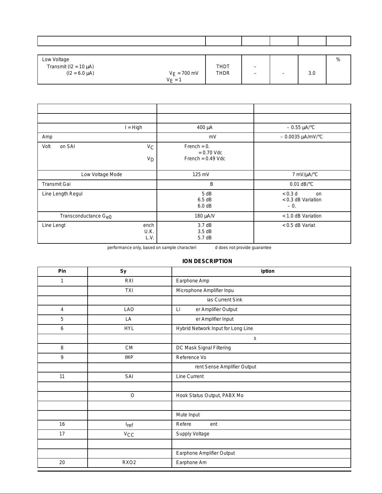
PIN FUNCTION DESCRIPTION
Pin Symbol Description
1 RXI Earphone Amplifier Input
2 TXI Microphone Amplifier Input
3 Mic Microphone Bias Current Sink
4 LAO Line Driver Amplifier Output
5 LAI Line Driver Amplifier Input
6 HYL Hybrid Network Input for Long Lines
7 HYS Hybrid Network Input for Short Lines
8 CM DC Mask Signal Filtering
9 IMP Reference Voltage
10 SAO Line Current Sense Amplifier Output
11 SAI Line Current Sense Amplifier Input
12 DCM DC Mask Select
13 HSO Hook Status Output, PABX Mode Select
14 PI Pulse Input
15 MUT Mute Input
16 I
17 V
ref
CC
18 Gnd Ground
19 RXO1 Earphone Amplifier Output
20 RXO2 Earphone Amplifier Inverted Output
Reference Current
Supply Voltage
MOTOROLA ANALOG IC DEVICE DATA
5
Page 6

TCA3388
DESCRIPTION OF THE CIRCUIT
Concept
With a TCA3388, a microcontroller and a ringer, a basic
telephone set can be built according to the concept depicted
in Figure 1.
In off–hook position, the application is in speech mode.
The line current flows through transistor T2 and supplies the
externals (microcontroller) at the supply point VCC which is
stabilized by the TCA3388. The V
adjusted by the external components Z0, Z1, Z21 and R1
which are in a regulator loop, acting on transistor T2. The ac
, I
line
characteristic is
line
Figure 1. T elephone Concept with TCA3388
impedance is generated in a similar way . The handset can be
connected directly to the TCA3388. Via a logic level interface,
the microcontroller drives the TCA3388 to perform the
DTMF/pulse–dialing. The user keyboard has to be connected
to the microcontroller. In on–hook position, a ringing melody
can be generated with a ringer application.
The block diagram of the TCA3388, in Figure 2, shows the
basic blocks of the device plus the essential external
components.
A/B
Line +
C20
Line –
Hookswitch
R6
R9
Z0Z1
Z21
Ringer
Handset
R1
Figure 2. Block Diagram of the TCA3388 with Essential Components
Z0
Z21
C5
RXO1
19
RXO2
20
RXI
TXI
Mic
Mute, AGC
1
2
3
Ear
Mute, AGC
Mic
TCA3388
Z2
C17
R19
7 8 10 5 9 16
HYS CM SAO LAI IMP I
DC Mask Generation
2–4 Wire Conversion
SAI
11
Z
DCM
R1
Z1
R20
6
HYL
AC Termination
Line Length AGC
Protection
Micro–Interface
DCM MUTPIHSO
12
13 14 15
R22
C16
Hook–Detect
PABX
To/From
Microcontroller
DTMF
T2
V
CC
Gnd
Supply–
Stabilizer
References
Line
Driver
R12
ref
MicroTCA3388
V
CC
17
Gnd
18
LAO
4
T2
C7
T3
6
MOTOROLA ANALOG IC DEVICE DATA
Page 7

TCA3388
DC CHARACTERISTICS AND ST ARTUP
The dc mask has the general form as depicted in Figure 3.
The TCA3388 offers the possibility to adjust the dc
characteristics of all 4 regions via mask selection and
hardware adjustments.
The selection of the 3 masks, France, United Kingdom
and Low Voltage, can be done via the Z
network at Pin
DCM
DCM as shown in Figure 4. For French and U.K. masks, the
region 3 with the high slope is within the normal dc feeding
conditions. For Low Voltage mask the region 3 will be outside
this and the dc mask is mainly determined by regions 1
and 2.
Figure 3. General Form of the DC Mask
of the TCA3388
V
Line
4
V
LP
3
V
LK
V
LC
2
1
Figure 4. Selection of the Country Mask via Pin DCM
I
µ
( A)
DCM
FR
14
11
LV
4
0
0.5 2.0 2.5 3.0 3.2
Z
L.V . FRU.K.
for the L.V., U.K. and FR Mask
DCM
CC
R23
56 k
R24
47 k
U.K.
C21
10
V
(V)
DCM
DCMDCMVDCM
µ
R25
1.0 M
C18
470 n
0
I
LC
Region 1: Startup, Low Line Current, High Slope
Region 2: Mid–Range Line Current, Low Slope
Region 3: High Line Current, High Slope
Region 4: Overload Protection
I
LP
Figure 5. DC Part of the Block Diagram of the TCA3388
Line +
C16
Z2
Line –
Z1
HYL
HYS
2
I
I2S
L
CM
G
G
CM
I
LKIVLP
IMP
RX
SAI
1.6 V
I
Line
2 V
BE
VO1
The capacitor in the U.K. network is to ensure a stable
selection of the mask during all working modes and
transitions. The capacitor in the French network is used to
create a startup in Low Voltage Mask.
The adjustment possibilities will be discussed below with
the aid of the block diagram of Figure 5.
T2
Z21
SAO
TCA3388
Z0
LAI
LAO
Gnd
VO2
R1
T3
R5
C7
V
CC
MOTOROLA ANALOG IC DEVICE DATA
7
Page 8

TCA3388
The TCA3388 offers the possibility to connect 2 sidetone
networks Z1 and Z2. For correct dc operation, the dc
impedance of these networks must be equal. When only 1
sidetone network is used, Pin HYS has to be connected to
HYL. All formulas below are based on a single sidetone
network, so only Z1 appears. When 2 sidetone networks are
used, Z1 has to be replaced by Z1//Z2.
In region 1, the transfer of the amplifier G at the HYL/HYS
inputs equals zero. The voltage difference between SAO and
SAI will equal VO1. The slope RE1 of the V
characteristic will equal:
Z0
RE1+
In region 2, the output current of the amplifier G will be
proportional to the input current. As a result the voltage
between SAO and SAI will increase with the line voltage.
Speech signals on the line are of no influence on this
because they are filtered out via capacitor C16. The slope
RE2 of the V
, I
Line
RE2+
Line
R1 x
ǒ
R1 x
1
characteristic will equal:
ȡ
1
)
ȧ
Ȣ
In region 3, the output current of the amplifier G is kept
constant. As a result the slope in region 3 will equal the slope
of region 1.
The transfer from region 2 to 3 occurs at the point VLK, I
defined by:
)
RI
Z1
Z21
1
)
Ǔ
Z21
Z0
ȣ
ȧ
Ȥ
Line
, I
Line
LK
When the line voltage becomes lower than VLP, the
overload condition is removed and the TCA3388 will leave
region 4.
The current drawn from the line by the dc part is used to
supply the TCA3388 and peripheral circuits. The excess loop
current is absorbed by the voltage regulator at Pin VCC,
where a filter capacitor is connected. The reference for the
circuit is Pin Gnd.
Startup of the application is ensured by an internal startup
circuit. When the line current flows, the hook status output
pin HSO goes high. This informs the microcontroller that the
set is off–hook. When the line current is no longer present the
pin will go low again. Because the line current is monitored,
and not the line voltage, also an interrupt of the exchange
can be recognized.
AC CHARACTERISTICS
Impedance
In Figure 6, the block diagram of the TCA3388 performing
the ac impedance is depicted. As can be seen it is partly
common with the dc mask block diagram. The part
generating the dc mask is replaced by a dc voltage source
because for ac, this part has no influence.
Figure 6. AC Stage of the TCA3388
Line +
Z0
T2
R5
VLK = Z1 x I2CD + 2 VBE + VCD + VO2
Z21
xǒZ1 x I2CD)2V
Z0
ILK+
I2CD
With:
and 2 VBE 1.4 V, V02 1.1 V
When the French or U.K. mask is selected, this transfer
takes places for line currents of 30 mA to 40 mA depending
on the components settings. With the Startup and Low
Voltage mask, the transfer lies outside the normal operating
range with line currents of 90 mA or more. In most
applications the transfer from region 1 to 2 takes place for line
currents below 10 mA.
With proper settings, region 4 is entered only during an
overload condition. In this mode, the power consumption in
the telephone set is limited. In order to detect an overload
condition, the voltage between the Pins LAI and SAO is
monitored. When the voltage difference is larger than the
threshold V
for the line voltage VLP at this point is given as:
VLP+
When the protection mode is entered, the line current is
reduced to a lower value ILP of:
ILP+
I2C)I2D
+
Clamp1
Z0
Z21
V
2
, the protection is made active. The relation
xV
Clamp2
R1
,andVCD+
Clamp1
)(VO1 – VO2
)
R1
BE
VCD)
)
Ǔ
)
VC)
V
VO2
2
CD
V
D
,
V
TCA3388
LAI
Z21
SAO
V02
VO1
SAI
Line –
When calculating the ac loop, it can be derived that the set
impedance Zin equals
V
Zin+
As can be noticed, the formula for the ac impedance Z
equals the formula for the dc slope in regions 1 and 3.
However, because for the dc slope the resistive part of Z0
and Z21 are used, the actual values for Zin and the dc slopes
do not have to be equal.
A complex impedance can be made by making either Z0
or Z21 complex. When Z0 is made complex to fit the set
impedance the transmit characteristics will be complex as
well. The complex impedance is therefore preferably made
via the Z21 network. Because Z21 is in the denominator of
the Zin formula, Z21 will not be a direct copy of the required
impedance but a derivative of it. Figure 7 gives this derived
network to be used for Z21.
Line
I
Line
+
R1ǒ1
R1
)
LAO
Gnd
Z0
Z21
T3
Ǔ
[
R1 x
CC
C7
Z0
Z21
in
8
MOTOROLA ANALOG IC DEVICE DATA
Page 9

TCA3388
Figure 7. Derived Network for Z21 in Case of
Complex Set Impedance
Gnd
Ǔ
R
v
R
w
C
w
Ǔ
Ǔ
R
R1xZ0
Rb–R1
ǒ
Ra)
b
2
xC
v
Rb–R1
b
SAO LAI
R
a
R
b
C
b
Rv+
Rw+
ǒ
2
Ra)
R1xZ0ǒRa–R1
4R
4R
Cw+
b
R1 x Z0
TRANSMIT
When a current is injected on Pin LAI, via the loop
depicted in Figure 6, a signal is created on the line. In this
way the microphone signals and DTMF signals (from an
external source) are transmitted. It can be derived that the
signal voltage on the line (V
current injected in LAI (I
V
Line
+
LAI
–I
LAI
With this relation, a simplified replacement circuit can be
made for the transmit amplifier (see Figure 8). Here the
product of I
and Z0 is replaced by one voltage source.
LAI
Figure 8. Replacement Diagram for
the Transmit Amplifier
–I
*Z0
LAI
) depends on the signal
Line
) according to:
Z0 x Z
V
Line
Line
Z
Line
Z
Line
Z
in
x
Zin)
The microphone signal current is derived from the
microphone signal according to the schematic in Figure 9.
Figure 9. Microphone Amplifier Input Stage
Ku
TCA3388
Line AGC
Mute
I
LAI
R
C
Mic
Handset
Microphone
Mic
V
CC
C
u
R
u
TXI
Mic
I
u
R
TXI
The input stage of Figure 9 consists of a current amplifier
with transfer Ku, an input impedance of 1.0 k (R
TXI)
, plus an
attenuator which reduces the signal current at high line
currents (AGC). This attenuator can be switched on/off via
the microcontroller. The input current Iu within the telephony
speech band is derived from the microphone signal according
V
Iu+
R
Mic
)
u
Ru)
R
TXI
With: Vu = signal of the microphone only loaded with R
[
V
u
R
u
Mic
The overall gain from microphone to line (ATX) now follows
as
ATX+
V
Line
V
u
+
Ku
R
Z0 x Z
x
Zin)
u
Line
Z
Line
Practically, the gain can be varied only with Z0, Ru and
R
.
Mic
The TCA3388 offers the possibility to mute the
microphone, also called privacy mode, by making the MUT
Pin high. During pulse–dialing, the microphone bias is
switched off. Pin Mic will be made high impedance, shutting
off the microphone dc current. This reduces the current
consumption of the circuit during pulse–dialing.
MOTOROLA ANALOG IC DEVICE DATA
9
Page 10

Line +
TCA3388
Figure 10. Receive Part of the TCA3388
R20Z1
C17
R19Z2
+ V01
BE
HYL
G
G
e
e
Line Mute
AGC
R1
IMP
HYS
2V
SAI Gnd
Line –
RECEIVE
The receive part of the TCA3388 is shown in Figure 10.
The receive signal is picked up by the amplifiers at the
HYL/HYS inputs. These are the same amplifiers present in
the dc loop of Figure 5. The signal is first converted to current
by the transconductance amplifier with transfer Ge. The
multiplier placed after performs the line length AGC. It
switches over between the 2 signals at HYS and HYL
according to the line current via a modulation factor m.
Afterwards, the current is converted back to voltage via the
external feedback network Z
available at output RXO1, and inverted at RXO2.
From the diagram of Figure 10 the receive gain (ARX) can
be derived as:
V
ARX+
RXO
V
Line
+
Ge x R1 x Z
. The resulting voltage is
Load
1
ǒ
x
Load
Z
H
)
1
Ǔ
Z
in
1.6 V
V
ref
TCA3388
RXO1
RXI
R
Load
–1X
C
Load
RXO2
C
ear
Handset
Earpiece
SIDETONE
When a transmit signal is transmitted to the line, a part of
the signal is returned to the receive channel due to the
architecture of the 2 to 4 wire conversion of the hybrid. During
transmit, the signal on the line will be –I
receive, the signal on the line will be I
replacing Zin in the formula for the receive gain, it follows that
the signal on the earpiece output due to a sending signal on
the line will be:
V
ear
V
Line (transmit)
In applications with 1 sidetone network where HYS is
connected to HYL, it follows:
+
GexR1xZ
H
+
R1 x Z1
R20
1
Z
Load
+
Z
Line
1
HL
Line
ǒ
x
x Z
Line
x Zin. When
1
–
Z
H
. During
1
Ǔ
Z
Line
H
H
+
R1 x Z1
+
mx
R20
R1 x Z1
in case of 1 sidetone network and
R20
)
(m –1)
R19
R1 x Z2
in case of
1
With:
Z
HYS connected to HYL, or
1
Z
2 sidetone networks
More information on ZH and the modulation factor m can
be found under the sidetone characteristics.
The earpiece can either be connected as a single ended or
as a differential load. The above calculated gain is valid for the
single ended case. When connecting as a differential load, the
gain is increased by 6.0 dB. The TCA3388 offers the
possibility to mute the signal coming from the line to the
earpiece. This can be useful during pulse– and DTMF–dialing.
10
ZH has to be chosen according the average line
impedance, and the average linelength of the countries
involved in the application. A complex sidetone network can
be made via a complex Z1 which is preferred above making
R20 complex. The coupling capacitor C17 in series with R20
is meant only to block dc.
For applications with 2 sidetone networks it follows:
1
Z
H
The ZH thus exists as ZHL for long lines with low line
currents and as ZHS for short lines with high line currents.
This can be useful in applications such as DECT and
handsfree where the sidetone has to be minimized to reduce
the effect of delayed echoing and howling respectively. The
TCA3388 will automatically switch over between the 2 hybrid
networks as a function of line current. This is expressed in the
R20
+
m
R1 x Z1
m
MOTOROLA ANALOG IC DEVICE DATA
)
(m –1)
1
)
Z
(m – 1)
HL
R19
R1 x Z2
1
Z
HS
+
Page 11

TCA3388
factor m. The relation between the line current and the factor
m is depicted in Figure 1 1.
Figure 11. Modulation Factor m as a Function
of Line Current
m
1.0
0.5
I
III0
For low line currents below I
LstopLmLstart
, thus long lines, the
Lstart
Line
factor m equals 1. This means the hybrid network ZHL is fully
used. For high line currents above I
, thus short lines, the
Lstop
factor m equals 0. This means the hybrid network ZHS is fully
used. Both networks are used 50% for the intermediate line
current Ilm.
The switch over between the 2 networks takes place in
region 3 for the French and U.K. mask and in region 2 for the
Low Voltage mask.
LINE LENGTH AGC
The TCA3388 offers the possibility to vary the transmit and
receive gain over line length in order to compensate for the
loss in gain at longer line lengths. In the block diagrams of the
transmit and receive channels (Figures 9, 10) the line AGC is
drawn. The line AGC can be switched off by connecting a
150 kΩ resistor between HSO and Gnd. In this case, the
transmit and receive gain are lowered by 2.0 dB with respect
to the value calculated in the formulas above.
The line AGC characteristics for both transmit and receive
channel have the general shape depicted in Figure 12.
Figure 12. General Line AGC Characteristics
Gain
Gain
Nominal
Gain
Reduced
Gain
I
Lstart
I
Lrange
For low line currents, and thus long lines, the gains are
nominal. When the line current has increased above I
Nominal Gain
+
1
)
IL–I
I
Lrange
Lstart
I
Line
Lstart
with a current I
, the gain is reduced by 6.0 dB. Due to
Lrange
the general characteristics of the line AGC curve, the gain will
be decreased further for higher currents.
For France and U.K., the line AGC will be active in region
3 of the dc characteristics. The I
is approximately equal
Lstart
to the ILK. The range is calculated from:
I
Lrange
Z1 x(I2R – I2CD
+
R
E3
)
For Low Voltage mask, the line AGC is active in region 2.
DIALING
Pulse–dialing is performed by making pin PI high. As a
result the output LAO goes low and the loop will be
disconnected. Internally the current consumption of the
circuit is reduced and the current through the microphone is
switched off.
DTMF–dialing is performed by supplying a DTMF signal
current to Pin LAI. This is the same node where the
microphone signal currents are internally applied. Therefore,
for the DTMF gain the same formulas apply. Because the
microphone preamplifier is bypassed, there is no influence
on DTMF signals by the line length AGC.
A DTMF confidence tone can be generated on the
earpiece by injecting a signal current at the RXI pin. Because
only the earpiece amplifier itself is used, there are no effects
from AGC or hybrid switchover.
For correct DTMF–dialing the pin MUT has to be made
high. This mutes both the microphone and earphone
preamplifier. In this way signals from the microphone will not
be amplified to the line and signals from the line are not
amplified to the earpiece.
The complete interfacing of the DTMF generator with the
TCA3388 is shown in the typical application.
SUPPORT MATERIAL
Device Specification: Brief description of the TCA3388,
block diagram, device data, test
diagram, typical application
User manual TCA3388:Extended description of the circuit
and its concept, adjustment
procedure, application hints and
proposals
Demonstration board: Shows performance of the TCA3388
in its basic application
TYPICAL APPLICATION
The typical application below is based on the demoboard
of the TCA3388. It contains the speech transmission part,
diode bridge, hook switch and microcontroller interfacing.
The dc mask setting on the bottom left is given for France,
U.K. and Low Voltage applications. The component values
are given in the table of Figure 14. The line driver is extended
with T1, D5 and R3 which increases the signal swing under
low line voltage conditions.
MOTOROLA ANALOG IC DEVICE DATA
11
Page 12

TCA3388
Rp
T2
Line +
Ring
A/B
On–Hook
D1 D2
R3
R5
Z1
C1
Off–Hook
T1
D5
D4D3
T3
B/A
C2
R1
Line–
Line Driver
Mic
V
R7
C6
R9
Mic +
Mic –
Ear +
Ear –
R6
R27
Gnd
C3
Receive GainPABX
C20
Figure 13. T ypical Application
C13
R14
C10
C11
R15
R18
C12
R28 R21
R13
C23
Z1
R16
R17
Z2
Z0
Z21
Long Line
Short Line
C16
R29
C14
R20
C15
R19
C24
C25
C17
C5
1
20
TCA3387
TCA3388
TCA3389
10
11
C8R11
C4
R8
Gain
Sidetone Balance
DTMF
Transmit Gain
R26
FR LV UK
R23
C7
C22
C19
C26
R12
R22
R24
C21
C18
R25
Mask Setting
12
DTMF
HSO
Pulse
Mute
V
CC
Gnd
MOTOROLA ANALOG IC DEVICE DATA
Page 13

TCA3388
Item
R
Figure 14. List of Components for T ypical Application TCA3388
Location
on Board
R1 Line Driver 16 16 18
R3 Line Driver 10 k
R5 Line Driver 1.0 k
R6 Receive Gain 150 k
R7 Transmit Gain 2.2 k
R8 DTMF Gain 470 k
R9 Transmit Gain 39 k
R11 DTMF Gain 56 k
R12 I
R13 Z0 580 k 560 k 330 k
R14 Z0 – 680 k 620 k
R15 Z1 620 k 1.2 m 1.8 m
R16 Z1 130 k 300 k 330 k
R17 Z2 – 620 k 820 k
R18 Z2 – 820 k 1.5 m
R19 Sidetone Bal – 18 k 39 k
R20 Sidetone Bal 7.5 k 15 k 22 k
R21 Z21 16 k 16 k 18 k
R22 PABX 150 k
R23 Mask Setting – – 56 k
R24 Mask Setting – – 47 k
R25 Mask Setting – 1.0 m –
R26 Pin 19 10 Stability
R27 Pin 20 10 Stability
R28 Z21 0
R29 Transmit Gain 1.0 k V
Rp Line+ 0 22 22
C1 A/B 10 n EMC
C2 Line Driver 470 p
C3 Receive Gain 220 p
C4 DTMF Gain 10 n
C5 Transmit Gain 10 n
C6 Transmit Gain 6.8 n
C7 Pin 17 220 µ VCC, 10 V
C8 DTMF Gain 10 n
C10 Z0 – 4.7 n 330 p
C11 Z1 220 p 120 p 150 p
C12 Z2 – 82 p 150 p
C13 Z21 470 p
C14 Sidetone Bal 470 p Stability
C15 Sidetone Bal – 470 p 470 p Stability
C16 Pin 8 680 n 680 n 2.2 µ DC Mask
C17 Sidetone Bal 680 n
, Pin 16 121 k 1.0%
ref
Basic L.V . France U.K.
Application
Mic
emarks
MOTOROLA ANALOG IC DEVICE DATA
13
Page 14

TCA3388
Figure 14. List of Components for T ypical Application TCA3388
Location
Item
Item
C18 Mask Setting – 470 n –
C19 Pin 19 100 n Stability
C20 Pin 20 100 n Stability
C21 Mask Setting – – 10 µ 10 V
C22 Pin 17 100 n Close to Pin
C23 Z21 –
C24 Transmit Gain 10 µ V
C25 Pin 2 4.7 n EMC
C26 Pin 16 1.0 n EMC
T1 Line Driver MPSA92 PNP–HV
T2 Line Driver MJE350 PNP–HV
T3 Line Driver MPSA42 NPN–HV
D1–D4 Bridge 4 x 1N4004 HV
D5 Line Driver 1N4004 Signal
Z1 A/B MKP1V270 Sidac
Location
on Board
on Board
Application
U.K.FranceBasic L.V .
, 10 V
Mic
Remarks
Remarks
14
MOTOROLA ANALOG IC DEVICE DATA
Page 15

TCA3388
OUTLINE DIMENSIONS
DP SUFFIX
PLASTIC PACKAGE
CASE 738-03
ISSUE E
-T-
SEATING
PLANE
-A-
1120
B
110
C
K
E
N
GF
D
20 PL
0.25 (0.010) T A
M M
PLASTIC PACKAGE
CASE 751D–03
–A–
20
11
–B–
P10X
0.010 (0.25)
1
10
D20X
S
M
0.010 (0.25) B
A
T
S
C
SEATING
–T–
18X
G
K
PLANE
FP SUFFIX
ISSUE E
M
M
B
J
F
L
J 20 PL
0.25 (0.010) T B
M
M
M M
R
X 45
NOTES:
1. DIMENSIONING AND TOLERANCING PER ANSI
Y14.5M, 1982.
2. CONTROLLING DIMENSION: INCH.
3. DIMENSION L TO CENTER OF LEAD WHEN
FORMED PARALLEL.
4. DIMENSION B DOES NOT INCLUDE MOLD
FLASH.
INCHES MILLIMETERS
MIN MINMAX MAX
DIM
A
B
C
D
E
F
G
J
K
L
M
N
NOTES:
1. DIMENSIONING AND TOLERANCING PER
ANSI Y14.5M, 1982.
2. CONTROLLING DIMENSION: MILLIMETER.
3. DIMENSIONS A AND B DO NOT INCLUDE
MOLD PROTRUSION.
4. MAXIMUM MOLD PROTRUSION 0.150
(0.006) PER SIDE.
5. DIMENSION D DOES NOT INCLUDE
DAMBAR PROTRUSION. ALLOWABLE
DAMBAR PROTRUSION SHALL BE 0.13
(0.005) TOTAL IN EXCESS OF D DIMENSION
AT MAXIMUM MATERIAL CONDITION.
DIM MIN MAX MIN MAX
A 12.65 12.95 0.499 0.510
B 7.40 7.60 0.292 0.299
C 2.35 2.65 0.093 0.104
D 0.35 0.49 0.014 0.019
F 0.50 0.90 0.020 0.035
G 1.27 BSC 0.050 BSC
_
J 0.25 0.32 0.010 0.012
K 0.10 0.25 0.004 0.009
M 0 7 0 7
P 10.05 10.55 0.395 0.415
R 0.25 0.75 0.010 0.029
1.070
1.010
0.260
0.240
0.180
0.150
0.022
0.015
0.050 BSC
0.070
0.050
0.100 BSC
0.015
0.008
0.140
0.110
0.300 BSC
°
15
0
0.040
0.020
__
25.66
6.10
3.81
0.39
1.27
0.21
2.80
°
0.51
27.17
6.60
4.57
0.55
1.27 BSC
1.77
2.54 BSC
0.38
3.55
7.62 BSC
°
°
0
15
1.01
INCHESMILLIMETERS
__
MOTOROLA ANALOG IC DEVICE DATA
15
Page 16

TCA3388
Motorola reserves the right to make changes without further notice to any products herein. Motorola makes no warranty , representation or guarantee regarding
the suitability of its products for any particular purpose, nor does Motorola assume any liability arising out of the application or use of any product or circuit,
and specifically disclaims any and all liability, including without limitation consequential or incidental damages. “T ypical” parameters can and do vary in different
applications. All operating parameters, including “T ypicals” must be validated for each customer application by customer’s technical experts. Motorola does
not convey any license under its patent rights nor the rights of others. Motorola products are not designed, intended, or authorized for use as components in
systems intended for surgical implant into the body, or other applications intended to support or sustain life, or for any other application in which the failure of
the Motorola product could create a situation where personal injury or death may occur. Should Buyer purchase or use Motorola products for any such
unintended or unauthorized application, Buyer shall indemnify and hold Motorola and its officers, employees, subsidiaries, affiliates, and distributors harmless
against all claims, costs, damages, and expenses, and reasonable attorney fees arising out of, directly or indirectly, any claim of personal injury or death
associated with such unintended or unauthorized use, even if such claim alleges that Motorola was negligent regarding the design or manufacture of the part.
Motorola and are registered trademarks of Motorola, Inc. Motorola, Inc. is an Equal Opportunity/Affirmative Action Employer.
How to reach us:
USA/ EUROPE: Motorola Literature Distribution; JAPAN: Nippon Motorola Ltd.; Tatsumi–SPD–JLDC, Toshikatsu Otsuki,
P.O. Box 20912; Phoenix, Arizona 85036. 1–800–441–2447 6F Seibu–Butsuryu–Center, 3–14–2 Tatsumi Koto–Ku, Tokyo 135, Japan. 03–3521–8315
MFAX: RMF AX0@email.sps.mot.com – T OUCHTONE (602) 244–6609 HONG KONG: Motorola Semiconductors H.K. Ltd.; 8B Tai Ping Industrial Park,
INTERNET: http://Design–NET.com 51 Ting Kok R oad, Tai Po, N.T., Hong Kong. 852–26629298
16
◊
MOTOROLA ANALOG IC DEVICE DATA
TCA3388/D
*TCA3388/D*
 Loading...