

Page 1

TC5299J
TC5299J
FAST ETHERNET PCMCIA
LAN CONTROLLER
4FL No. 106 Hsin-Tai Wu Road,
Sec. 1, Hsichih,
Taipei Hsien, Taiwan R.O.C.
TEL: 886-2-2696-1669
FAX: 886-2-2696-2220
http:\\www.tmi.com.tw
-1-
Ver. 0.1
07/04/01
Page 2

TC5299J
TABLE OF CONTENTS
1 Introduction .................................................................................................................................3
1.1 General Description.............................................................................................................................................3
1.2 Features...............................................................................................................................................................3
2 Block Diagram .............................................................................................................................3
3 Pin Description.............................................................................................................................4
3.1 Pin Out Diagram .................................................................................................................................................4
3.2 Signal Description...............................................................................................................................................5
3.3 Power On Configuration.....................................................................................................................................8
4 I/O and Mapping .......................................................................................................................10
4.1 I/O Port Address Mapping................................................................................................................................10
4.2 EEPROM/SRAM Memory Mapping................................................................................................................10
4.3 Attribute Memory Mapping..............................................................................................................................11
4.3.1 Attribute Memory Map......................................................................................................................11
5 Configuration Registers ............................................................................................................13
5.1 Configuration Register A..................................................................................................................................13
5.2 Configuration Register B ..................................................................................................................................13
5.3 Configuration Register C ..................................................................................................................................14
5.4 Hardware Configuration....................................................................................................................................14
5.5 MII/PHY Control Register................................................................................................................................15
5.6 TC5299J Core Registers Assignment................................................................................................................15
5.7 Register Descriptions........................................................................................................................................18
5.7.1 Command Register (CR) 00H (Read/Write)......................................................................................18
5.7.2 Data Configure register (DCR) 0EH(Write)....................................................................................19
5.7.3 Transmit configuration Register (TCR) 0DH(Write) ........................................................................19
5.7.4 Transmit Status Register (TSR) 04H(Read).....................................................................................20
5.7.5 Receive Configuration Register (RCR) 0CH(Write)........................................................................21
5.7.6 Receive Status Register (RSR) 0CH(Read)......................................................................................21
5.7.7 Interrupt Mask Register (IMR) 0FH(Write)....................................................................................22
5.7.8 Interrupt Status Register (ISR) 07H(Read/Write)............................................................................23
5.8 Network Tally Counter Registers (CNTR)........................................................................................................23
5.9 Number of Collisions Register (NCR)..............................................................................................................24
5.10 Physical Address Register (PAR0-PAR5).........................................................................................................24
5.11 Multicast Address Registers (MAR0-MAR7)...................................................................................................24
5.12 DMA Registers..................................................................................................................................................25
5.13 LOCAL DMA RECEIVE REGISTERS...........................................................................................................25
5.14 REMOTE DMA REGISTERS..........................................................................................................................25
5.15 (i) Local DMA Transmit Registers ............................................................................................... ....................25
5.16 (ii) Local DMA Receive Registers....................................................................................................................26
5.17 (iii) Remote DMA registers...............................................................................................................................26
6 Electrical Specification and Timing.........................................................................................28
7 Physical Dimension....................................................................................................................31
Notice.................................................................................................................................................32
-2-
Ver. 0.1
07/04/01
Page 3
Fast Ethernet PCMCIA Controller
1 Introduction
1.1 General Description
The TC5299J is a 10/100 PCMCIA Ethernet controller, include a standard MII interface. It provides an 8/16-bit
PCMCIA interface to host CPU and buffer memory into single chip to minimize the chip gate count.
The TC5299J supports both half-duplex and full-duplex (both 10BT or 100BTX) operation environment.
1.2 Features
!"PCMCIA 2.01 bus interface.
!"Use serial EEPROM 93C56/66 to store CIS.
!"Internal 5V to 3.3V regulator.
Ethernet LAN features:
!"Integrated Fast Ethernet MAC and SRAM in one chip.
!"Supports both 10Mbps and 100Mbps operation.
!"IEEE 802.3/802.3u compatible.
!"Full-duplex or half-duplex operation supported for both 10Mbps and 100Mbps operation.
!"NE2000 register definitions.
!"Supports 3.3V or 5V signaling environment.
!"The size of built-in Buffer RAM is 8k x 16 bits. It does not need the extra SRAM in the application circuit.
!"Supports loop-back mode for self-testing.
!"Supports 256/512 bytes EEPROM interface.
!"LED interface supported.
!"Supports MII bus interface.
!"Flow control ability
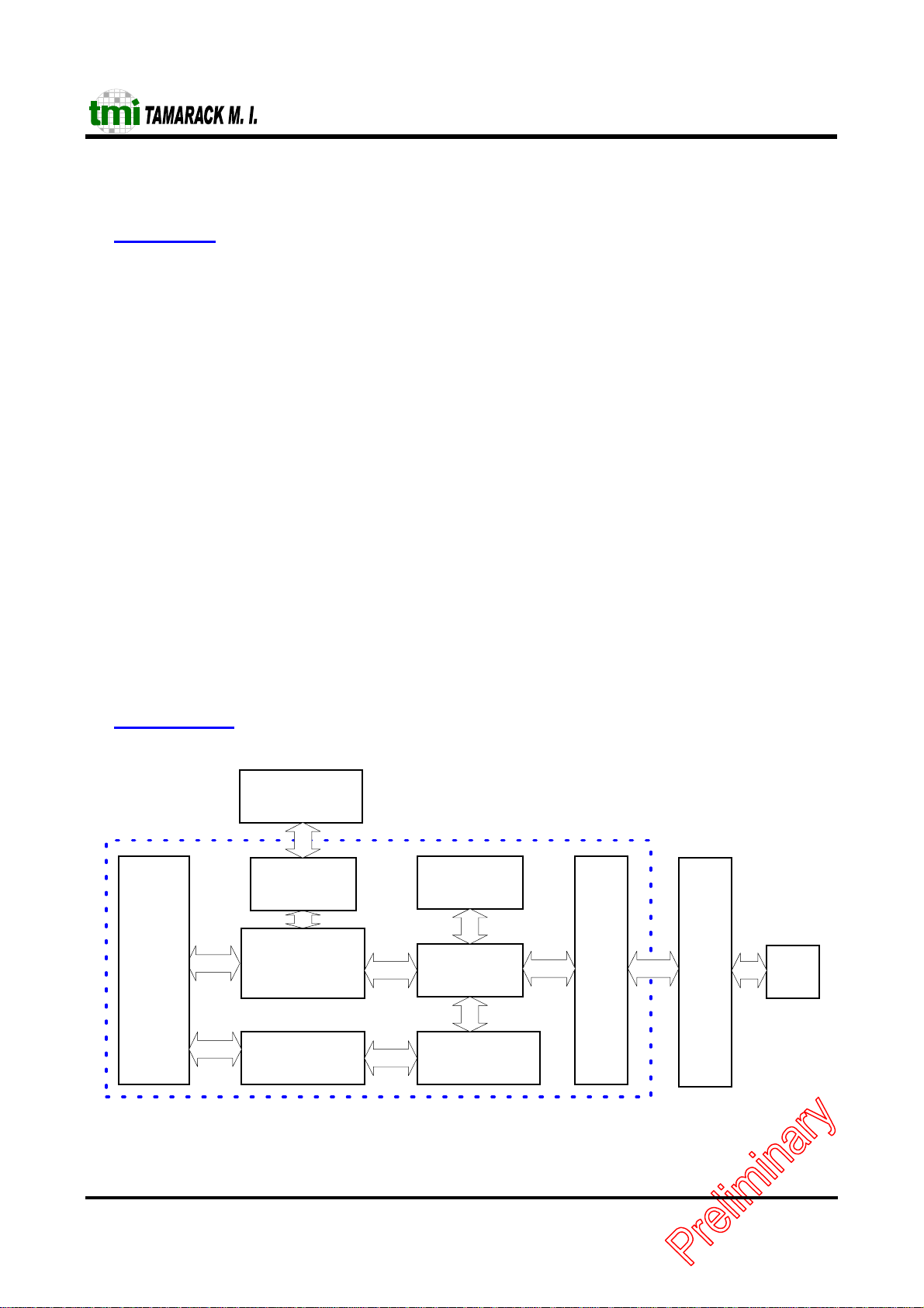
2 Block Diagram
TC5299J
PCMCIA
Inte r fa c e
EEPROM
EEPROM
Control Circuit
PCMCIA
Command
Decoder
DMA Buffer
Control Logic
SRAM
FIFOs
FIFO
Controller
-3-
MAC
PHY
TW R
RJ45
Ver. 0.1
07/04/01
Page 4

3 Pin Description
3.1 Pin Out Diagram
TC5299J
NC
NC
GNDAT
VCCAT
VCC5A
VCC5R
NC
VCC3IO
RSTN
GND3IO
JMP0
GND3D
GND3IO
JMP1
NC
VCC3D
VCC3IO
SD15
SD14
SD13
SD12
GND3IO
SD11
SD10
VCC3D
SD9
SD8
VCC3IO
INT
IOR
OE
GND3IO
G
N
V
V
C
C
C
C
5
A
N
N
C
R
C
234567891011121314151617181920212223242526272829303132
97
98
99
100
101
102
103
104
105
106
107
108
109
110
111
112
113
114
115
116
117
118
119
120
121
122
123
124
125
126
127
128
A
1
G
G
D
N
N
A
D
D
1
A
A
0
P
R
128pin LQFP
V
G
C
V
N
D
D
P
V
C
C
C
A
C
C
1
D
A
N
0
P
C
P
C
V
G
C
N
C
3
IONCNCN
G
D
N
3
D
ION
3
C
D
G
N
M
D
D
3
I
NCN
C
D
O
TC5299J
V
L
C
E
E
C
L
E
D
C
L
S
A
L
3
E
E
I
D
D
O
S
F
G
N
D
3
I
O
G
N
D
3
IOX1X
2
6566676869707172737475767778798081828384858687888990919293949596
64
63
62
61
60
59
58
57
56
55
54
53
52
51
50
49
48
47
46
45
44
43
42
41
40
39
38
37
36
35
34
33
VCC3D
VCC5A
VCC5R
VCC5A
VCC3IO
MDC
RXD3
RXD2
GND3IO
RXD1
RXD0
X25M
RXDV
RXC
RXER
GND3IO
TXC
TXEN
TXD0
TXD1
GND3IO
TXD2
TXD3
GND3D
COL
CRS
VCC3IO
EXLEDF
EXLEDL
CE1
WE
NC
S
S
S
S
S
S
S
S
S
S
S
S
S
S
I
S
S
S
V
O
A
C
W
9
C
3
I
O
G
A
A
A
A
N
8
7
D
3
D
A
6
5
4
S
A
A
A
3
2
1
NCR
G
A
N
0
D
3
I
O
I
W
E
N
S
A
G
P
T
I
A
T
C
K
D
O
N
0
I
D
S
3
1
I
6
O
I
R
G
V
D
D
C
1
2
C
3
I
O
V
D
3
D
D
C
5
4
C
3
D
G
D
D
N
6
7
D
3
I
O
-4-
Ver. 0.1
07/04/01
Page 5

3.2 Signal Description
PCMCIA Bus Interf ace Pins
Symbol Pin # I/O Description
SA[9:0] 3-5
7-12,
14
SD[15:8]
SD[7:0]
RST 16 I/O RST is active high and places the TC5299J in a reset mode
RSTZ 105 O RSTZ is an active low signal. It is an inverted signal of RST.
WAIT* 17 O This pin is set low to insert wait states during Remote DMA
REG* 19 I REG is an active low input used to determine whether a host
IOR* 126 I Read Strobe: Strobe from host to read registers or Remote DMA
IOW* 2 I Write Strobe: Strobe from host to read registers or Remote DMA
OE* 127 I Host memory read strobe, when OE* and REG* both low the
WE* 34 I Host memory write strobe, After Power reset if TC5299J is
INPACK* 18 O An active low signal. Asserted if the host access register or
IO16* 21 O IO16* is driven by TC5299J to support host 16 bits access cycle.
INT*
(RDY/BSY*)
CE1* 35 I Card enable 1, is active low signals driven by the host. This
114-117,
119-120,
122-123,
31-29,
27-26,
24-22
125 O While the TC5299J is configured as a memory device, this pin
I The address signal lines of PCMCIA Bus are used to select a
register to be read or written and attribute memory enabled.
I/O Register Access, with DMA inactive, SD0-SD7 are used to
read/write register data. SD8-SD15 invalid during this state.
Remote DMA Bus Cycle, SD0-SD15 contain packet data.
Direction of transfer depends on Remote read/write.
immediately. During falling edge the TC5299J controller loads
the configuration from JMP0 – JMP8.
transfer.
access is to Attribute memory or to common memory. If REG is
low the access is to attribute memory, if REG* is high the access
is to common memory. REG* is also asserted low for all accesses
to the TC5299J IO Registers.
read.
write.
attribute memory can be read. When OE* is low and REG* is
high common memory can be read .
configured to memory write enable, then WE and REG* is both
low, Attribute memory can be written. When WE is low and
REG* is high common memory can be written.
Remote DMA read cycle.
servers as RDY/BSY* pin, If the TC5299J is ready to perform a
transfer, this pin is set high. When TC5299J is operated at I/O
mode, this pin is used as an interrupt pin. It indicates that the
TC5299J needs host service. RDY/BSY* state can be read from
the pin Replacement Register (CCR2). While LAN and MODEM
both functions are enabled and IntSel bit in control Register
(CCR5) is zero. This pin output is logical OR of LAN and
MODEM interrupt.
signal provides a card select based on the address decode (decode
by the host).
TC5299J
-5-
Ver. 0.1
07/04/01
Page 6

EEPROM/LED Inter fa ce Pins
Symbol Pin # I/O Description
EECS 73 O EEPROM chip select. It is asserted when to access EEPROM.
EESK/LED LA 72 O Link (on/off) & Re ce i ve d a ta ( B link) LE D p i n. I t i s al so use d as a
serial clock for EEPROM data loading.
DO/LEDS 70 I/O Speed (100M:ON/10M:OFF) & transmit data (Blink) LED pin. It
is also used as a signal for EEPROM data loading.
DI/LEDF 69 O Full-duplex (ON/OFF, Full/Half-duplex) & Collision (Blink)
LED pin. It is a data output pin for EEPROM writing.
External PHY / MII Interface Pins
Symbol Pin # I/O Description
TXD[3:0] 42-43,
45-46
TXEN 47 I/O This pin function as transmit enable. It indicates that a
TXC 48 I Supports the transmit clock supplied by the external PMD device.
RXD[3:0] 58-57,
55-54
RXC 51 I Supports receive clock from PHY. And is recovered by the PHY.
RXDV 52 I Data valid is asserted by an external PHY when receive data is
RXER 50 I Data valid is asserted by an external PHY when receive data is
COL 40 I This pin functions as the collision detect. When the external
CRS 39 I In MII mode this pin functions as the carrier sense and is asserted
MDC 59 O MII management data clock is sourced by the TC5299J to the
MDIO 74 I/O MII management data input/output transfers contro l information
EXLEDL 36 I Low active; presents the external PHY link status.
EXLEDF 3 7 I Present the half/full duplex mode for external PHY.
Clock Interface Pins
Symbol Pin # I/O Description
X1 66 I CRYSTAL OR EXTERNAL OSCILLATOR INPUT: 50 MHz
X2 67 O CRYSTAL FEEDBACK OUTPUT: used in crystal connection
X25M 53 O 25MHz clock output
O Four parallel transmit data lines. This data is synchronized to the
assertion of the TXC signal and is latched by the e xternal PHY
on the rising edge of the TXC signal.
transmission is active on the MII port to an external PHY device.
Pull down this pin on power-on reset to select 50MHz-clock
input from pin X1. Otherwise, use 25MHz-clock input.
This clock should always be active.
I Four parallel receive data lines. This data is driven by an external
PHY that attached the media and should be synchronized with
the RXC signal.
present on the RXD[3:0] lines and is deasserted at the end of the
packet. This signal should be synchronized with the RXC signal.
present on the RXD[3:0] lines and is deasserted at the end of the
packet. This signal should be synchronized with the RXC signal.
physical layer protocol (PHY) device detects a collision, it asserts
this pin.
by the PHY when the media is active.
external PHY devices as a timing reference for the transfer of
information on the MDIO signal.
and status between the external PHY and the TC5299J.
only.
TC5299J
-6-
Ver. 0.1
07/04/01
Page 7

Power Supply Pins
Symbol Pin # I/O Description
VCCAR
GNDAR
VCCA10
GNDA10
VCCAP
GNDAP
VCCDP
GNDDP
VCCAT
GNDAT
VCC5A 101, 96, 63, 61 PWR 5V power input pin.
VCC5R 102, 62 PWR 5V power reference pin.
VCC3D,
GND3D
VCC3IO
GND3IO
JUMPER Interface Pins
Symbol Pin # I/O Description
JMP0 107 I When power on setting, this bit directly locked to CCR0, bit5.
JMP1 110 I Power on setting:
No Connection Pins
95
92
87
91
86
90
85
89
100
99
121, 112, 28, 64
6, 41, 75, 78,
108
1, 25, 38, 60,
71, 81, 104,
113, 124
13, 20, 32, 44,
49, 56, 65, 68,
79, 106, 118,
128
PWR
GND
PWR,
GND
PWR,
GND
PWR,
GND
Power input for internal circuit.
Power input for internal circuit.
3.3V power input pin, for digital core circuit.
3.3V power input pin, for I/O PAD.
0: enable I/O. For embedded system use to enable I/O mode.
1: disable I/O. For PCMCIA system use only.
Default setting is leaving this pin open.
0: separate address decode. Decode range from A0 to A5.
1: full address decode. Decode range from A0 to A9.
TC5299J
Symbol Pin # I/O Description
NC 15, 103, 111, 33 No Connection
NC 97, 98, 93, 94,
83, 77, 84, 82,
80, 76, 88
No Connection. Reserved for future use for PHY is included in a
single chip.
-7-
Ver. 0.1
07/04/01
Page 8

3.3 Power On Configurat ion
The TC5299J Controller configures itself after a RST signal is applied. When a Power-On-Reset occurs the
TC5299J controller latches up the values on the configuration pins and uses these to co n figure the internal registers
and options. Internally these pins contain pull-up resistance. If pins are unconnected they have default logic. The
configuration registers are loaded JMP0 & JMP1 setting when RST goes inactive.
A Power-On-Reset also causes the Controller to load the internal PROM from the EEPROM, which can take up to
3 ms. This occurs after “Config-Regs.” has completed. If EECONFIG is hi gh the configuration data loaded on the
falling edge of RST will be overwritten with data read from the serial EEPROM. Regardless of the level on
EECONFIG the PROM store will always be loaded with data from the serial EEPROM during the time specified
as EELOAD.
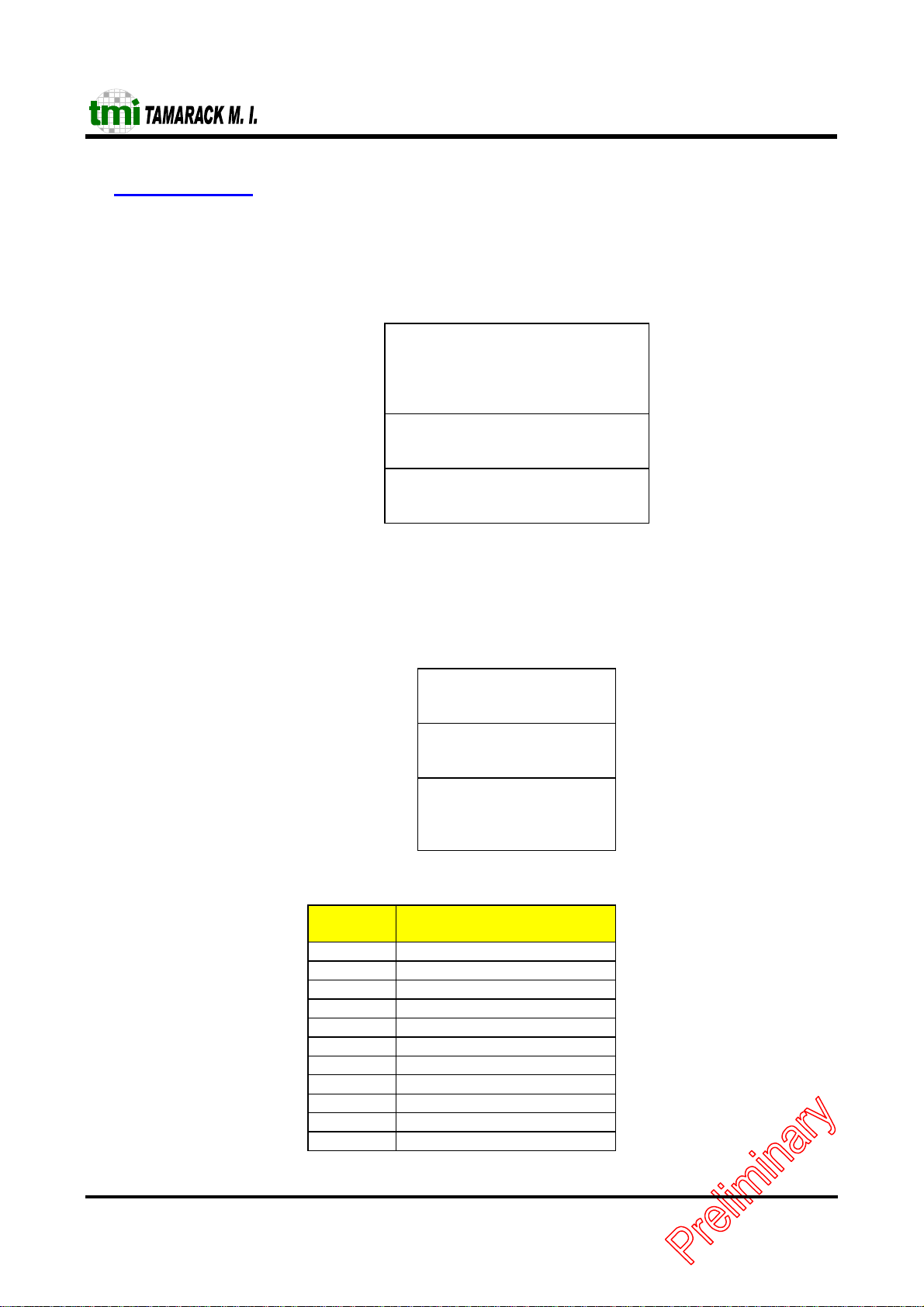
Figure 1 shows how the RESET circuitry operates.
VCC
RESET
TC5299J
Regload
EEload
The TC5299J Controller use a 93C56/66 EEPROM, The programmed contents of the EEPROM is shown as
following.
D15 D8 D7 D0
CIS byte n CIS byte n-1
13H ........ ........
12H ........ ........
11H CIS byte 3 CIS byte 2
10H CIS byte 1 CIS byte 0
0FH Not Used Config C
0EH Config. B Config. A
::::: Reserved Reserved
08H 42H 42H
07H 57H 57H
::::: Reserved Reserved
04H Reserved Reserved
03H Reserved bit [0]: 8-bit enable
bit [7:1]: Reserved
02H
01H
00H
Enet Address 5 Enet Address 4
Enet Address 3 Enet Address 2
Enet Address 1 Enet Address 0
EEPROM Programming Map
-8-
Ver. 0.1
07/04/01
Page 9

Storing and Loading Configuration from EEPROM:
During boot up the TC5299J Controller's configuration is read from the EEPROM, before the PROM data is read. The
configuration data is stored within the address 0EH, 0FH (as above table) of the EEPROM's address space.
Configuration Register A, B and C are located in the address 0EH.
To write this configuration into the EEPROM, the user can program register in TC5299J's address 02H of page 3. This
operation will work regardless of the level on EECONFIG.
TC5299J
-9-
Ver. 0.1
07/04/01
Page 10
TC5299J
4 I/O and Mapping
4.1 I/O Port Address M apping
This chip is register-liked with Novell's NE2000. The base I/O address of TC5299J Controller is configured by
Configuration Register (either upon po wer up or by software writing to this register). At that address the following
structure appears.
Base+00H
Base+0FH
Base+10H
Base+17H
Base+18H
Base+1FH
The registers within this area are 8 bits wide, but the data transfer port is 16 bits wide. By accessing the data transfer
port (using I/O instructions) the user can transfer data to or from the TC5299J 's internal memory.
4.2 EEPROM/SRAM Memory Mapping
The TC5299J Controller's internal memory map is as shown below.
D15 D7 D0
0000H
001FH
4000H
7FFFH
TC5299J Core Memory Map
PROM
Location
00h ETHERNET ADDRESS 0
01h ETHERNET ADDRESS 1
02h ETHERNET ADDRESS 2
03h ETHERNET ADDRESS 3
04h ETHERNET ADDRESS 4
05h ETHERNET ADDRESS 5
06-0Dh RESERVED
0E,0Fh 57h
10-15h ETHERNET ADDRESS 0-5
16-1Dh RESERVED
1E-1Fh 42h
Contents of PROM Map
Data Transfer Port
Location Contents
TC5299J
Core
Registers
Reset Port
PROM
Reserved
8K x 16
Buffer RAM
-10-
Ver. 0.1
07/04/01
Page 11

TC5299J Controller actually has 32k-address range but only does partial decoding on these devices. 0000H – 001FH is
PROM address and 4000H – 7FFFH is Buffer RAM address, otherwise is reserved. To access either the PROM or the
RAM buffer which user must initiate a Remote DMA transfer b etween the I/O port and memory.
Remote Read/Write Cache:
The TC5299J Controller includes 4 words cache internally. On a remote read the TC5299J Controller moves data from
memory buffer to the cache buffer; the TC5299J moves data continuously until the cache buffer is full. On a remote
write the system can writes data into the cache buffer until the 4 words cache buffer is full.
4.3 Attribute Memory Mapping
PCMCIA CIS Structures & Decode Function:
The TC5299J supports access to 1K of attribute Memory. Attribute memory is defined by the PCMCIA standard to be
comprised of the card information structure and four 8-bits Card Configuration Registers. These four registers are
contained in the TC5299J.
4.3.1 Attribute Memory Map
The attribute Memory map for a PCMCIA card is shown below.
Address Description
00H-3E0H Attribute Memory
3F0H (CCR4) I/O Event indication Register
3F2H (CCR5) Control Registe r
3F4H-3F6H Reserved
3F8H(CCR0) Configuration Option Register
3FAH(CCR1) Card Configuration and Status Register
3FCH(CCR2) Pin Replacement Register
3FEH(CCR3) Reserved
Card Option Registers 0 (R/W): 3F8H (CCR0)
D7 D6 D5 D4 D3 D2 D1 D0
SRESET XX PCMIOEN XX XX XX PJ1 PJ0
Name Description
PJ0-PJ1 If JMP1 pulled low during power on reset and FUNC=0, The two bits select one of
4 I/O base address. (shows as below)
PCMIOEN To set high make the card enter I/O mode. The function also can be set by JMP0
(MCS) when Power On Reset.
SRESET Setting this bit to high, place the card enter reset mode.
XX Reserved
JMP1 does not pull-low during power on reset.
TC5299J
-11-
Ver. 0.1
07/04/01
Page 12

Ethernet I/O address range
PJ1 PJ0 Address Range
0 0 300H-31FH
0 1 320H-33FH
1 0 340H-35FH
1 1 360H-37FH
Card Configuration and Status Registers (R/W): 3FAH (CCR1)
D7 D6 D5 D4 D3 D2 D1 D0
XX XX XX XX XX XX Ireq XX
Name Description
Ireq Interrupt. This bit describes the interrupt signal of LAN or MODEM
1: LAN interrupt
0: Modem interrupt
XX Reserved
TC5299J
-12-
Ver. 0.1
07/04/01
Page 13

5 Configuration Registers
5.1 Configuration Register A
To prevent any accidental writes of this register it is”hidden” behind a previous ly unused register. Re gister 0 AH
in the Controller's Page 0 of registers was previously reserved on a read. Now Configuration Register A can be
read at that address and can be written to by following a read to 0AH with a write to 0AH. If any other Contro ller
register accesses take place between the read and the write then the write to 0AH will access the Remote Byte
Count Register 0.
7 6 5 4 3 2 1 0
XX FREAD FDUPLEX LNK_CFG FULL_CFG IO16CON MIISEL1 MIISEL0
Name R/W Description
MIISEL[1:0] R/W 10: Default value to active t he MII bus.
Other: reserved.
IO16CON R/W When this bit is set high the Controller generates IO16 * after REG* active. If low this
output is generated only on address decode.
FULL_CFG R/W The bit is described EXLEDF what the polarity is.
0: Low active/ Hi inactive
1: Hi active/ Low inactive
LNK_CFG R/W The bit is described EXLEDL what the polarity is.
0: Low active/ Hi inactive
1: Hi active/ Low inactive
FDUPLEX R The Full-Duplex setting bit.
1: Full-duplex mode,
0: Half-duplex mode
PCMIOALL EL The bit is indicated the decode-number of SA[9:0].
0: Only decode 5 address-lines, SA[5:0].
1: Full decode 10 address-lines, SA[9:0].
FREAD R/W The TC5299J Controller supports 4 words Remote DMA read/write cache. When this
bit is set high, Remote DMA cache control will be enabled.
XX Reserved
TC5299J
PS. EL: The bit only set on EEPROM loading.
5.2 Configuration Register B
To prevent any accidental writes of his register it is ”hidden” behind a previously unused register. Register 0BH in
the Controller's Page 0 of registers was previously reserved on a read. Now Configuration Register B can be read
at that address and can be written to by following a read to 0BH with a write to 0BH. If any other Controller
register accesses take place between the read and the write then the write to 0BH will access the Remote Byte
Count Register 1.
7 6 5 4 3 2 1 0
XX LINT EXTRMII MIICINT MIICIM LINK LCINT LCIM
Name R/W Description
LCIM R/W The interrupt mask bit for link status changed. When set to “1”, the Interrupt will
generate on link status changed
.
-13-
Ver. 0.1
07/04/01
Page 14

LCINT R/W The Link-Changed interrupt report bit.
1: indicates the Link status changed.
LINK R When this bit is high, link test integrity checking is good. Otherwise, indicate link
signal lost.
MIICIM R/W This bit should be set to 0.
MIICINT R/W This bit should be set to 0.
EXTRMII R This bit should be set to 0.
LINT R/W LAN interrupt status indicator. To write a one to this bit can reset it.
XX X Reserved
5.3 Configuration Register C
This register just set in EEPROM and it can’t been read from user.
7 6 5 4 3 2 1 0
XX XX XX FE RBHI1 RBHI0 RBLO1 RBLO0
Name R/W Description
TC5299J
RBLO [1:0] X This is low value of receive buffer setting on full-duplex flow-control. It means that
are few data in Rx buffer.
00: Less than 1.5K data in Rx buffer.
01: Less than 3k data in Rx buffer.
10: Less than 4.5k data in Rx buffer.
11: Less than 6k data in Rx buffer.
RBHI [1:0] X That is high value of receive buffer setting on full-duplex flow-control. It means that is
few space in Rx buffer.
00: Less than 1.5K space in Rx buffer.
01: Less than 3k space in Rx buffer.
10: Less than 4.5k space in Rx buffer.
11: Less than 6k space in Rx buffer.
FE X Flow control enable bit in full-duplex mode.
0: Disable flow-control.
1: Enable flow-co n trol.
XX X Reserved
PS. X: Can’t read, just set these bit in the EEPROM.
5.4 Hardware Configuration
These functions are configured during a power on RESET.
Symbol I/O Description
JMP0 I/O Power on setting:
0: Enter I/O mode (Same as CCR0, bit 5)
JMP1 I/O Power on setting:
1: Full address decode(A9-A0)
0: Separate address decode(A5-A0)
-14-
Ver. 0.1
07/04/01
Page 15

Programming Register (R/W)
The Controller enable software (driver) pro gramming EEPR OM or testi ng in terrupt si gnal through thi s register d irectl y.
It is located at core register Page3 base+02H.
7 6 5 4 3 2 1 0
EESEL FIRQ XX READ CS SK DI DO(r) ATTRDIS
Name Description
TC5299J
EESEL,
CS,
SK,
DI,
DO
FIRQ This chip interrupt signal IRQ will be asserted when this bit is set high.
READ TC5299J can reload CFGA, CFGB and inter nal PROM, if this bit is set high. When reload
ATTRDIS Attribute and common memory access will be disable if it is programmed to high.
5.5 MII/PHY Control Register
The controller can access PHYTER register via software driver. It is located at core register Page3 base+03H.
Name R/W Description
MDC W MII Management Clock
The software can read or programming serial EEPROM directly through accesses these bits.
EESEL should be set high before starting the EEPROM read/write.
state is completed, READ will be cleared to low.
NOTE:
DO: read only
ATTRDIS: write only
7 6 5 4 3 2 1 0
XX FE XX XX MDI MDIR MDO MDC
MDO W MII Management Write Data.
MDIR W MII Management Operation Mode
Defines the operation of PHY.
When set, the PHY is in read operation mode.
When clear, the PHY is in write operation mode.
MDI R MII Management Data In.
FE R/W Flow control enable bit in full-duplex mode. The bit can be set when EEPROM
loading.
0: Disable flow-control.
1: Enable flow-co n trol.
XX X Reserved
5.6 TC5299J Core Registers Assignment
All registers are 8-bit wide and mapped into four pages, which are selected in the Command Register (PS0, PS1).
-15-
Ver. 0.1
07/04/01
Page 16

Pins A0-A3 are used to address registers within each page. Page 0 register are those registers which are commonly
accessed during TC5299J Controller operation while Page 1 registers are used primarily for initialization. The
registers are partitioned to avoid having to perform two read/write cycles to access commonly used registers.
Register Assignments:
Page 0 Address Assignments ( PS1=0,PS0=0)
A0-A3 RD WR
00H Command(CR) Command(CR)
01H Current Local DMA Address 0 (CLDA0) Page Start Register (PSTART)
02H Current Local DMA Address 1 (CLDA1) Page Stop Register (PSTOP)
03H Boundary Pointer (BNRY) Boundary Pointer (BNRY)
04H Transmit Status Register(TSR) Transmit Page Start Address (TPSR)
05H Number of Collisions Register(NCR) Transmit Byte Count Register 0 (TBCR0)
06H FIFO(FIFO) Transmit Byte Count Register 1 (TBCR1)
07H Interrupt Status Register(ISR) Interrupt Status Register(ISR)
08H Current Remote DMA Address 0(CRDA0) Remote Start Address Register 0(RSAR0)
09H Current Remote DMA Address 1(CRDA1) Remote Start Address Register 1(RSAR1)
0AH Config. Register A (CFGA) Remote Byte Count Register 0(RBCR0)
0BH Config. Register B (CFGB) Remote Byte Count Register 1(RBCR1)
0CH Receive Status Register(RSR) Receive Configuration Register(RCR)
0DH Tally Counter 0(Frame alignment Errors)
(CNTR0)
0EH Tally Counter 1 (CRC err ors) (CNTR1) Data Configuration Register(D CR)
0FH Tally Counter 2 (Missed Packet Errors)
(CNTR2)
Page 1 Address Assignments ( PS1=0,PS0=1)
A0-A3 RD WR
00H Command(CR) Command(CR)
01H Physical Address Register 0(PAR0) Physical Address Register 0(PAR0)
02H Physical Address Register 1(PAR1) Physical Address Register 1(PAR1)
03H Physical Address Register 2(PAR2) Physical Address Register 2(PAR2)
04H Physical Address Register 3(PAR3) Physical Address Register 3(PAR3)
05H Physical Address Register 4(PAR4) Physical Address Register 4(PAR4)
06H Physical Address Register 5(PAR5) Physical Address Register 5(PAR5)
07H Current Page Register(CURR) Current Page Register(CURR)
08H Multicast Address Register 0(MAR0) Multicast Address Register 0(MAR0)
09H Multicast Address Register 1(MAR1) Multicast Address Register 1(MAR1)
0AH Multicast Address Register 2(MAR2) Multicast Address Register 2(MAR2)
0BH Multicast Address Re gis ter 3(MAR3) Multicast Address Register 3(MAR3)
0CH Multicast Address Re gis ter 4(MAR4) Multicast Address Register 4(MAR4)
0DH Multicast Address Register 5(MAR5) Multicast Address Register 5(MAR5 )
Transmit Configuration Register(TCR)
Interrupt Mask Register(IMR)
TC5299J
-16-
Ver. 0.1
07/04/01
Page 17

Page 1 Address Assignments ( PS1=0,PS0=1)
A0-A3 RD WR
0EH Multica st Address Register 6(MAR6) Multicast Address Register 6(MAR6)
0FH Multicast Address Register 7(MAR7) Multicast Address Register 7(MAR7)
Page 2 Address Assignments ( PS1=1,PS0=0)
A0-A3 RD WR
00H Command(CR) Command(CR)
01H Page Start Register (PSTART) Current Local DMA Address 0(CLDA0)
02H Page Stop Register (PSTOP) Current Local DMA Address 1(CLDA1)
03H Remote Next Packet Pointer Remote Next Packet Pointer
04H Transmit Page Start Address(TPSR) Reserved
05H Local Next Packet Pointer Local Next Packet Pointer
06H Address Counter (Upper) Address Counter (Upper)
07H Address Counter (Lower) Address Counter (Lower)
08H Reserved Reserved
09H Reserved Reserved
0AH Reserved Reserved
0BH Reserved Reserved
0CH Receive Configuration Register(RCR) Reserved
0DH Transmit Configuration Register(TCR) Reserved
0EH Data Configuration Register(DCR) Reserved
0FH Interrupt mask Register(IMR) Reserved
Note: Page 2 registers should only be accessed for diagnostic purposes. They should not be modified during normal
operation. Page 3 Reserved should never be modified.
Page 3 Address Assignments (PS1=1,PS0=1)
A0-A3 RD WR
00H Command(CR) Command(CR)
01H Reserved Reserved
02H Progr ammi ng Re g. Programmi ng Reg.
03H MII Control Register MII Control Regi ster
04H Reserved Reserved
05H Reserved Reserved
06H Reserved Reserved
07H Reserved Reserved
08H Reserved Reserved
09H Reserved Reserved
0AH Reserved Reserved
0BH Reserved Reserved
TC5299J
-17-
Ver. 0.1
07/04/01
Page 18

Page 3 Address Assignments (PS1=1,PS0=1)
A0-A3 RD WR
0CH Reserved Reserved
0DH Reserved Reserved
0EH Reserved Reserved
0FH Reserved Reserved
5.7 Register Descriptions
5.7.1 Command Register (CR) 00H (Read/Write)
The Command Register is use d to initiate trans missions, enable or disable Remote DM A operations and
to select register pages. To issue a command the microprocessor sets the corresponding bit(s) (RD2,
RD1, RD0 and TXP). Further commands may be overlapped, but with the following rules: (1) if a
transmit command overlaps with a remote DMA operation, bits RD0, RD1, and RD2 must be maintained
for the remote DMA command when setting the TXP bit. Note, if a remote DM A command is re-issued
when giving the transmit command, the DMA will complete immediately if the remote byte count
register have not been reinitialized. (2 ) If a remote DMA operation overlap s a transmission, RD0, RD1 ,
and RD2 may be written with the desir ed values and a ”0”to this bit has no effect. (3) A remote write
DMA may not overlap remote read operation or visa versa. Either of these operations must either
complete or be aborted before the other operation may start. Bits PS1, PS0, RD2, and STP may be set
any time.
7 6 5 4 3 2 1 0
PS1 PS0 RD2 RD1 RD0 TXP STA STP
Bit Symbol Description
D0 STP Stop: Software reset command, take the controller offline, no packets will be
received or transmitted. Any reception of transmission in progress will continue to
completion before entering the reset state. T o exit this state, the STP bit must be
reset. The software reset has executed only when indicated by the RST bit in the
ISR being set to a 1. STP powers up high.
D1 STA Start: This bit is used to active the TC5299J core after either power up, or when the
TC5299J core has been placed in a reset mode by software command. STA power
up low.
D2 TXP T ransmit Packet: This bit must be set to initiate transmission of a packet. TXP is
internally reset either after the transmission is completed or aborted. This bit
should be set only after the Transmit Byte Count and Tr ansmit Page Start registers
have been programmed. TXP powers up low.
D3-D5 RD0-RD2 Remote DMA Command: These three encoded bits control operation of the
Remote DMA channel. RD2 can be set to about any Remote DMA command in
progress. The Remote Start Addresses are not restored to the starting address if the
Remote DMA is aborted. RD2 powers up high.
RD2 RD1 RD0
0 0 0 Not Allowed
0 0 1 Remote Read
0 1 0 Remote Write (Note)
0 1 1 Send Packet
1 X X Abort/Complete Remote DMA (Note)
D6,D7 PS0,PS1 Page Select: Three two encoded bits select which register page is to be accessed
with addresses A0-3.
PS1 PS0
0 0 Register Page 0
-18-
TC5299J
Ver. 0.1
07/04/01
Page 19

Bit Symbol Description
0 1 Register Page 1
1 0 Register Page 2
1 1 Register Page 3
5.7.2 Data Configure register (DCR) 0EH(Write)
This Register is used to program the TC5299J for 8 or 16-bit memory interface, select byte ordering in
16-bit applications and establish FIFO thresholds. The DCR must be initialized prior to loading the
Remote Byte count Registers.
7 6 5 4 3 2 1 0
- FT1 FT0 - LS - - WTS
Bit Symbol Description
D0 WTS Word Transfer Select
0: Selects byte-wide DMA transfers.
1: Selects word-wide DMA transfers
Note:
When word-wide mode is selected, up to 32k bytes are addressable; A0
remains low.
D1 - Reserved
D2 - Reserved
D3 LS Loopback Select
0: Loopback mode selected. Bits D1, D2 of the TCR must also be programmed for
Loopback mode selected.
1: Normal Operation.
D4 - Reserved
D5,D6 FT0,FT1 FIFO Threshold Select: Encoded: FIFO threshold. During reception, the FIFO
threshold indicates the number of bytes (or words) the FIFO has filled serially from
the network before the FIFO is emptied onto memory bus.
RECEIVE THRESHOLDS
FT1 FT0 Word Wide Byte Wide
0 0 2 Word 4 Bytes
0 1 4 Word 8 Bytes
1 0 8 Word 16 Bytes
1 1 12 Word 24 Bytes
During transmission, the FIFO threshold indicates the number of bytes (of words)
the FIFO has filled from the Local DMA before being transferred to the memory.
Thus, the transmission threshold is 16 bytes less the receive threshold.
5.7.3 Transmit configuration Register (TCR) 0DH(Write)
The transmit configuration establishes the actions of the transmitter section of the TC5299J during
transmission of a packet on the network, LB1 and LB0 power up as 0.
7 6 5 4 3 2 1 0
- - - OFST ATD LB1 LB0 CRC
Bit Symbol Description
D0 CRC Inhibit CRC
TC5299J
-19-
Ver. 0.1
07/04/01
Page 20

0: CRC appended by transmitter
1: CRC inhibited by transmitter
D1,D2 LB0,LB1 Encoded Loopback Control: These encoded configuration bits set the type of
loopback that is to be performed. Note that loopback in mode 2 sets the LPBK pin
high, this places the TC5299J in loopback mode and that D2 of the DCR must be
set to zero for loopback operation.
LB1 LB0
Mode0 0 0 Normal Operation (LPBK=0)
Mode1 0 1 Internal Loopback (LPBK=0)
Reserved 1 0
Reserved 1 1
D3 - Reserved
D4 OFST Collision Offset Enable: This bit modifies the back off algorithm to allow
prioritization of nodes.
0: Backoff Logic implements normal algorithm.
1: Forces Backoff algorithm modification to 0 to 2
mim(3+n,10)
slot times for first three
collisions, Then follows standard backoff. (For first three collisions station has
higher average backoff delay making a low priority mode.)
D5 - Reserved
D6 - Reserved
D7 - Reserved
5.7.4 Transmit Status Register (TSR) 04H(Read)
This register records events that occur on the media during transmission of a packet. It is cleared, when
the next transmission is initiat ed by the host. All bits remain lo w unless the event that cor responds to a
particular bit occurs during transmission. Each transmission should be followed by a read of this register.
The contents of this register are not specified until after the first transmission.
7 6 5 4 3 2 1 0
OWC FU CRS ABT COL - PTX
Bit Symbol Description
D0 PTX Packet Transmitted: Indicates transmission without error (No excessive collisions
or FIFO underrun) (ABT=”0”, FU=”0”).
D1 - Reserved
D2 CO L Transmit Collided: Indicates that the transmission collided at least once with
another station on the network. The number of collisions is recorded in the
Number of Collisions Registers. (NCR).
D3 ABT Transmit Aborted: Indicates the TC5299J aborted transmission because of
excessive collisions. (Total number of transmissions includin g or iginal
transmission attempt equals 16).
D4 CRS Carrier Sense Lost: This bit is set when carrier is lost during trans mis sion of the
packet. Carrier Sense is monitored from the end of Preamble/Synch until TXE is
dropped. Transmission is not aborted on loss of carrier.
D5 FU FIFO Underrun: If the TC5299J cannot gain access of the bus before the FIFO
empties, this bit is set. Transmission of the packet will be abo r ted.
D6 - Reserved
D7 OWC Out of Window Collision: Indicates that a collision occurred after a slot time.
Transmissions rescheduled as in normal collisions.
TC5299J
-20-
Ver. 0.1
07/04/01
Page 21

5.7.5 Receive Configuration Register (RCR) 0CH(Write)
This register determines operation of the TC5299J during reception of a packet and is used to program
what types of packets to accept.
7 6 5 4 3 2 1 0
- - MON PRO AM AB AR SEP
Bit Symbol Description
D0 SEP Save Errored Packets
0: Packets with receive errors are rejected.
1: Packets with receive errors are accepted. Receive errors are CRC and Frame
Alignment errors.
D1 AR Accept Runt Packets
0: Packets with fewer than 64 bytes rejected.
1: Packets with fewer than 64 bytes accepted.
D2 AB Accept Broadcast
0: Packets with all 1's broadcast destination address rejected.
1: Packets with all 1's broadcast destination address accepted.
D3 AM Accept Multicast
0: Packets with multicast destination address not checked.
1: Packets with multicast destination address c hecked.
D4 PRO Promiscuous Physical
0: Physical address of node must match the station address programmed in
PAR0-PAR5. (Physical address checked)
1: All packets with any physical address accepted. (physical address not
checked)
D5 MON Monitor Mode: Enables the receiver to check addresses and CRC on incoming
packets without buffering to memory. The missed packet Tally counter will be
incremented for each recognized packet.
0: Packets buffered to memory.
1: Packets checked for address match, good CRC and frame Alignment but not
buffered to memory.
D6 - Reserved
D7 - Reserved
Note:
D2 and D3 are ”OR'd” together, i. e., if D2 and D3 are set the TC5299J will accept broadcast and
multicast addresses as well as its o wn physical address. T o establish full pr omiscuous mode, b its D2, D3
and D4 should be set. In addition the multicast hashing array must be set to all 1's in order to accept all
multicast addresses.
5.7.6 Receive Status Register (RSR) 0CH(Read)
This register records status of the received packet, including information on errors and the type of
address match, either physical or multicast. The contents of this register are written to buffer memory by
the DMA after reception of a good packet. If packets with errors are to be saved the receive status is
written to memory at the head of the erroneous packet if an erroneous packet is received. If packets with
errors are to be rejected the RSR will not be written to memory. The contents will be cleared when the
next packet arrives. CRC errors, frame Alignment errors and missed packets are counted internally by
the TC5299J which relinquishes the Host from reading the RSR in real time to record errors for Network
Management functions. The contents of this register are not specified until after the first reception.
7 6 5 4 3 2 1 0
TC5299J
-21-
Ver. 0.1
07/04/01
Page 22

DFR DIS PHY MPA FO FAE CRC PRX
Bit Symbol Description
D0 PRX Packet Received Intact: Indicates packet received without error. (Bits CRC, FAE,
FO and MPA are zero for the received packet.)
D1 CRC CRC Error: Indicates packet received with CRC error. Increments Tally Counter
(CNTR1). This bit will also be set for Fra me Align ment errors.
D2 FAE Frame Alignment Error: Indicates that the incoming packet did not end on a byte
boundary and the CRC did not match at last byte boundary. Increments Tally
counter (CNTR0).
D3 FO FIFO Overrun: This bit is set when the FIFO is not serviced causing overflow
during reception. Reception of the packet will be aborted.
D4 MPA Missed Packet: Set when packet intended for node cannot be accepted by TC5299J
because of a lack of receive buffers of if the controller is in monitor mode and did
not buffer the packet to memory. Increments Tally Counter (CNTR2).
D5 PHY Physical/Multicast Address: Indicates whether received packet had a physical or
multicast address type
0: Physical Address Match
1: Multicast/Broadcast Address Match
D6 DIS Receiver Disabled: Set when receiver disabled by entering Monitor mode. Reset
when receiver is re-enabled when exiting Monitor mode.
D7 DFR Deferring: Set when CRS or COL inputs are active. If the transceiver has asserted
the CD line as a result of the jabber, this bit will stay set indicatin g the jabber
condition.
Note: Following coding applies to CRC and FAE bits
FAE CRC Type of Error
0 0 No error (Good CRC and <6 Dribble Bits)
0 1 CRC ERROR
1 0 Legal, will not occur
1 1 Frame Alignment Error and CRC Error
5.7.7 Interrupt Mask Register (IMR) 0FH(Write)
The interrupt Mask Register is used to mask interrupts. Each interr upt mask bit corresponds to a bit in
the Interrupt Status Register (ISR). If an interrupt mask bit is set, an interrupt will be issued whenever
the corresponding bit in the I SR is set. If any bit in the IMR is set low, a n interrupt will not o ccur when
the bit in the ISR is set. The IMR powers up all zeroes.
7 6 5 4 3 2 1 0
- RDCE CNTE OVWE TXEE RXEE PTXE PRXE
Bit Symbol Description
D0 PRXE Packet Received Interrupt Enable: Enables Interrupt when packet received.
D1 PTXE Packet Transmitted Interrupt Enable: Enables Interrupt when packet is tra nsmit ted.
D2 RXEE Receive Error Interrupt Enable: Enables Interrupt when packet received with error.
D3 T X EE Transmit Error Interrupt Enable: Enables Interrupt when packet transmissio n
results in error.
D4 OVWE Over Write Warning Interrupt Enable: Enables Interrupt when Buffer management
Logic lacks sufficient buffers to store incoming packet.
D5 CNTE Counter Overflow Interrupt Enable: Enables Interrupt when MSB of one or more
TC5299J
-22-
Ver. 0.1
07/04/01
Page 23

Bit Symbol Description
of the Network Tally counters has been set.
D6 RDCE DMA Complete Interrupt Enable: Enables Interrupt when Remote DMA transfer
has been completed.
D7 - Reserved
5.7.8 Interrupt Status Register (ISR) 07H(Read/Write)
This register is accessed to determine the cause of an interrupt. Any interrupt can be masked in the
interrupt Mask Register (IMR). Individual interrupt bits are cleared by writing a ”1” into the
corresponding bit of the ISR.
The IRQ signal is active as long as any unmasked signal is set, and will not go lo w until all unmarked
bits in this register have been cleared. The ISR must be cleared after power up by writing it with all 1's.
7 6 5 4 3 2 1 0
RST RDC CNT OVW TXE RXE PTX PRX
Bit Symbol Description
D0 PRX Packet Received: Indicates packet received with no errors.
D1 PT X Packet Transmitted: Indicates packet transmitted with no erro r s.
D2 RXE Receive Error: Indicates that a packet was received with one or more of the
following errors:
- CRC Error
- Frame Alignment Error
- FIFO Overrun
- Missed Packet
D3 T XE Transmit Error: Set when packet transmitted with one or more of the following
errors:
- Excessive Collisions
- FIFO Underrun
D4 OVW Over Write Warning: Set when receive buffer ring storage resources have been
exhausted. (Local DMA has reached Boundary Pointer).
D5 CNT Counter Over flow: Set when MSB of one or more of the Network Tally Counters
has been set.
D6 RDC Remote DMA Complete: Set when Remote DMA oper ation has been completed.
D7 RST Reset Status: A status indicator with no interrupt generated
- Set when TC5299J enters reset state and is cleared when a start command is
issued
- Set when a Receive Buffer Ring overflows and is cleared when leaves
overflow status. Writing to this bit has no effe ct and powers up high.
5.8 Network Tally Counter Registers (CNTR)
Three 8-bit counters are provided for monitoring the number of CRC errors, Frame Alignment Errors and missed
packets, The maximum count reached by any counter is 192 (C0H). These registers will be cleared when read by
the CPU. The count is recorded in binary in CT0-CT7 of each Tally Register.
CNTR0: Monitor the number of Frame Alignment error
7 6 5 4 3 2 1 0
CT7 CT6 CT5 CT4 CT3 CT2 CT1 CT0
CNTR1: Monitor the number of CRC error
-23-
Ver. 0.1
07/04/01
TC5299J
Page 24

7 6 5 4 3 2 1 0
CT7 CT6 CT5 CT4 CT3 CT2 CT1 CT0
CNTR2: Monitor the number of Missed Packets
7 6 5 4 3 2 1 0
CT7 CT6 CT5 CT4 CT3 CT2 CT1 CT0
5.9 Number of Collisions Register (NCR)
This register contains the number of collisions a node experiences when attempting to transmit a packet. If no
collisions are experienced during a transmission attempt, the COL bit of the TSR will not be set and the contents of
NCR will be zero. If there are excessive collisions, the ABT bit in the TSR will be set and the contents of NCR
will be zero. The NCR is cleared after the TXP bit in the CR is set.
7 6 5 4 3 2 1 0
- - - - NC3 NC2 NC1 NC0
5.10 Physical Address Register (PAR0-PAR5)
The physical address registers are used to compare the destination address of incoming packets for rejecting or
accepting packets. Comparisons are performed on a byte-wide basis. The bit assignment shown below relates the
sequence in PAR0-PAR5 to the bit sequence of the received packet.
.. Syn Syn DA0 DA1 DA2 DA3 DA4 DA5 DA6 DA7 ..
|------- Destination Address --------|--- Source
D7 D6 D5 D4 D3 D2 D1 D0
PAR0 DA7 DA6 DA5 DA4 DA3 DA2 DA1 DA0
PAR1 DA15 DA14 DA13 DA12 DA11 DA10 DA9 DA8
PAR2 DA23 DA22 DA21 DA20 DA19 DA18 DA17 DA16
PAR3 DA31 DA30 DA29 DA28 DA27 DA26 DA25 DA24
PAR4 DA39 DA38 DA37 DA36 DA35 DA34 DA33 DA32
PAR5 DA47 DA46 DA45 DA44 DA43 DA42 DA41 DA40
5.11 Multicast Address Registers (MAR0-MAR7)
The Multicast address registers provide filtering of multica st addresses hashed by the CRC logic. All destination
addresses are fed through the CRC logic and as the last bit of the destination address enters the CRC, the 6 most
significant bits of the CRC generator are latched. These 6 bits are then decoded by a 1 of 64 decode to index a
unique filter bit (FB0-63) in the multicast address register. I f the filter bit selected is set, the multicast packet is
accepted. The system designer would use a program to determine which filter bits to set in the multicast registers.
For some address found to hash to the value 50 (32H), then FB50 in MAR6 should be initialized to ”1” All
multicast filter bits that correspond to multicast address ac cepted by the node are then set to one. To accept all
multicast packets all of the registers are set to all ones.
D7 D6 D5 D4 D3 D2 D1 D0
MAR0 FB7 FB6 FB5 FB4 FB3 FB2 FB1 FB0
MAR1 FB15 FB14 FB13 FB12 FB11 FB10 FB9 FB8
MAR2 FB23 FB22 FB21 FB20 FB19 FB18 FB17 FB16
MAR3 FB31 FB30 FB29 FB28 FB27 FB26 FB25 FB24
TC5299J
-24-
Ver. 0.1
07/04/01
Page 25

MAR4 FB39 FB38 FB37 FB36 FB35 FB34 FB33 FB32
MAR5 FB47 FB46 FB45 FB44 FB43 FB42 FB41 FB40
MAR6 FB55 FB54 FB53 FB52 FB51 FB50 FB49 FB48
MAR7 FB63 FB62 FB61 FB60 FB59 FB58 FB57 FB56
5.12 DMA Registers
LOCAL DMA TRANSMIT REGISTERS
15 8| 7 0
(TPSR) TRANSMIT
PAGE
START
(TBCR0,1) TRANSMIT BYTE COUNT
5.13 LOCAL DMA RECEIVE REGISTERS
15 8| 7 0
(PSTART) PAGE START
(PSTOP) PAGE STOP
(CURR) CURRENT
(BRNY) BOUNDARY
15 8| 7 0
(CLDA0,1) CURRENT LOCAL DMA
ADDRESS
5.14 REMOTE DMA REGISTERS
15 8| 7 0
(RSAR0,1) START ADDRESS
(RBCR0,1) BYTE COUNT
(CRDA0,1) CURRENT REMOTE DMA
ADDRESS
5.15 (i) Local DMA Transmit Registers
Transmit page start register (TPSR):
This register points to the assembled packet to be transmitted. Only the eight higher order addresses be specified since
all transmit packets are assembled on 256-byte page boundaries.
7 6 5 4 3 2 1 0
A15 A14 A13 A12 A11 A10 A9 A8
Transmit byte count register0, 1 (TBCR0, TBCR1):
These two registers indicate the length of the packet to be transmitted in bytes. The maximum number of transmit bytes
allowed is 32k bytes. (4000H – 7FFFH) The TC5299J will not truncate transmissions longer than 1500 bytes.
7 6 5 4 3 2 1 0
TBCR1 L15 L14 L13 L12 L11 L10 L9 L8
TC5299J
-25-
Ver. 0.1
07/04/01
Page 26

7 6 5 4 3 2 1 0
TBCR0 L7 L6 L5 L4 L3 L2 L1 L0
5.16 (ii) Local DMA Receive Registers
Page start, stop registers (PSTART, STOP):
The Page Start and Page stop Registers program the starting and stopping page of the Receive Buffer Ring. Since the
TC5299J uses fixed 256-byte buffers aligned on page boundaries only the upper eight bits of the start and stop address
are specified.
7 6 5 4 3 2 1 0
PSTART PSTOP A15 A14 A13 A12 A11 A10 A9 A8
Boundary register (BNRY):
This register is used to prevent overflow of the Receive Buffer Ring. Buffer management compares the contents of this
register to the next buffer address when linking buffers tog ether. If the contents of this register match the next buffer
address the local DMA operation is aborted.
7 6 5 4 3 2 1 0
BNRY A15 A14 A13 A12 A11 A10 A9 A8
5.17 (iii) Remote DMA registers
Remote Start Address Registers (RSAR0, 1):
Remote Byte Count Registers (RBCR0, 1):
Remote DMA operations are programmed via the Remote Start Address (RSAR0, 1) and Remote Byte Count (RBCR0,
1) registers. The Remote Start Address is used to point to the start of the block of data to be transferred and the Remote
Byte Count is used to indicate the length of the block (in bytes).
7 6 5 4 3 2 1 0
RSAR1 A15 A14 A13 A12 A11 A10 A9 A8
7 6 5 4 3 2 1 0
RSAR0 A7 A6 A5 A4 A3 A2 A1 A0
7 6 5 4 3 2 1 0
RBCR1 BC15 BC14 BC13 BC12 BC11 BC10 BC9 BC8
7 6 5 4 3 2 1 0
RBCR0 BC7 BC6 BC5 BC4 BC3 BC2 BC1 BC0
Current Page Register:
This register is used internally by the Buffer Management Logic as a backup register for reception. CURR contains the
address of the first buffer to be used for a packet reception and is used to restore DMA pointers in the event of receive
errors. This register is initialized to the same value as PST ART and should not be written to again unless the controller
is reset.
7 6 5 4 3 2 1 0
CURR A15 A14 A13 A12 A11 A10 A9 A8
TC5299J
-26-
Ver. 0.1
07/04/01
Page 27

Current local DMA register 0,1 (CLDA0, 1):
These two registers can be accessed to determine the current Local DMA Address.
7 6 5 4 3 2 1 0
CLDA1 A15 A14 A13 A12 A11 A10 A9 A8
7 6 5 4 3 2 1 0
CLDA0 A7 A6 A5 A4 A3 A2 A1 A0
Current Remote DMA Address Registers:
The Current Remote DMA Registers contain the current address of the Remote DMA. The bit assignment is shown as
below:
7 6 5 4 3 2 1 0
CRDA1 A15 A14 A13 A12 A11 A10 A9 A8
7 6 5 4 3 2 1 0
CRDA0 A7 A6 A5 A4 A3 A2 A1 A0
TC5299J
-27-
Ver. 0.1
07/04/01
Page 28

a
6 Electrical Specification and Timing
MII :
RECEIVE TIMING
An example transfer a packet from PHY to MAC
RXC
RXDV
TC5299J
RXD[3:0]
RXER
TRANSMIT TIMINGS
An example transfer a packet from MAC to PHY
TXC
TXEN
TXD[3:0]
CRS
COL
Receive Dat a
Transmit Dat
-28-
Ver. 0.1
07/04/01
Page 29

ISA Slave Accesses
TC5299J
ISA Slave Accesses
ALE
AEN
SA0-9
IOR*,IOW*
IO16*
IORDY
SD0-15
(Read)
T1
T19
T15
T2
T6c
T6a
T5a
T3 T4
T5c
T13
T17
T16
T18
T7
T14
T10
T9
T12
SD0-15
(Write)
T20
T11
Data Valid
MR*
T21
MW
*
T22
-29-
Ver. 0.1
07/04/01
Page 30

Symbol Description
T1 ALE Width (ISA Interface) 20 20 ns
T2 AEN valid before Command Strobe Active 60 60 ns
T3 SA0-9 Valid before IOR* , IOW* Asserted 40 20 ns
T4 IOR*, Asserted to SD0-15 Driven 0 0 ns
T5a SA0-9 Valid before IO16* Valid 60 ns
T5c SA0-9 Valid and IOR* or IOW* Active before IO16*
Valid
T6a IOR*, IOW* Asserted to IORDY Deasserted 100 50 ns
T6c ALE Asserted and SA0-9 Valid to IORDY Deasserted 60 60 ns
T7 IOR*, IOW* Deasserted before SA0-9 Invalid 15 15 ns
T9 IOR*, Deasserted to SD0-15 Read Data Invalid 0 0 ns
T10 IOR*, Deasserted to SD0-15 Floating 45 45 ns
T11 SD0-15 Write Data Valid to IOW* Deasserted 60 20 ns
T12 IOW*, Deasserted to SD0-15 Write Data Invalid 20 20 ns
T13 IOR*, IOW* Active Width 300 140 ns
T14 IOR*, IOW* Inactive Width 85 85 ns
T15 ALE Asserted before IOR*, IOW* Asserted 25 ns
T16 IOR*, IOW* Negated before Next ALE Asserted 20 ns
T17 IORDY Asserted to SD0-15 I/O Read Data Valid 60 60 ns
T18 IOR*, IOW* Deasserted before AEN Invalid 25 25 ns
T19 AEN Valid before ALE Deasserted 50 50 ns
T20 IOR* Asserted to SD0-15 Read Data Valid 150 90 ns
T21 IORDY Invalid after MR* Deasserted 30 ns
T22 IORDY Invalid after MW* Deasserted 20 ns
8-Bit Transfers 16-Bit Transfers
Min Max Min Max
50 ns
TC5299J
Units
-30-
Ver. 0.1
07/04/01
Page 31

7 Physical Dimension
TC5299J
D
1
D1
2
4
2
θ
1
θ
96
97
65
64
R1
B
R2
AA2
6
128
PIN 1
IDENTIFIER
A1
E1
2E1
B
S
3
33
θ
L
L1
DETAIL "A"
1
e
32
b
"A"
-C-
0.08
C
WITH PLATING
b
GAGE PLANE
.25
θ
35
PACKAGE LQFP 128
c
5
BASE
METAL
b1
SECTION B-B
Symbol
A
A1
A2
b 0.009
b1
c
c1
D 0.636
D1
E
E1 0.555
e
L
L1
R1
R2 0.008
S
θ
1
θ
2
θ
3
θ
Dimension in mm
Min
------
0.05
1.35
0.13
0.13 0.16
0.09
0.09
15.85
13.90 14.00
15.85
13.90
0.45 0.60
0.08
0.08
0.20 ------
0
0
°
°
12
12
Nom
------
------
1.40
0.18 0.23
------
------
16.00 16.15
16.00
14.00 14.10
0.40 BSC
1.00 REF
------
------ 0.20
------ -----TYP
°
°
Max
1.60
------
1.45
0.19
0.20
0.16
14.10
16.15
0.75
------
------
53 .
°
7
°
Dimension in inch
Nom
Min
0
°
°
------
------
0.055
0.007
0.006
------
------
0.630
0.551
0.630
0.551
0.016 BSC
0.024
0.039 REF
------
------
------
-----TYP
12
°
12
°
TYPTYP
------
0.002
0.053
0.005
0.005
0.004
0.004
0.624
0.547
0.624
0.547
0.018
0.003
0.003
0.008
0
Max
0.063
------
0.057
0.007
0.008
0.006
0.555
0.636
0.030
------
-----
53 .
°
7
°
------
c1
5
5
-31-
Ver. 0.1
07/04/01
Page 32

TC5299J
Notice
This document contains information on pr oduct, which is in the develop ment phase. TMI reserves the rights to change
specifications, features, functions and availability of the prod uct without notice.
TMI devices are NOT designed, intended, authorized, or warranted to be suitable for use in Life-Supporting
applications.
-32-
Ver. 0.1
07/04/01
 Loading...