

Page 1

TC520A
Serial Interface Adapter for TC500 A/D Converter Family
Features
• ConvertsTC500/TC500A/TC510/TC514 to Serial
Operation
• Programmable Conversion Rate and Resolution for
Maximum Flexibility
• Supports up to 17-Bits of Accuracy Plus Polarity Bit
• Low Power Operation: Typically 7.5mΩ
• 14-Pin PDIP or 16-Pin SOIC Packages
• Polled or Interrupt Mode Operation
Applications
• Computer Peripheral Interface
• PortableInstruments
• Data Acquisition System Interface
Device Selection Table
Part Number Package Temperature Range
TC520ACOE 16-Pin SOIC (Wide) 0°Cto+70°C
TC520ACPD 14-Pin PDIP 0°Cto+70°C
Package Type
14-Pin PDIP
V
114
DGND
CMPTR
OSC
OSC
DD
213
312
411
B
A
OUT
IN
TC520A
510
69
78
CE
DV
LOAD
D
IN
DCLK
D
OUT
READ
General Description
The TC520A serial interface adapter provides logic
control for Microchip's TC500/TC500A/TC510/TC514
family of dual slope, integrating A/D converters. It
directly manages TC500 converter phase control signals A, B and CMPTR, thereby reducing host
processor task loading and software complexity. Communication with the TC520A is accomplished over a 3
wire serial port. Key converter operating parameters
are programmable for complete user flexibility. Data
conversion is initiated when the CE
low. The converted data (plus overrange and polarity
bits) are held in an 18-bit shift register until r ead by the
processor or until the next conversion is completed.
Data may be clocked out of the TC520A at any time,
and at any rate, the userprefers.ADataValid (DV
put is driven active at the start of each conversion
cycle,indicatingthe 18-bit shift register update has just
been completed. This signal may be polled by the processor or can be used as data ready interrupt. The
TC520A timebase can be derived from an external frequency source of up to 6MHz or can operate from its
own externalcrystal.It requiresasingle5Vlogicsupply
and dissipates less than 7.5mΩ.
input is brought
)out-
16-Pin SOIC
V
DGND
CMPTR
OSC
OUT
OSC
N/C
2002 Microchip TechnologyInc. DS21431B-page 1
DD
1
2
3
4
B
TC520A
5
6
7
IN
8
16
15
14
13
12
11
10
9
CE
DV
LOAD
D
IN
DCLKA
D
OUT
READ
N/C
Page 2
TC520A
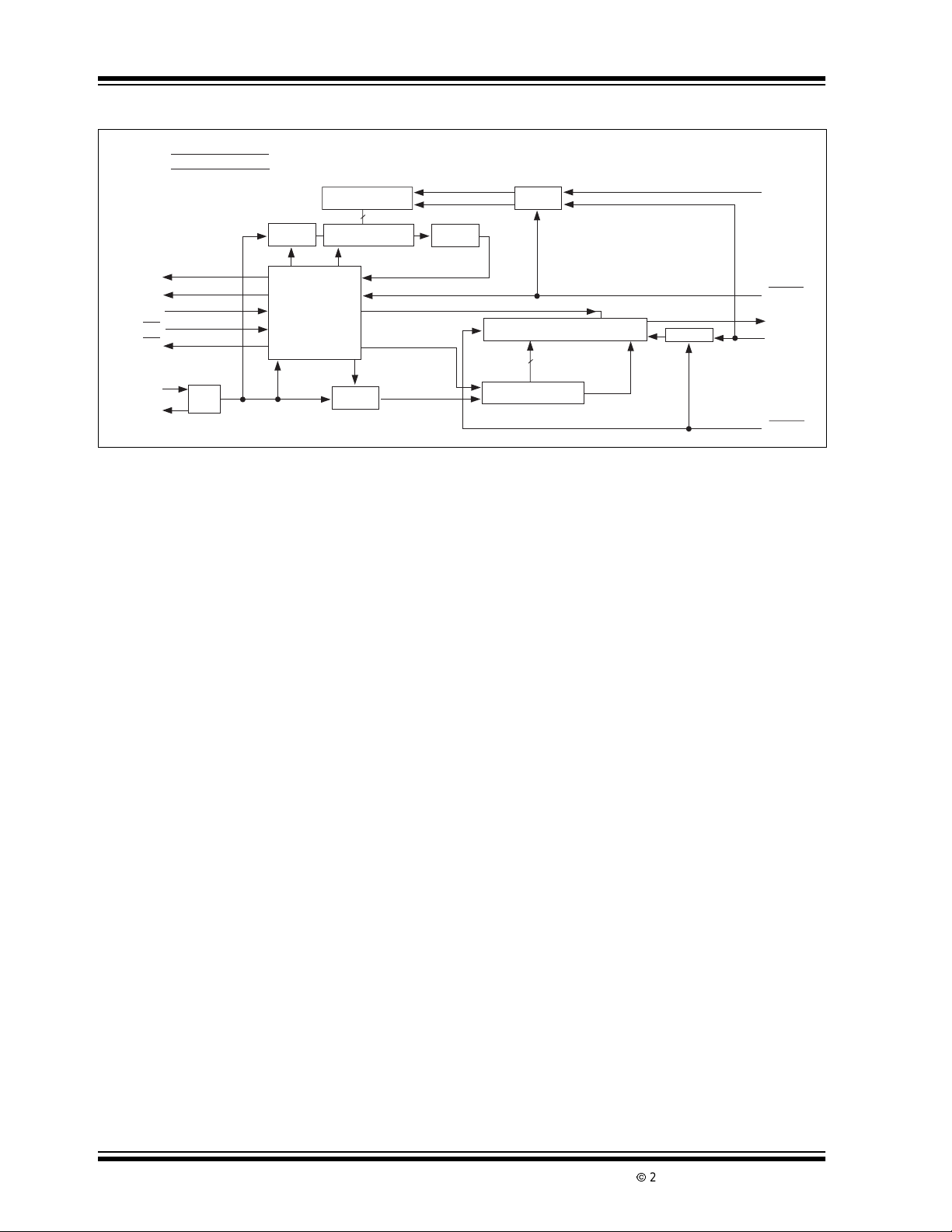
Functional Block Diagram
1
V
DD
2
GND
Gate
8-Bit Shift Reg.
8
8-Bit Counter
÷ 256
Gate
Pinout of 14-Pin
Package
11
D
IN
CMPTR
OSC
OSC
CE
DV
IN
OUT
Clear Count
Gate
Timeout
Force Auto Zero
Polarity Bit
18-Bit Shift Register
16
16-Bit Counter
Overrange
Bit
Gate
12
10
LOAD
9
D
OUT
D
CLK
8
READ
5
A
4
B
14
13
3
7
÷4
6
Logic Control
SYSCLK
DS21431B-page 2
2002 Microchip TechnologyInc.
Page 3
TC520A
1.0 ELECTRICAL
CHARACTERISTICS
*Stresses above those listed under "Absolute Maximum Ratings"maycause permanentdamage to thedevice.These are
stress ratings only and functional operation of the device at
these or any other conditions above those indicated in the
Absolute Maximum Ratings*
DC Supply Voltage (VDD)....................................+6.0V
Input Voltage (All Inputs V
Operating Temperature Range (T
):.... - 0.3V to (VDD+0.3V)
IN
) .......... 0°C to 70°C
A
operation sections of the specifications is not implied. Exposure to Absolute Maximum R ating conditions for extended
periodsmay affectdevice reliability.
StorageTemperature Range..............-65°Cto +150°C
TC520A E LECTRI CAL SPECIFICATIONS
Electrical Characteristics: VDD=5V,F
Symbol Parameters Min Typ Max Unit Test Conditions
Supply
V
DD
I
DD
Operating Voltage Range 4.5 5 5.5 V
SupplyCurrent — 0.8 1.5 mA
Input Characteristics
V
V
I
IL
I
PD
I
PU
Output Characteristics (I
V
OL
V
OH
T
R,TF
Oscillator (OSC
F
XTL
F
OSC
Low InputVoltage — — 0.8 V
IL
HighInputVoltage 2.0 — — V
IH
InputLeakage Current — — 10 µA
Pull-down Current (CE)—5—µA
Pull-up Current (READ,LOAD)—5—µA
=250µA, VDD=5V)
OUT
Low Output Voltage — 0.2 0.3 V
High Output Voltage 3.5 4.3 — V
CL= 10pF, Rise/Fall Times — — 250 nsec
,OSC
IN
OUT
)
Crystal Frequency — 1.0 4.0 MHz
External Frequency(OSCIN)——6.0MHz
Timing Characteristics
READ Delay Time 250 — — nsec
Data Read Setup Time 1 — — µsec
D
CLK
to D
Delay 450 — — nsec
OUT
LOAD Setup Time 1 — — µsec
Data Load Setup Time 50 — — nsec
D
Pulse Width Low Time 150 — — nsec
CLK
D
Pulse Width High Time 150 — — nsec
CLK
Load Default Low Time 250 — — nsec
Load Default Setup Time 250 — — nsec
T
T
T
T
T
T
T
T
DRS
T
DLS
PWL
PWH
LDL
LDS
RD
RS
LS
Parameter
T
T
AZI
IntegratorZERO Time — 0.5 — msec
IZ
Auto zero (RESET) Time at Power-Up — 100 — msec
=1MHz,TA= +25°C, unless otherwise specified.
OSC
2002 Microchip TechnologyInc. DS21431B-page 3
Page 4
TC520A
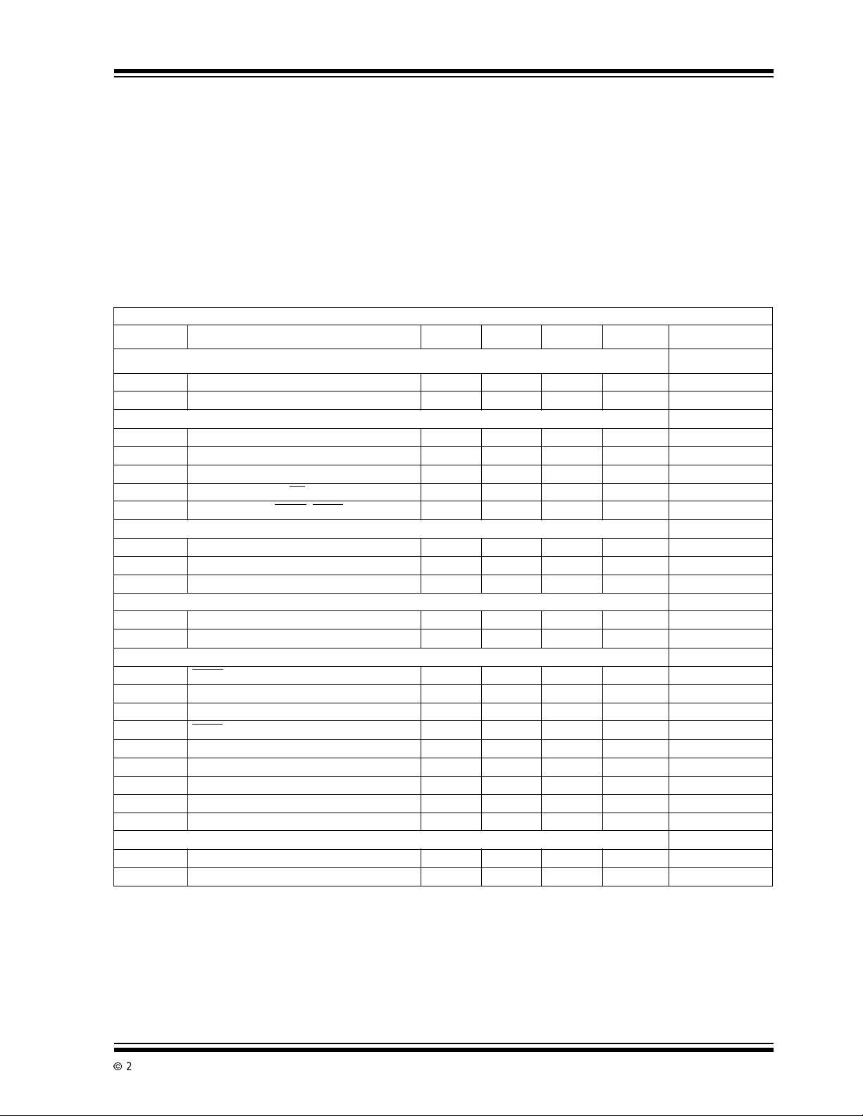
2.0 PIN DESCRIPTIONS
ThedescriptionsofthepinsarelistedinTable2-1
TABLE 2-1: PIN FUNCTION TABLE
Pin Number
14-Pin PDIP
11V
Pin Number
16-Pin SOIC
Symbol Description
Input. +5V ±10% power supply input with respect to DGND.
DD
2 2 DGND Input. Digital Ground.
3 3 CMPTR Input,active high or low (depending on polarity of the voltageinputtoA/D converter).
This pin connects directly to the zero crossing comparator output(CMPTR) of the
TC5XX A/D converter. A high-to-low state change on this pin causes the TC520A to
terminate the de-integrate phase of conversion.
4 4 B Output, active high. The A and B outputs of the TC520A connect directly to the A and B
inputs of the TC5XX A/D converter connected to the TC520A. The binary code on A, B
determines the conversion phase of the TC5XX A/D converter: (A, B) = 01 places the
TC5XX A/D converter into the Auto Zero phase; (A, B) =10 for Integrate phase (INT);
(A, B) =11 for De-integrate phase (DINI) and (A, B) = 00 for Integrator Zero phase (IZ).
Pleasesee the TC500/TC500A/TC510/TC514 family data sheetsfora complete
description of these phases of operation.
5 5 A Output, active high. See pin 4 description above.
66OSC
Input.Thispinconnects to one side of an AT-cut crystalhaving a effective series resis-
OUT
tance of 100Ω (typ.) and a parallel capacitance of 20pF (typ.). If an external frequency
sourceisused to clock the TC520A, this pin must be left floating.
77OSC
Input.Thispinconnects to the other side of the crystaldescribed in pin 6 above. The
IN
TC520Amayalsobe clocked from an external frequencysource connectedto thispin.
The externalfrequency source must be a pulse trainhaving a duty cycle of 30% (mini-
mum); rise and fall times of 15nsec and a min/max amplitude of 0 to V
frequency source is used, pin 6 must be left floating. A maximum operating frequency
.Ifanexternal
IH
of 4MHz (crystal) or 6MHz (external clock source) is permitted.
8 N/C No connection on 16 pin package version.
9 N/C No connection on 16 pin package version.
8 10 READ
Input, active low, level and negative edge triggered. A high-to-low transition on READ
loadsserial port output shiftregister with the most recent converted data.Datais
loaded such that the first bit transmitted from the TC520A to the processor is the
OVERRANGE bit (OVR), followed by the POLARITY bit (POL) (high = input positive;
low = input negative). This is followed by a 16-bit data word (MSB first). OVR is avail-
able at the D
data bit, if so desired. The D
held low. Otherwise, D
cycle is terminated at any time by bringing READ
911D
10 12 D
Output, logic level. Serialportoutput pin. This pin is enabled only when READ is low
OUT
(see READ
Input, positive and negative edge triggered. Serial port clock. With READ low, serial
CLK
dataisclocked into the TC520Aateachlow-to-high transitionof D
of the TC520A on each high-to-lowtransitionof D
as soon as READ is broughtlow. This bit may be used as the 17th
OUT
OUT
pin of the serial port is enabled only when READ is
OUT
remains in a high impedance state. A serial port read access
high.
pin description).
, and clockedout
.AmaximumserialportD
CLK
CLK
frequency of 3MHz is permitted.
11 13 D
Input, logic level. Serial port input pin. The TC5XX A/D converter integration time (T
IN
andAutoZero time (TAZ) values are determined by theLOADVALUEbyte clockedinto
this pin. This initialization must take place at power up and can be rewritten (or modified
and rewritten) at any time. The LOAD VALUE is clocked into D
MSB first.
IN
CLK
INT
)
DS21431B-page 4
2002 Microchip TechnologyInc.
Page 5

TABLE 2-1: PIN FUNCTION TABLE (CONTINUED)
TC520A
Pin Number
14-Pin PDIP
12 14 LOAD Input, active low; level and edge triggered. The LOAD VALUE is clocked into the 8-bit
13 15 DV
14 16 CE
Pin Number
16-Pin SOIC
Symbol Description
shiftregister on board the TC520A while LOAD
transferred into the TC520A internal timebase counter (and becomes effective) when
LOAD
is returned high. If so desired, LOAD can be momentarily pulsedlow,eliminating
theneedtoclockaLOADVALUEintoD
clocked into the TC520A timebase counter selecting either a count of 65536
(D
= High), or count of 32768, (DIN=Low).
IN
Output,active low. DV is brought low any time the TC520A is in the AZ phase of conversion. This occurs when, either the TC520A initiates a normal AZ phase by setting A,
B, equal to 01, or when CE
andforcesanAZstate.DV
Input,active low,leveltriggered.Conversion willbe continuously performed as long as
CE
remains low. Pulling CE high causes the conversion process to be halted and
forcestheTC520A into the AZ mode for as long as CE
takenhighwhenever it is necessary to momentarilysuspend conversion (for example:
to change the address lines of an input multiplexer). CE
whentheTC520A entersanAZphase(i.e. when DV
excessively long integrator discharge times, which could result in erroneous conversion. This pin should be grounded if unused. It should be left floating if a 0.01µF
RESETcapacitor is connected to it (see Section 4.0, Typical Applications).
is pulled high, which overrides the normal A, B sequencing
is returnedhighwhentheTC520A exits AZ.
. In this case, the current stateof DINis
IN
is held low. The LOAD VALUE is then
remains high. CE should be
should be pulled high only
is low). This is necessary to avoid
2002 Microchip TechnologyInc. DS21431B-page 5
Page 6

TC520A
3.0 DETAILED DESCRIPTION
3.1 TC520A Timing
The TC520A consists of a serial port and state
machine. The state machine provides control timing to
the TC5xx A/D converter connected to the TC520A as
well as providing sequential timing for TC520A internal
operation. All timing is derived from t he frequency
source at OSC
can be either an externally provided clock signal or
external crystal. If an external clock is used, it must be
connected to the OSC
floating. If a crystal is used, it must be connected
between t he OSC
located as close to the OSC
possible. The incoming frequency is internally divided
by 4 and the resulting clock (SYSCLK) controls all
timing functions.
3.2 TC5XX A/D Converter Control
Signals
The TC520A control outputs (A, B) and control input
(CMPTR) connect directly to the corresponding pins of
the TC5XX A/D converter. A conversion is consummated when A, B have been sequenced through t he
required 4 phases of conversion: Auto Zero (AZ), Integrate(INT),De-integrate(D
(see Figure 4-1). The Auto Zero phase compensates
for offset errors in the TC5XX A/D converter. The
Integrate phase connects the voltage to be converted
to the TC5XX A/D converter input, resulting in an integrator output dv/dt directly proportional to the magnitudeoftheappliedinputvoltage. ActualA/Dconversion
(counting)isinitiatedat the startof the DI NT phase and
terminates when the integrator output crosses 0V. The
integrator output is then forced to 0V during the IZ
phase and the c onverter is ready for another cycle.
Please see the TC500/TC500A/TC510/TC514 data
sheet for a complete description of these phases.
The number of SYSCLK periods (counts) for the AZ
and INT phases is determined by the LOAD VALUE.
The LOAD VALUE is a single byte that must be loaded
into the most significantbyteof 16-bit counter on board
the TC520A during initialization. The lower byte of this
counter is pre-loaded to a value of 0FFH (256
cannot be changed.
The LOAD VALUE (upper 8 bits of the counter) can be
programmed over a range of 0FFH to 00H (correspondingto a range of AZ = INT = 256 counts to 65536
counts). ( See Figure 3-2). The LOAD VALUE sets the
number of counts for both the AZ and INT phases and
directlyaffects resolutionandspeedofconversion.The
greater the number of counts allowed for AZ and INT,
the greater the A/D resolution (but the slower the conversion speed).
and OSC
IN
IN
OUT
pin and OSC
IN
and OSC
INT
. This frequency source
mustremain
OUT
and be physically
OUT
and OSC
IN
OUT
pins as
)andIntegratorZero (IZ)
)and
10
The time period required for t he DINT phase is a function of the amount of voltage stored on the integrator
during the INT phase and the value of V
. The DINT
REF
phase is initiated by the TC520A immediately after the
INT phase and terminated when the TC5XX A/D converter changes the state of the CMPTR input of the
TC520A, indicating a zero crossing. In general, the
maximum number of counts chosen for DINT is twice
that of INT (with V
chosen at V
REF
ININ(MAX)
/2). Choosingthesevaluesguarantees a full count(maximumresolution) during D
The IZ phase is initiated immediately following the D
when VIN=V
INT
IN(MAX)
.
INT
phase and is maintained until the CMPTR input transitionshigh.This indicatestheintegratorisinitialized and
ready for another conversion cycle. This phase
typically takes 2msec.
3.3 Serial Port Control Signals
Communication to and from the TC520A is accomplished over a 3 wire serial port. Data is clocked into
D
on the rising edge of D
IN
on the falling edge of D
from the serial port and can be taken high at any t ime,
which terminates the r ead cycle and releases D
a high impedance state. Conversion data is shifted to
the processor from D
OVERRANGE (which c an also be used as the 17t h
data bit), POLARITY, conversion data (MSB first).
and clocked out of D
CLK
. READ must be low to read
CLK
in the following order:
OUT
OUT
OUT
to
DS21431B-page 6
2002 Microchip TechnologyInc.
Page 7

TC520A
4.0 TYPICAL APPLICATIONS
4.1 TC500 Series A/D Converter
Component Selection
The TC500/TC500A/TC510/TC514 data sheet details
theequationsnecessarytocalculate valuesforintegration resistor (R
(C
) and reference capacitors (C
AZ
erence (V
REF
TC520A, except Integration time (T
time (T
), which are functions of t he SYSCLK period
AZ
(timebase frequency and LOAD VALUE). Microchip
offersaready-to-use TC5XX A/D converterdesigntool.
The TC500 Design Spreadsheet is an Excel-based
spreadsheet that calculates values for all components
as well as the TC520A LOAD VALUE.Italso calculates
overall converter performance such as noise rejection,
converter speed, etc.
4.2 TC520A Initialization
Initialization of the TC520A consists of:
1. Power-On RESET of the TC500/TC520A (forc-
ing the TC520A into an AZ phase).
2. Initializingthe TC520A LOAD VALUE.
4.3 Power-On RESET
The TC520A powers up with A,B = 00 (IZ Phase),
awaiting a high logic state on CMPTR, which must be
initiatedby forcing the TC520A intothe AZ phase. This
can be accomplished in one of two ways:
1. External hardware (processor or logic) can
momentarilypullLOAD
of 100msec (T
2. A .01µF RESET capacitor can be connected
fromCE
CE
.
4.4 LOAD VALUE Initialization
TheLOADVALUEisthepresetvalue(highbyteofthe
SYSCLK timing counter) which determines the number
of counts al located to the AZ and INT phases of
conversion. This value can be calculated using either
the TC520A spreadsheet within the TC500 Design
Spreadsheet software or can be setup as shown in the
following sections.
4.4.1 SELECT VREF,TDEINT
Choose the TC5XX A/D converter reference voltage
(V
) to be half of the maximum A/D converter input
REF
voltage.For example, if V
1.25V. This forces the maximum de-integration time
(T
time (T
during DINT.
) to be equal to twice the maximum integration
DEINT
), ensuring a full c ount (maximum resolution)
INT
) and capacitor (C
INT
REF
), auto zero
INT
) and voltage ref-
). All equations apply when using the
) and Auto zero
INT
or CE lowforaminimum
)or;
AZI
to VCCtogenerateapower-onpulseon
= 2.5V,chooseV
IN(MAX)
REF
4.4.2 CALCULATE TINT
The TC520A counter lengthis16-bits(65536),allowing
the full 65536 counts for T
T
= 65536/2 or 32768.
INT
results in a maximum
DEINT
4.4.3 SELECT SYSCLK FREQUENCY
SYSCLK frequency directly affects conversion time.
The faster the SYSCLK, the faster the conversiontime.
The upper limit SYSCLK frequency is determined by
the worst case delay of the TC500 comparator (which
for the TC500 and TC500A is 3.2µsec). While a faster
value for SYSCLK can be used, operation is optimized
(error minimized) by choosing a SYSCLK period (1/
SYSCLK frequency) that is greater than 3.2µsec.
Choosing T
SYSCLK
=4µsec makes the SYSCLK fre-
quency equal to 250kHz. This makes the external
crystal (or frequency source) equal to 1.0MHz, since
SYSCLK = crystalfrequency/4). Calculatingintegration
time (in msec) using T
SYSCLK
=4µsec, T
=4µsec x
INT
32768 = 131msec.
4.4.4 CALCULATE LOAD VALUE
Plug the T
INT
and T
SYSCLK
valuesintothe equation and
convert the resulting value to hexadecimal:
EQUATION 4-1:
LOAD VALUE=
[(65536 - (T
In this example, LOAD VALUE= 128
INT/TSYSCLK
256
(10)
fore, a LOAD VALUEof10H is loaded into the TC520A.
If the desired T
was 100msec instead of 131msec,
INT
the LOAD VALUE would be 9EH, and so on. The
TC520A LOAD VALUEmustbei nitializedon power-up,
and can be re-initialized as often as desired thereafter.
This is accomplished by bringing the LOAD
while t ransmitting t he appropriate LOAD VALUE to the
TC520A as shown in Figure 4-1 and Figure 4-2.
)]
= 10H. There-
input low
4.4.5 POLLED VS. INTERRUPT
OPERATION
The TC520A can be accessed at any time by the host
processor. This makes operation in a polled environment especiallyeasysincet he m ost recently converted
data is available to the processor as needed. The
TC520A can also be used in an interrupt environment
by connecting DV
Since AZ is the first phase of a new conversion cycle,
the most recently converted data will be available as
soonasDV
=
routine can also modify t he LOAD VALUE during t he
DV
= low interval.
goeslow. If so desired,theinterruptservice
to the IRQ line of the processor.
2002 Microchip TechnologyInc. DS21431B-page 7
Page 8

TC520A
g
FIGURE 4-1: TC520 initialization & startup conversion timing relatioNships
TC520A Conversion State
AZ INTIZDINT
AZ INT INTDINT IZ
AZ AZ
LOAD
CE
LOAD VALUE updated
and conversion started
DIN, D
CLK
DV
LOAD VALUE
shifted into
D
IN
FIGURE 4-2: lOad value m odify cycle
AZ INT
LOAD
CE
IZDINT AZ
CE is pulled
high only during
AZ (DV = Low)
TC520A held in
AZ phase
as lon
TC520A Conversion State
INT
LOAD VALUE updated
and conversion started
New LOAD VALUE
can be loaded
(if so desired)
as CE = HIGH
DINT IZ
AZ
Load
Value
INT
DIN, D
CLK
DV
4.4.6 O PTO-ISOLATED APPLICATIONS
The 3 wire serial port of the TC520A can be optoisolatedfor applicationsrequiring isolated data acquisition. The additional control lines ( LOAD
are normally not needed in such applications, but can
also be brought across the isolation barrier with the
addition of a second isolator.
,DV, READ)
LOAD VALUE
shift into
D
IN
DS21431B-page 8
2002 Microchip TechnologyInc.
Page 9

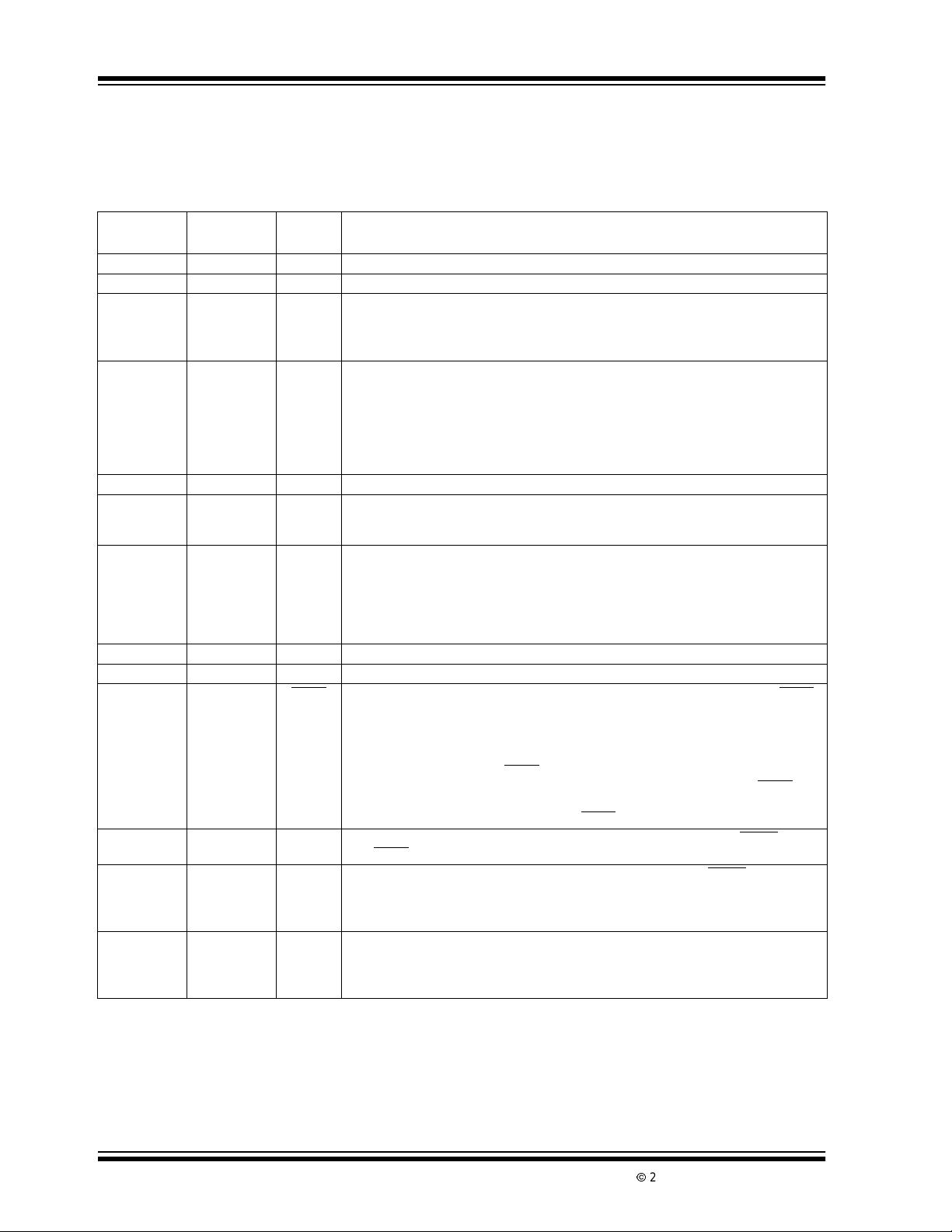
FIGURE 4-3: Typical System Application
TC520A
+5V
C
VIN+
VIN-
100k
MCP1525
1µF
10k
INT
C
AZ
R
INT
.01µ
Analog Ground
.01µ
1
INT
3
CAZ
4
BUF
11
IN+
10
IN–
9
REF+
8
REF–
5
COM
FIGURE 4-4: TC520A timing d ia gram
Read Timing
T
READ
D
OUT
D
CLK
T
RD
T
DRS
RS
T
PWL
TC500
LOAD
D
IN
D
CLK
V+
CMPTR
CR–
CR+
GND
T
DLS
16
14
13
B
12
A
6
C
7
15
2
V
-5V
DGND
Load Timing
T
LS
Crystal
REF
T
PWH
6
7
3
4
5
13
14
2
OSC
OUT
OSC
IN
CMPTR
B
TC520A
A
DV
CE
GND
LOAD
V+
LOAD
READ
D
CLK
D
IN
D
OUT
Load Default Timing
D
IN
1
12
8
10
11
9
T
LDL
T
LDS
LD
RD
SK
SO
SI
CE
DV
Read Format
Load Format
READ
READ
D
OUT
D
CLK
LOAD
D
IN
D
CLK
OVR
MSB
POL
MSB
LSB
LSB
2002 Microchip TechnologyInc. DS21431B-page 9
Page 10

TC520A
5.0 PACKAGING INFORMATION
5.1 Package Marking Information
Package marking information not availableat this time.
5.2 Taping Forms
Component Taping Orientation for 16-Pin SOIC (Wide) Devices
PIN 1
Standard Reel Component Orientation
for TR Suffix Device
Carrier Tape, Number of Components Per Reel and Reel Size
Package Carrier Width (W) Pitch (P) Part Per Full Reel Reel Size
16-Pin SOIC (W) 16 mm 12 mm 1000 13 in
User Direction of Feed
W
P
DS21431B-page 10
2002 Microchip TechnologyInc.
Page 11

5.3 Package Dimensions
)
TC520A
14-Pin PDIP (Narrow)
.770 (19.56)
.745 (18.92)
.200 (5.08)
.140 (3.56)
.150 (3.81)
.115 (2.92)
.110 (2.79)
.090 (2.29)
.070 (1.78)
.045 (1.14)
16-Pin SOIC (Wide)
.022 (0.56)
.015 (0.38)
PIN 1
.260 (6.60)
.240 (6.10)
.040 (1.02)
.020 (0.51)
.015 (0.38)
.008 (0.20)
.310 (7.87)
.290 (7.37)
3
˚
MIN.
.400 (10.16)
.310 (7.87)
Dimensions: inches (mm
.413 (10.49)
.398 (10.10)
.050 (1.27) TYP.
.019 (0.48)
.014 (0.36)
.299 (7.59)
.291 (7.40)
.012 (0.30)
.004 (0.10)
PIN 1
.419 (10.65)
.398 (10.10)
.104 (2.64)
.097 (2.46)
8°
MAX.
.050 (1.27)
.016 (0.40)
.013 (0.33)
.009 (0.23)
Dimensions: inches (mm)
2002 Microchip TechnologyInc. DS21431B-page 11
Page 12

TC520A
DS21431B-page 12
2002 Microchip TechnologyInc.
Page 13

TC520A
SALES AND SUPPORT
Data Sheets
Products supportedby a preliminaryData Sheet may have an erratasheetdescribingminor operationaldifferences and recommendedworkarounds.To determine if an erratasheetexists for a particulardevice, please contactone of the following:
1. Your local Microchip sales office
2. TheMicrochip Corporate Literature Center U.S. FAX:(480)792-7277
3. The Microchip Worldwide Site (www.microchip.com)
Pleasespecify which device, revision of silicon and Data Sheet (includeLiterature #) you are using.
New Customer Notification System
Register on our web site (www.microchip.com/cn) to receive the most currentinformationon our products.
2002 Microchip Technology Inc. DS21431B-page13
Page 14

TC520A
NOTES:
DS21431B-page 14 2002 Microchip Technology Inc.
Page 15

TC520A
Information contained in this publication regarding device
applications and the like is intended through suggestion only
and may be superseded by updates. It is your responsibility to
ensure that your application meets with your specifications.
No representation or warranty is given and no liability is
assumed by Microchip Technology Incorporated with respect
to the accuracy or use of such information, or infringementof
patents or other intellectual property rights arising from such
use or otherwise. Use of Microchip’s products as critical components in life support systems is not authorized except with
express written approval by Microchip. No licenses are conveyed, implicitly or otherwise, under any intellectual property
rights.
Trademarks
The Microchip name and logo, the Microchip logo, FilterLab,
K
EELOQ,microID,MPLAB,PIC,PICmicro,PICMASTER,
PICSTART, PRO MA TE, SEEVAL and The Embedded Control
SolutionsCompany areregiste red trademarksof MicrochipTechnologyIncorp or ated in the U.S.A. and other countries .
dsPIC, ECONOMONITOR, F anSense, FlexROM, fuzzyLA B,
In-Circuit Serial Programming, ICSP, ICEPIC, microPort,
Migratable Memory, MPASM, MPLIB, MPLINK, MPSIM,
MXDEV, PICC, PICDEM, PICDEM.net, rfPIC, Selec t M ode
and TotalEndurancearetrademarksofMicrochipTechnology
Incorporated in the U.S.A.
Serialized Quick Turn Programming (SQTP) is a service mark
of Microchip TechnologyIncorporated in t he U.S.A.
All other trademarks mentioned herein are property of their
respective companies.
© 2002, Microchip T echnology Incorporated, Printed in the
U.S.A., All Rights Reserved.
Printed on recycled paper.
Microchip received QS-9000 quality system
certification for its worldwide headquarters,
design and wafer fabrication facilities in
Chandler and Tempe, Arizona in July 1999
and Mountain View, California in March 2002.
The Company’s quality system processes and
procedures are QS-9000 compliant for its
®
PICmicro
devices, Serial EEPROMs, microperipherals,
non-volatile memory and analog products. In
addition, Microchip’s quality system for the
design and manufacture of development
systemsisISO 9001certified.
2002 Microchip TechnologyInc. DS21431B-page 15
8-bit MCUs, KEELOQ®code hopping
Page 16

WORLDWIDE SALES AND SERVICE
AMERICAS
Corporate Office
2355 West Chandler Blvd.
Chandler, AZ 85224-6199
Tel: 480-792-7200 Fax: 480-792-7277
Technical Support: 480-792-7627
Web Address: http://www.microchip.com
Rocky Mountain
2355 West Chandler Blvd.
Chandler, AZ 85224-6199
Tel: 480-792-7966 Fax: 480-792-7456
Atlanta
500 Sugar Mill Road, Suite 200B
Atlanta, GA 30350
Tel: 770-640-0034 Fax: 770-640-0307
Boston
2 Lan Drive, Suite 120
Westford, MA 01886
Tel: 978-692-3848 Fax: 978-692-3821
Chicago
333 Pierce Road, Suite 180
Itasca, IL 60143
Tel: 630-285-0071 Fax: 630-285-0075
Dallas
4570 Westgrove Drive, Suite 160
Addison, TX 75001
Tel: 972-818-7423 Fax: 972-818-2924
Detroit
Tri-Atria Office Building
32255 Northwestern Highway, Suite 190
Farmington Hills, MI 48334
Tel: 248-538-2250 Fax: 248-538-2260
Kokomo
2767 S. Albright Road
Kokomo, Indiana 46902
Tel: 765-864-8360 Fax: 765-864-8387
Los Angeles
18201 Von Karman, Suite 1090
Irvine, CA 92612
Tel: 949-263-1888 Fax: 949-263-1338
New York
150 Motor Parkway, Suite 202
Hauppauge, NY 11788
Tel: 631-273-5305 Fax: 631-273-5335
San Jose
Microchip Technology Inc.
2107 North First Street, Suite 590
San Jose, CA 95131
Tel: 408-436-7950 Fax: 408-436-7955
Toronto
6285 Northam Drive, Suite 108
Mississauga, Ontario L4V 1X5, Canada
Tel: 905-673-0699 Fax: 905-673-6509
ASIA/PACIFIC
Australia
Microchip Technology Australia Pty Ltd
Suite 22, 41 Rawson Street
Epping 2121, NSW
Australia
Tel: 61-2-9868-6733 Fax: 61-2-9868-6755
China - Beijing
Microchip Technology Consulting (Shanghai)
Co., Ltd., Beijing Liaison Office
Unit 915
Bei Hai Wan Tai Bldg.
No. 6 Chaoyangmen Beidajie
Beijing, 100027, No. China
Tel: 86-10-85282100 Fax: 86-10-85282104
China - Chengdu
Microchip Technology Consulting (Shanghai)
Co., Ltd., Chengdu Liaison Office
Rm. 2401, 24th Floor,
Ming Xing Financial Tower
No. 88 TIDU Street
Chengdu 610016, China
Tel: 86-28-86766200 Fax: 86-28-86766599
China - Fuzhou
Microchip Technology Consulting (Shanghai)
Co., Ltd., Fuzhou Liaison Office
Unit 28F, World Trade Plaza
No. 71 Wusi Road
Fuzhou 350001, China
Tel: 86-591-7503506 Fax: 86-591-7503521
China - Shanghai
Microchip Technology Consulting (Shanghai)
Co., Ltd.
Room 701, Bldg. B
Far East International Plaza
No. 317 Xian Xia Road
Shanghai, 200051
Tel: 86-21-6275-5700 Fax: 86-21-6275-5060
China - Shenzhen
Microchip Technology Consulting (Shanghai)
Co., Ltd., Shenzhen Liaison Office
Rm. 1315, 13/F , Shenzhen Kerry Centre,
Renminnan Lu
Shenzhen 518001, China
Tel: 86-755-2350361 Fax: 86-755-2366086
China - Hong Kong SAR
Microchip Technology Hongkong Ltd.
Unit 901-6, T ower2, Metroplaza
223 Hing Fong Road
Kwai Fong, N.T ., Hong Kong
Tel: 852-2401-1200 Fax: 852-2401-3431
India
Microchip Technology Inc.
India Liaison Office
Divyasree Chambers
1 Floor, Wing A (A3/A4)
No. 11, O’Shaugnessey Road
Bangalore, 560 025, India
Tel: 91-80-2290061 Fax: 91-80-2290062
Japan
Microchip Technology Japan K.K.
Benex S-1 6F
3-18-20, Shinyokohama
Kohoku-Ku, Yokohama-shi
Kanagawa, 222-0033, Japan
Tel: 81-45-471- 6166 Fax: 81-45-471-6122
Korea
Microchip Technology Korea
168-1, Youngbo Bldg. 3 Floor
Samsung-Dong, Kangnam-Ku
Seoul, Korea 135-882
Tel: 82-2-554-7200 Fax: 82-2-558-5934
Singapore
Microchip Technology Singapore Pte Ltd.
200 Middle Road
#07-02 Prime Centre
Singapore, 188980
Tel: 65-6334-8870 Fax: 65-6334-8850
Taiwan
Microchip Technology Taiwan
11F-3, No. 207
Tung HuaNorth Road
Taipei, 105, T aiwan
Tel: 886-2-2717-7175 Fax: 886-2-2545-0139
EUROPE
Denmark
Microchip Technology Nordic ApS
Regus Business Centre
Lautrup hoj 1-3
Ballerup DK-2750 Denmark
Tel: 45 4420 9895 Fax: 45 4420 9910
France
Microchip Technology SARL
Parc d’Activite du Moulin de Massy
43 Rue du Saule Trapu
Batiment A - ler Etage
91300 Massy, France
Tel: 33-1-69-53-63-20 Fax: 33-1-69-30-90-79
Germany
Microchip Technology GmbH
Gustav-Heinemann Ring 125
D-81739 Munich, Germany
Tel: 49-89-627-144 0 Fax: 49-89-627-144-44
Italy
Microchip Technology SRL
Centro Direzionale Colleoni
Palazzo Taurus 1 V. Le Colleoni 1
20041 Agrate Brianza
Milan, Italy
Tel: 39-039-65791-1 Fax: 39-039-6899883
United Kingdom
Microchip Ltd.
505 Eskdale Road
Winnersh Triangle
Wokingham
Berkshire, EnglandRG41 5TU
Tel: 44 118 921 5869 Fax: 44-118 921-5820
04/20/02
DS21431B-page 16
*DS21431B*
2002 Microchip Technology Inc.
 Loading...