

Datasheet TC500CPE, TC500COE, TC500ACPE, TC500ACOE, TC510CPF Datasheet (Microchip Technology)
...Page 1
TC500/A/510/514
Precision Analog Front Ends
Features
• Precision (up to 17-bits) A/D Converter "Front End"
• 3-Pin Control Interface to Microprocessor
• Flexible: User Can Trade-off Conversion Speed
for Resolution
• Single Supply Operation (TC510/TC514)
• 4 Input, Differential Analog MUX (TC514)
• Automatic Input Voltage Polarity Detection
• Low Power Dissipation:
- (TC500/TC500A):10mΩ
- (TC510/TC514):18mΩ
• Wide Analog Input Range: ±4.2V (TC500A/TC510)
• Directly Accepts Bipolar and Differential
Input Signals
Applications
• Precision Analog Signal Processor
• PrecisionSensor Interface
• High Accuracy DC Measurements
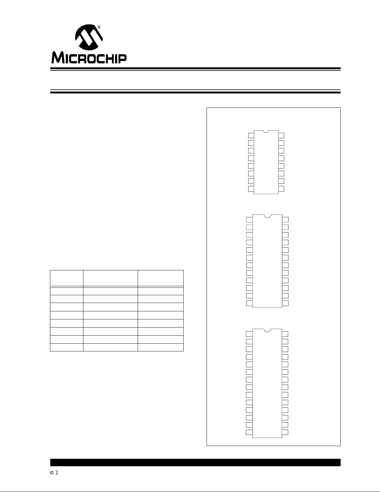
Device Selection Table
Part
Number
Package
TC500ACOE 16-Pin SOIC (Wide) 0°C to +70°C
TC500ACPE 16-Pin PDIP (Narrow) 0°C to +70°C
TC500COE 16-Pin SOIC (Wide) 0°C to +70°C
TC500CPE 16-Pin PDIP (Narrow) 0°C to +70°C
TC510COG 24-Pin SOIC (Wide) 0°C to +70°C
TC510CPF 24-Pin PDIP (Narrow) 0°C to +70°C
TC514COI 28-Pin SOIC (Wide) 0°C to +70°C
TC514CPJ 28-Pin PDIP (Narrow) 0°C to +70°C
Temperature
Range
Package Types
1
C
INT
V
2
SS
C
3
AZ
4
BUF
ACOM
5
C
–
6
REF
C
+
7
REF
V
8
REF
-
V
1
OUT
C
2
INT
C
3
AZ
BUF
4
ACOM
C
V
ACOM
C
V
C
REF
REF
REF
V
REF
V
OUT
C
C
REF
REF
V
REF
REF
CH4-
CH3-
CH2-
CH1-
N/C
N/C
N/C
INT
C
AZ
BUF
N/C
5
-
6
7
+
8
+
9
-
10
11
12
-
1
2
3
4
5
6
-
+
7
-
8
+
9
10
11
12
13
14
16-Pin SOIC
16 Pin-PDIP
TC500/
TC500A
COE
TC500/
TC500A
CPE
24-Pin SOIC
24-Pin PDIP
TC510COG
TC510CPF
28-Pin SOIC
28-Pin PDIP
TC514COI
TC514CPJ
V
16
DD
15
DGND
14
CMPTR OUT
13
B
A
12
VIN+
11
V
10
IN
V
9
REF
24
CAP-
23
DGND
22
CAP+
21
V
20
OSC
19
CMPTR OUT
18
A
17
B
16
V
15
V
14
N/C
13
N/C
28
CAP-
27
DGND
26
CAP+
V
25
24
OSC
23
CMPTR OUT
22
A
21
B
20
A0
19
A1
18
CH1+
17
CH2+
16
CH3+
CH4+
15
–
DD
IN
IN
DD
+
+
-
2002 Microchip TechnologyInc. DS21428B-page 1
Page 2
TC500/A/510/514
)
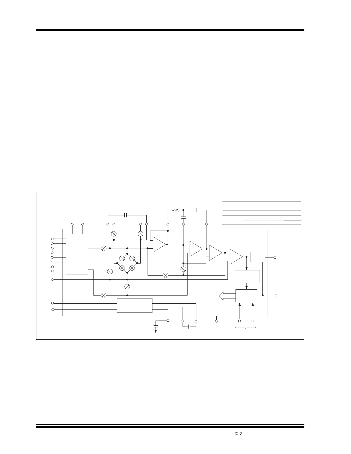
General Description
TheTC500/A/510/514 family are precision analog front
ends that implement dual slope A/D converters having
a maximum resolution of 17-bits plus sign. As a minimum, each device contains the integrator, zero crossing comparator and processor i nterface logic. The
TC500 is the base (16-bit max) device and requires
both positive and negative power supplies. The
TC500A is identical to t he TC500 with the exception
that it has improved linearity, allowing it to operate to a
maximumresolutionof17-bits.The TC510 adds an onboard negative power supply converter for single supply operation. The TC514 adds both a negative power
supply converter and a 4 input differential analog
multiplexer.
Each device has the same processor control interface
consistingof3 wires: control inputs(A and B)and zerocrossing comparator output (CMPTR). The processor
manipulates A, B to sequence the TC5XX through four
phases of conversion: Auto Zero, Integrate, De-integrate and IntegratorZero. During the Auto Zero phase,
Typical Application
C
REF
V
REF
SW
R
-
SW
RI
-
SW
RI
SW
1
DC-TO-DC
Converter
C
REF
Buffer
-
+
CH1+
CH2+
CH3+
CH4+
CH1CH2CH3CH4-
ACOM
V
OSC
+
A1
A0
DIF.
MUX
(TC514)
SS
V
REF
SW
SW
SW
+
I
Z
I
REF
SW
R
SW
-
RI
SWRI+
(TC510 & TC514)
C
-
SW
offset voltages in the TC5XX are corrected by a closed
loop feedback mechanism.The input voltage is applied
to the integrator during the I ntegrate phase. This
causes an integrator output dv/dt directly proportional
to the magnitude of the input voltage. The higher the
input voltage, the greater the magnitude of the voltage
stored on the integrator during this phase. At the start
of the De-integrate phase, an external voltage reference is applied to the integratorand, at the same time,
the external host processor starts i ts on-board timer.
The processor maintains t his state until a transition
occurson the CMPTR output,atwhichtimetheprocessor halts its timer. The resultingtimer count is the converted analog data. Integrator Zero (the final phase of
conversion) removes any residue remaining in the
integrator in preparationfor the next conversion.
The TC500/A/510/514 offer high resolution (up to 17bits), superior 50Hz/60Hz noise r ejection, low power
operation, minimum I/O connections, low input bias
currents and lower cost compared to other converter
technologies having similarconversion speeds.
Control Logic
TC500
TC500A
TC510
TC514
Polarity
Detection
Phase
Decoding
Logic
Converter Sate
Level
Shift
R
INT
C
BUF
SW
IZ
V
OUT
C
INT
AZ
C
AZ
Integrator
–
+
Z
Analog
Switch
Control
Signals
CAP-
CAP+
A B
0 0 Zero Integrator Output
0 1 Auto-Zero
1 0 Signal Integrate
1 1 Deintegrate
C
INT
CMPTR 1
+
–
CMPTR 2
–
+
CMPTR
Output
DGND
DS21428B-page 2
1.0µF
V
SS
C
-
OUT
1.0µF
(TC500
TC500A
BA
Control Logic
2002 Microchip TechnologyInc.
Page 3
TC500/A/510/514
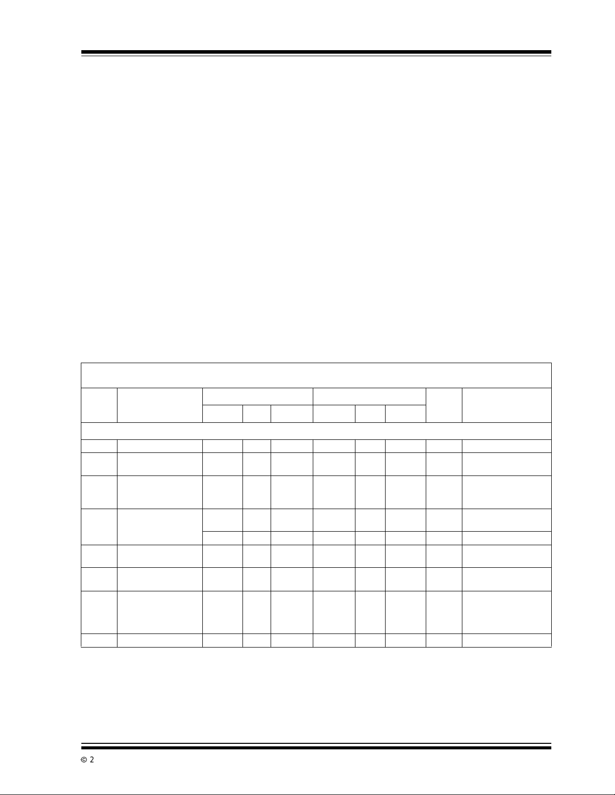
1.0 ELECTRICAL
CHARACTERISTICS
Absolute Maximum Ratings*
TC510/TC514 Positive Supply Voltage
(V
to GND) .........................................+10.5V
DD
TC500/TC500A Supply Voltage
(V
to VSS) ..............................................+18V
DD
TC500/TC500A Positive Supply Voltage
(V
to GND) ............................................+12V
DD
TC500/TC500A Negative Supply Voltage
(V
to GND)................................................-8V
SS
Analog Input Voltage(V
Logic Input Voltage...............VDD+0.3Vto GND - 0.3V
Voltage on OSC:
........................... -0.3V to (V
Ambient Operating Temperature Range:
................................................................0°C to +70°C
StorageTemperature Range: .............-65°C to +150°C
TC500/A/510/514 ELE CTRI CAL SPECIFICATIONS
+orVIN-) ............VDDto V
IN
+0.3V)for VDD<5.5V
DD
SS
*Stresses above those listed under "Absolute Maximum Ratings" may cause permanent damage to t he
device. These are stress ratings only and functional
operation of the device at these or any other conditions
above those indicated in the operation sections of the
specifications is not implied. Exposure to Absolute
Maximum Rating conditions for extended periods may
affect device reliability.
Electrical Characteristics: TC510/TC514: VDD= +5V, TC500/TC500A: VSS= ±5V unless otherwise specified.
C
AZ=CREF
Symbol Parameter
Analog
ZSE Zero Scale Error
ENL End Point Linearity ——0.005—0.015
NL Best Case Straight
ZS
TC
SYE Full-Scale Symmetry
FS
TC
I
IN
Note 1: Integrate time ≥ 66msec, auto zero time ≥ 66msec, V
=0.47µF.
=+25°C TA=0°Cto70°C
T
A
Min Typ Max Min Typ Max
Resolution 60 — — — —— µVNote1
—
with Auto Zero Phase
Line Linearity
Zero-Scale Temp.
Coefficient
Error (Roll-Over Error)
Full-Scale Tempera-
ture Coefficient
Input Current — 6 — — —— pAVIN=0V
2: End point linearity at ±1/4, ±1 /2, ±3/4 F.S. after full-scale adjustment.
3: Roll-overerrorisrelated to C
—
— 0.003 0.008 —
— — 0.005 — — — % F.S. TC500A
——— — 12µV/°C Over Operating
—0.01— — 0.03 — % F.S. Note 3
——— — 10 — ppm/°C Over Operating
—
—
INT,CREF,CAZ
0.005
0.003
0.010
(peak) ≈ 4V.
INT
characteristics.
—
—
—
—
0.005
0.003
0.015
0.010
0.012
0.009
0.060
0.045
— — % F.S. TC500/510/514,
Unit Test Conditions
% F.S. TC500/510/514
TC500A
%F.S.
%F.S.
TC500/510/514,
Note 1, Note 2,
TC500A
Note 1, Note 2
Temperature Range
Temperature Range;
External Reference
TC = 0 ppm/°C
2002 Microchip TechnologyInc. DS21428B-page 3
Page 4
TC500/A/510/514
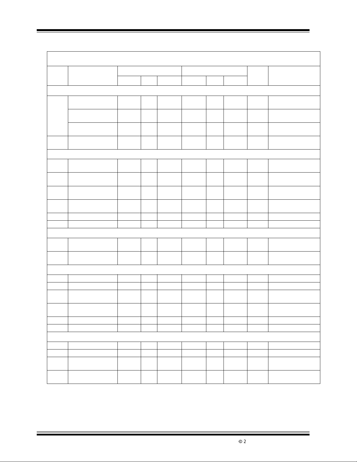
TC500/A/510/514 ELE CTRICAL SPECIFICATIONS (CONTINUED)
Electrical Characteristics: TC510/TC514: VDD= +5V, TC500/TC500A: VSS= ±5V unless otherwise specified.
C
AZ=CREF
Symbol Parameter
Analog (Continued)
V
CMR
V
REF
Digital
V
OH
V
OL
V
IH
V
IL
I
L
t
D
Multiplexer (TC514 Only)
R
DSON
Power (TC510/TC514 Only)
I
S
P
D
V
DD
R
OUT
I
OUT
Power (TC500/TC500A Only)
I
S
P
D
V
DD
V
SS
Note 1: Integrate time ≥ 66msec, auto zero time ≥ 66msec, V
=0.47µF.
=+25°C TA=0°Cto70°C
T
A
Min Typ Max Min Typ Max
Common Mode
VSS+1.5 — VDD–1.5 VSS+1.5 — VDD–1.5 V
Voltage Range
Integrator Output
+0.9 — VDD–0.9 VSS+0.9 — VSS+0.9 V
V
SS
Swing
Analog Input Signal-
+1.5 — VDD–1.5 VSS+1.5 — VSS+1.5 V ACOM= GND = 0V
V
SS
Range
Voltage Reference
VSS+1 — VDD–1 VSS+1 — VDD–1 V V
Range
Comparator Logic 1,
4 — —4——VI
Output High
Comparator Logic 0,
— — 0.4 — — 0.4 V I
OutputLow
Logic1, InputHigh
3.5 — —3.5——V
Voltage
Logic0, InputLow
— — 1——1V
Voltage
LogicInputCurrent — — ——0.3 µALogic1or0
Comparator Delay — 2 — — 3 — µsec
Maximum Input
-2.5 — 2.5 -2.5 — 2.5 V V
Voltage
Drain/Source ON
—610 ———kΩ VDD=5V
Resistance
SupplyCurrent — 1.8 2.4 — — 3.5 mA VDD=5V,A=1,B=1
Power Dissipation — 18 — — — — mW VDD=5V
Positive Supply Oper-
4.5 — 5.5 4.5 — 5.5 V
ating Voltage Range
Operating Source
—6085 — —100Ω I
Resistance
Oscillator Frequency — 100 — — — — kHz (Note3)
Maximum Current Out — — -10 — — -10 mA VDD=5V
Supply Current — 1 1.5 — — 2.5 mA VS=±5V,A=B=1
Power Dissipation — 10 — — — — mW VDD=5V,VSS=-5V
Positive Supply Oper-
4.5 — 7.5 4.5 — 7.5 V
ating Range
Negative Supply
-4.5 — -7.5 - 4.5 — -7.5 V
Operating Range
(peak) ≈ 4V.
2: End point linearity at ±1/4, ±1 /2, ±3/4 F.S. after full-scale adjustment.
3: Roll-overerrorisrelated to C
INT,CREF,CAZ
characteristics.
INT
Unit Test Conditions
REF-VREF
SOURCE
SINK
DD
OUT
+
=400µA
=2.1mA
=5V
=10mA
DS21428B-page 4
2002 Microchip TechnologyInc.
Page 5
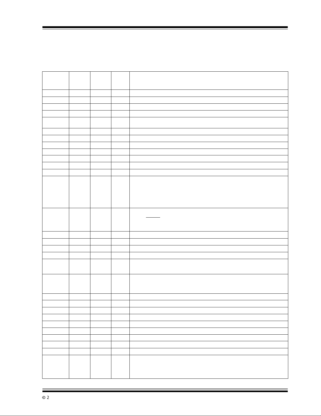
2.0 PIN DESCRIPTIONS
ThedescriptionsofthepinsarelistedinTable2-1.
TABLE 2-1: PIN FUNCTION TABLE
TC500/A/510/514
PinNumber
(TC500,
TC500A)
122C
2 Not Used Not Used V
333C
Pin
Number
(TC510)
Pin
Number
(TC514)
Symbol Description
Integrator output. Integrator capacitor connection.
INT
Negative power supply input(TC500/TC500A only).
SS
Auto Zero input. The Auto Zero capacitor connection.
AZ
4 4 4 BUF Buffer output. The Integrator capacitor connection.
5 5 5 ACOM This pin is grounded in most applications. It is recommended that ACOM and the
666C
777C
888V
999V
10 15 Not Used V
11 16 Not Used V
input common pin (Ve
- Input.Negative reference capacitor connection.
REF
+ Input. Positive reference capacitor connection.
REF
- Input. External voltage reference (-) connection.
REF
+ Input. External voltage reference (+) connection.
REF
- Negative analog input.
IN
+ Positive analog input.
IN
-orCHn-) be within the analog common mode range (CMR).
n
12 18 22 A Input. Converter phase control MSB. (See input B.)
13 17 21 B Input. Converter phase control LSB. The states of A, B place the TC5XX in one of
four required phases. A conversion is complete when all four phases have been
executed:
Phasecontrol input pins: AB = 00: IntegratorZero
01: Auto Zero
10: Integrate
11: De-integrate
14 19 23 CMPTR
Zerocrossing comparatoroutput. CMPTR is HIGH during the Integration phase
OUT
when a positive
voltage is being integrated. A HIGH-to-LOW transition on CMPTR signals the processorthat the De-integrate phase is completed. CMPTR is undefinedduring the
AutoZerophase.Itshouldbe monitored to time theIntegrator Zero phase.
input voltage is being integratedand is LOW when a negative input
15 23 27 DGND Input. Digital ground.
16 21 25 V
Input.Power supply positive connection.
DD
22 26 CAP+ Input. Negative power supply converter capacitor (+) connection.
24 28 CAP- Input. Negative power supply converter capacitor (-) connection.
11V
- Output. Negative power supply converter output and reservoir capacitor connection.
OUT
This output can be used to power other devices in the circuit requiringa negative
biasvoltage.
20 24 OSC Oscillator control input. The negative powersupplyconverter normally runs at a fre-
quency of 100kHz. The converter oscillator frequencycanbe sloweddown
(to reduce quiescent current) by connecting an external capacitor between this pin
and V
(see Section9.0, Typical Characteristics Curves).
DD
18 CH1+ Positiveanalog input pin. MUX channel 1.
13 CH1- Negative analog input pin. MUX channel 1.
17 CH2+ Positiveanalog input pin. MUX channel 2.
12 CH2- Negative analog input pin. MUX channel 2.
16 CH3+ Positiveanalog input pin. MUX channel 3.
11 CH3- Negative analog inputpin. MUX channel3.
15 CH4+ Positiveanalog input pin. MUX channel 4.
10 CH4- Negative analog input pin. MUX channel 4
20 A0 Multiplexer inputchannel select input LSB (see A1).
19 A1 Multiplexer input channel select input MSB.
Phasecontrol input pins: A1, A0 = 00 = Channel1
01 = Channel 2
10 = Channel 3
11 = Channel4
2002 Microchip TechnologyInc. DS21428B-page 5
Page 6
TC500/A/510/514
T
3.0 DETAILED DESCRIPTION
3.1 Dual Slope Conversion Principles
Actual data conversion is accomplishedin t wo phases:
input signal Integrationand reference voltage
De-integration.
The integratoroutputisinitializedt o 0Vprior to the start
of Integration. During Integration, analog switch S1
connects V
tained for a fixed time period (T
V
causes t he integrator output to depart 0V at a rate
IN
determined by the magnitude of V
determined by the polarity of V
phase is initiated immediately at the expiration of T
DuringDe-integration, S1 connectsa reference voltage
(having a polarity opposite that of V
input. At the same time, an external precision timer i s
started. The De-integration phase is maintained until
the comparator output changes state, indicating the
integratorhas returned to its starting point of 0V. When
thisoccurs,the precisiontimerisstopped.TheDe-integration time period (T
sion timer, is directly proportional to the magnitude of
the applied input voltage (see Figure 3-3).
A simple mathematical equation relates the Input Signal, Reference Voltage and Integration time:
EQUATION 3-1:
Where:
V
= Reference Voltage
REF
= Signal Integration time (fixed)
T
INT
t
DEINT
For a constant VIN:
EQUATION 3-2:
The dual slope converter accuracy is unrelated to the
integrating resistor and capacitor values as long as
they are stable during a measurement cycle.
An inherent benefit is noise immunity. Input noise
spikes are i ntegrated (averaged to zero) during the
integration periods. Integrating ADCs are immune to
the large conversion errors that plague successive
approximation converters in high noise environments.
Integrating converters provide inherent noise rejection
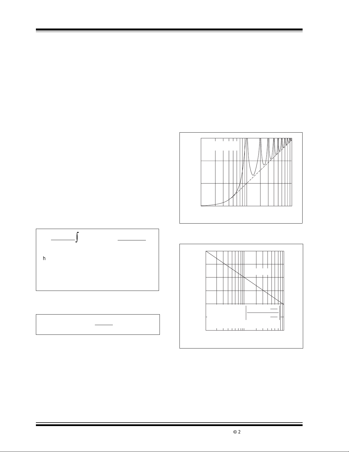
with at least a 20dB/decade attenuation rate. Interference signals with frequencies at integral multiples of
to the integrator input where it is main-
R
INTCINT
IN
),as measured by the preci-
DEINT
T
1
INT
∫
V
IN
0
). The application of
INT
and a direction
IN
. The De-integration
IN
) to the integrator
IN
V
(T)DT =
REFTDEINT
R
INT
INTCINT
= Reference Voltage Integrationtime(variable)
T
REF
DEINT
T
INT
VIN=V
the integration period are, theoretically, completely
removed, since the average value of a sine wave of
frequency (1/T) averaged over a period (T) is zero.
Integrating converters often establish the integration
period to reject 50/60Hz line frequency interference
signals. The abilityto reject such signals is shown by a
normal mode rejection plot (Figure 3-1). Normal mode
rejection is limited in practice to 50 to 65dB, since the
line frequency can deviate by a few tenths of a percent
(Figure3-2).
FIGURE 3-1: INTEGRATING
CONVERTER NORMAL
.
30
Measurment
T =
Period
20
10
Normal Mode Rejection (dB)
0
0.1/T 1/T 10/
MODE REJECTION
Input Frequency
FIGURE 3-2: LINE FREQUENCY
DEVIATION
80
70
60
t = 0.1 sec
50
40
Normal Mode
REJECTION
30
DEV = Deviation from 60Hz
Normal Mode Rejeciton (dB)
t = Integration Period
20
= 20 LOG
SIN 60 t (1 ± )
0.01 0.1
DEV
p
100
DEV
p
60 t (1 ± )
100
1.0
Line Frequency Deviation from 60 Hz (%)
DS21428B-page 6
2002 Microchip TechnologyInc.
Page 7
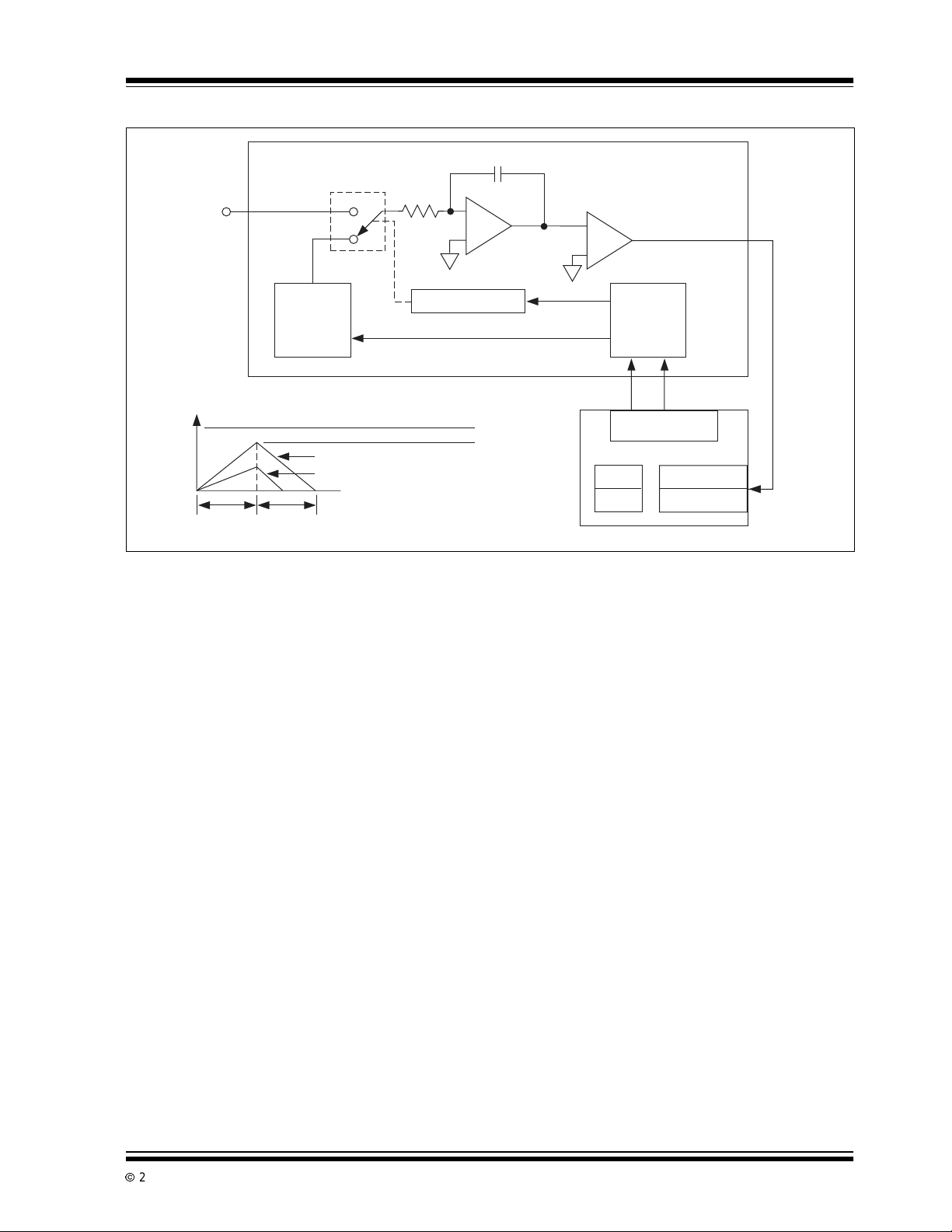
FIGURE 3-3: BASIC DUAL SLOPE CONVERTER
C
INT
Analog
Input (V
R
INT
)
IN
S1
Integrator
–
+
±
REF
VOLTAGE
Switch Driver
Polarity Control
TC500/A/510/514
TC510
V
INT
Phase
Control
–
+
Comparator
Control
Logic
AB
CMPTR Out
Output
Integrator
T
INT
T
DEINT
V
V
IN
IN
≈ V
REF
≈ 1/2 V
REF
V
SUPPLY
V
INT
Microcomputer
ROM
RAM
I/O
Timer
Counter
2002 Microchip TechnologyInc. DS21428B-page 7
Page 8
TC500/A/510/514
4.0 TC500/A/510/514 CONVERTER
OPERATION
The TC500/A/510/514 incorporates an Auto Zero and
IntegratorphaseinadditiontotheinputsignalIntegrate
and reference De-integrate phases. The addition of
these phases reduce system errors, calibration steps
and shorten overrange recovery time. A typical measurement cycle uses all four phases in the following
order:
1. Auto Zero
2. Input signal integration
3. Reference deintegration
4. Integrator output zero
The internal analog switch status for each of these
phases is summarized in Table 4-1. This table
references the Typical Application.
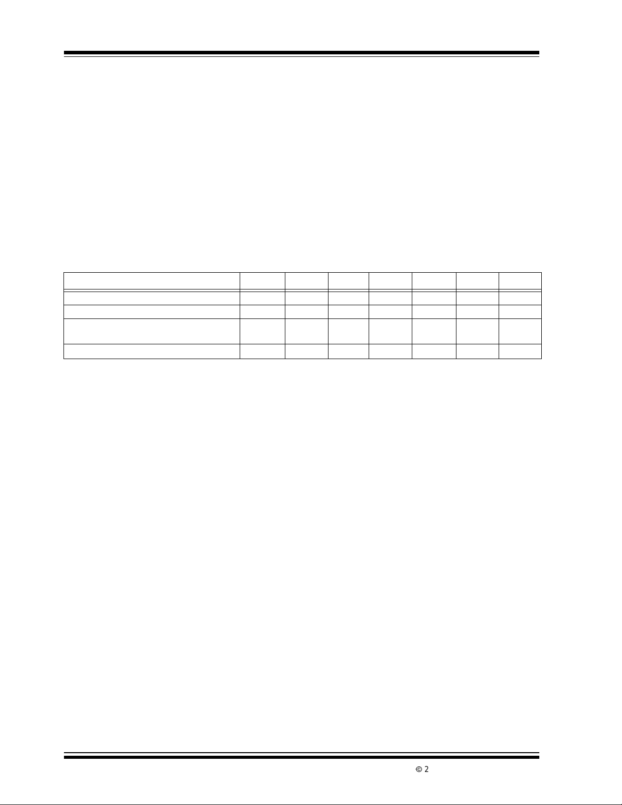
TABLE 4-1: INTERNAL ANALOG GATE STATUS
Conversion Phase SW
Auto Zero (A = 0, B = 1) Closed Closed Closed
Input Signal Integration (A = 1, B = 0) Closed
Reference Voltage De-integration
(A =1, B = 1)
Integrator Output Zero (A = 0, B = 0) Closed Closed Closed
Note: *Assumes a positive polarity input signal. SW
SWR+SWR-SWZSW
I
Closed* Closed
–
would be closed for a negative i nput signal.
RI
R
SW
SW
1
IZ
4.1 Auto Zero Phase (AZ)
During this phase, errors due to buffer, integrator and
comparator offset voltages are nulled out by charging
C
(auto zero capacitor) with a compensating er ror
AZ
voltage.
The externalinputsignal is disconnectedfromtheinter-
nal circuitry by opening the two SW
internal input points connect to analog common. The
referencecapacitoris charged to the reference voltage
potentialthroughSW
the integrator and comparator, charges the C
itor with a voltage to compensate for buffer amplifier,
integrator and comparator offset voltages.
.A feedbackloop,closedaround
R
switches. The
I
capac-
AZ
4.2 Analog Input Signal Integration
Phase (INT)
The TC5XX integratesthe differential voltage between
the (V
must be within the device's Common mode range
V
software at the end of this phase: CMPTR = 1 for
positive polarity; CMPTR = 0 for negative polarity.
+) and (VIN–) inputs. The differential voltage
IN
. The input signal polarityisnormally checked via
CMR
4.3 Reference Voltage De-integration
Phase (D
The previously charged reference capacitor is connected with the proper polarity to ramp the integrator
output back to zero. An externally-provided, precision
timer is used to measure the duration of this phase.
The resulting time measurement is proportional to the
magnitude of the applied input voltage.
INT
)
4.4 Integrator Output Zero Phase (IZ)
This phase ensuresthe integrator output is at 0V when
the Auto Zero phase is entered and that only system
offsetvoltagesare compensated.Thisphaseisused at
the end of the reference voltage de-integration phase
and MUST be usedfor ALL TC5XX applicationshaving
resolutionsof 12-bits or more. If t his phase is not used,
the value of the Auto Zero capacitor (C
about 2 to 3 times thevalue of the Integrationcapacitor
(C
) to reduce the effectsofchargesharing.TheInte-
INT
grator Output Zero phase should be programmed to
operate until the output of the comparator returns
"HIGH". The overall timing system is shown in
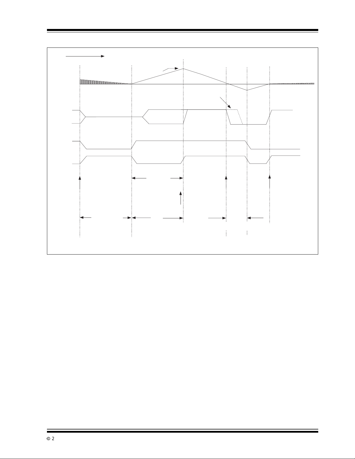
Figure 4-1.
)mustbe
AZ
DS21428B-page 8
2002 Microchip TechnologyInc.
Page 9
TC500/A/510/514
FIGURE 4-1: TYPICAL DUAL SLOPE A/D CONVERTER SYSTEM TIMING
T
TIME
Converter Status
Integrator
Voltage
V
INT
Auto-Zero
0
Integrate
Full Scale Input
Reference
De-integrate
Comparator Delay
Overshoot Integrator
Output
Zero
Comparator
Output
A
AB Inputs
B
Controller
Operation
Notes:
Undefined
A = 0
B = 1
Begin Conversion with
Auto-Zero Phase
Typically = T
(Positive Input Shown)
The length of this phase is chosen almost arbitrarily
but needs to be long enough to null out worst case errors
(see text).
INT
0 For Negative Input
1 For Postive Input
A = 1
B = 0
Time Input
Integration
Phase
Sample Input Polarity
T
INT
Capture
De-integration
Time
A = 1
B = 1
A = 0
B = 0
I
ntegrator
Output
Zero Phase
Complete
Comparator Delay +
Processor Latency
Ready for Next
Conversion
(Auto-Zero is
Idle State)
Minimizing
Overshoot
will Minimize
I.O.Z. Time
2002 Microchip TechnologyInc. DS21428B-page 9
Page 10

TC500/A/510/514
5.0 ANALOG SECTION
5.1 Differential Inputs (V
The TC5XX operates with differential voltages within
the input amplifierCommon mode range. The amplifier
Common mode range extends from 1.5V below positive supply to 1.5V above negative supply. Within this
Common mode voltage range, C ommon mode rejectionis typically 80dB. Full accuracy is maintained,however,when the inputsare no less than 1.5V from either
supply.
The integrator output also follows t he Common mode
voltage. The integrator output must not be allowed to
saturate. A worst case condition exists, for example,
when a large, positive Common mode voltage, with a
near full scale negative differential input voltage, is
applied. The negative input signal drives the integrator
positive when most of its swing has been used up by
the positive Common mode voltage. For these critical
applications,the integrator swing can be reduced. The
integratoroutput can swing within 0.9V of either supply
without loss of linearity.
5.2 Analog Common
Analog common is used as VINreturn during system
zeroandreferencede- integrate.IfV
analog common, a Common modevoltageexistsinthe
system. This signal is rejected by the excellent CMR of
the converter.Inmost applications,V
fixed known voltage ( i.e., power supply common). A
Common mode voltage will exist when V
connected to analog common.
5.3 Differential Reference
+,V
(V
REF
The reference voltage can be anywhere within 1V of
the power supply voltage of the converter. Rollover
error is caused by the reference capacitor losing or
gaining charge due t o stray capacitance on its nodes.
REF
–)
+,V
IN
IN
IN
–)
IN
– is differentfrom
–willbesetata
– is not
IN
The difference in reference for (+) or (-) input voltages
will cause a rollover error. This error can be minimized
by using a large r eference capacitor in comparison to
the stray capacitance.
5.4 P hase Control Inputs (A, B)
The A, B unlatchedlogicinputsselectthe TC5XX operating phase. The A, B inputs are normally driven by a
microprocessorI/O port or external logic.
5.5 Com parator Output
By monitoring the comparator output during the fixed
signal integrate time, the input signal polarity can be
determined by the microprocessor controlling the
conversion.Thecomparatoroutput is HIGH forpositive
signals and LOW f or negative signals during the signal
integrate phase (see Figure 5-1).
During the referencede-integratephase,the comparator output will make a HIGH-to-LOW transition as the
integrator output ramp crosses z ero. The transition is
used to signal the processor that the conversion is
complete.
The internal comparator delay is 2µsec, typically.
Figure 5-1 shows the comparator output for large
positive and negative signal inputs.For signal inputsat
or near zero volts, however,theintegratorswingis very
small.If Common mode noise is present,the comparator can switch several timesduringthe beginningof the
signal integrate period. To ensure that the polarity
reading i s correct, the comparator output should be
read and stored at the end of the signal integrate
phase.
The comparator output is undefined during the Auto
Zero phase and is used to time the Integrator Output
Zero phase. (See Section 7.6, Integrator Output Zero
Phase).
FIGURE 5-1: COMPARATOR OUTPUT
Reference
Deintegrate
Integrator
Output
Comparator
Output
DS21428B-page 10
Signal
Integrate
Zero
Crossing
Integrate
Integrator
Output
Comparator
Output
Signal
B. Negative Input SignalA. Positive Input Signal
Reference
De-integrate
Zero
Crossing
2002 Microchip TechnologyInc.
Page 11

TC500/A/510/514
6.0 TYPICAL APPLICATIONS
6.1 Component Value Selection
The pr ocedure outlined below allows the user to arrive
at values for the following TC5XX design variables:
1. Integration Phase Timing
2. Integrator Timing Components (R
INT,CINT
3. Auto Zero and Reference Capacitors
4. Voltage Reference
6.2 Select Integration Time
Integration time must be picked as a multiple of the
periodof the line frequency. For example, T
33msec, 66msec and 132msec maximize 60Hz line
rejection.
6.3 DINT and IZ Phase Timing
The duration of the D INT phase is a function of the
amount of voltage stored on the integrator during T
and the value of V
. The DI NT phase must be initi-
REF
ated immediately following INT and terminated when
an integrator output zero-crossing is detected. In general, the maximum number of counts chosen for DINT
istwicethatofINT(withV
chosen at V
REF
6.4 Calculate Integrating Resistor
)
(R
INT
The desired full scale input voltageandamplifieroutput
current capability determine the value of R
buffer and integrator amplifiers each have a full-scale
currentof20µA.
The v alue of R
following equation:
is therefore directly calculated in the
INT
)
timesof
INT
IN(MAX)
INT
INT
/2).
.The
TABLE 6-1: C
Conversions
Per Second
>7 0.1 SMR5 104K50J01L4
2 to 7 0.22 SMR5 224K50J02L4
2 or less 0.47 SMR5 474K50J04L4
Note: Manufactured by Evox-Rifa, Inc.
Typical Value of
C
AND CAZSELECTION
REF
REF,CAZ
(µF)
Suggested* Part
Number
6.6 Calculate Integrating Capacitor
)
(C
INT
The integratingcapacitor mustbe selected tomaximize
integrator output voltage swing. The integrator output
voltage swing is defined as the absolute value of V
(or VSS)less0.9V(i.e.,IVDD- 0.9VI or IVSS+0.9VI).
Using the 20µA buffer maximum output current, the
valueoftheintegratingcapacitoriscalculatedusingthe
following equation.
EQUATION 6-2:
(T
)(20x10-6)
INT
INT
=
(V
-0.9)
S
C
Where:
T
= I ntegration Period
INT
V
=IVDDIorIVSSI, whichever is less (TC500/A
S
=IVDDI (TC510, TC514)
V
S
It is criticalthat the integratingcapacitorhas a very low
dielectric absorption. Polypropylene capacitors are an
exampleofonesuchdielectic. PolyesterandPolybicarbonate capacitors may also be used in less critical
applications. Table 6-2 summarizes recommended
capacitors for C
INT
.
µF
DD
EQUATION 6-1:
V
R
(in MΩ)=
INT
Where:
V
R
For loop stability, R
= Maximum input voltage(full count voltage)
IN(MAX)
= I ntegrating Resistor(in MΩ)
INT
INT
6.5 Select Reference (C
Zero (C
C
and CAZmustbelow leakagecapacitors(suchas
REF
) Capacitors
AZ
IN(MAX)
20
should be ≥ 50kΩ.
)andAuto
REF
TABLE 6-2: RECOMMENDED CAPACITOR
FOR C
Value Suggested Part Number*
0.1 SMR5 104K50J01L4
0.22 SMR5 224K50J02L4
0.33 SMR5 334K50J03L4
0.47 SMR5 474K50J04L4
Note: Manufactured by Evox-Rifa, Inc.
6.7 Calculate V
The reference deintegrationvoltage is calculated using
the following equation:
INT
REF
polypropylene). The slower the conversion rate, the
larger the value C
itors for C
values for C
and CAZare shown in Table 6-1. Larger
REF
AZ
rollovererrors.
2002 Microchip TechnologyInc. DS21428B-page 11
must be. Recommendedcapac-
REF
and C
mayalsobeusedtolimit
REF
EQUATION 6-3:
(VS–0.9)(C
=
V
REF
2(R
INT
INT
)
)(R
INT
)
V
Page 12

TC500/A/510/514
7.0 DESIGN CONSIDERATIONS
7.1 Noise
The threshold noise (NTH) is the algebraic sum of the
integrator noise and the comparator noise. This value
istypically30µV. Figure 7-1 shows how the value of t he
referencevoltage can affectthefinalcount.Sucherrors
can be reduced by increased integration times, in the
same way that 50/60Hz noise is rejected. The signalto-noise ratio is r elated to the integration time ( T
and the integration time constant (R
lows:
INT)(CINT
EQUATION 7-1:
S/N (dB) = 20 Log
(
30 x 10
V
IN
–
6
t
INT
•
(R
)•(C
INT
7.2 System Timing
To obtain maximum performance from the TC5XX, the
overshoot at the end of the De-integration phase must
be minimized. Also, the Integrator O utput Zero phase
must be terminated as soon as the comparator output
returns high. (See Figure 4-1).
Figure 4-1 showsthe overall timing for a typical system
in which a TC5XX is interfaced to a microcontroller.The
microcontroller drives the A, B inputs wi th I/O lines and
monitors the comparator output, CM PTR, using an I/O
line or dedicated timer capture control pin. It may be
necessary to monitor the state of the CMPTR output in
addition to having it control a timer directlyfor the Reference De-integration phase. (This is further explained
below.)
The timing diagram in Figure 4-1 is not to scale, as the
timing in a real system depends on many system
parameters and component value selections. There
are four critical timing events (as shown i n Figure 4-1):
samplingtheinputpolarity;capturingthede-integration
time; minimizing overshoot and properly executing the
Integrator Output Zero phase.
)asfol-
)
)
INT
INT
7.4 Input Signal Integrate Phase
The length of this phase is constant from one conversion to the next and depends on system parameters
and component value selections. The calculation of
T
is shown elsewhere in this data sheet. At some
INT
point near the end of this phase, the microcontroller
should sample CMPTR to determine the input signal
polarity. Thisvalueis,ineffect,theSignBit for the overall conversion result. Optimally, CMPTR should be
)
sampled just before
ing AB from 10 to 11. The consideration here is that,
during the initial stage of input integration when the
integrator voltage is low, the comparator may be
affected by noise and its output unreliable. Once integration is well u nderway, the comparator will be in a
defined state.
thisphase is terminatedby chang-
7.5 Reference De-integration
The length of this phase must be precisely measured
from the transition of AB from 10 to 11 to the falling
edge of CMPTR. The comparator delay contributes
some error in timing this phase. The typical delay is
specifiedtobe2µsec. This should be consideredin the
context of the length of a single count when
determining overall system performance and possible
singlecounterrors.Additionally, Overshootwillresultin
charge accumulating on the integrator after its output
crosses zero. This charge must be nulled during the
Integrator Output Zero phase.
7.3 Auto Zero Phase
The length of this phase is usually set to beequaltothe
Input Signal Integration time. This decision is virtually
arbitrary since the magnitudes of the various system
errors are not known. Setting the Auto Zero time equal
to the Input Integrate time should be more than
adequate to null out system errors. The system may
remain in this phase indefinitely (i.e., Auto Zero is the
appropriate Idle state for a TC5XX device).
DS21428B-page 12
2002 Microchip TechnologyInc.
Page 13

FIGURE 7-1: NOISE THRESHOL D
TC500/A/510/514
S
30 µV
N
TH
Low
REF
N
TH
Slope (S) = NTH = Noise Threshold
7.6 Integrator Output Zero Phase
The comparator delay and the controller's response
latency m ay result in overshoot, causing charge
buildup on the integrator at the end of a conversion.
This charge must be removed or performance will
degrade. The Integrator Output Zero phase should be
activated (AB = 00) until CMPTR goes high. It is absolutely criticalthat this phase be terminated immediately
so that Overshoot is not allowed to occur in the opposite direction. At this point, it can be assured that the
integrator is near zero. Auto Zero should be entered
(AB = 01) and the TC5XX held in this state untilthe next
cycle is begun (see Figure 7-2).
FIGURE7-2: OVERSHOOT
Integrator
Output
Zero
Crossing
S
V
R
INT
S
N
TH
Normal V
REF
C
INT
REF
High V
7.7 Using the TC510/TC514
7.7.1 NEGATIVE SUPPLY VOLTAGE
CONVERTER (TC510, TC514)
A capacitive chargepumpisemployed to invertthevoltage on V
This voltage is also available onthe V
negative bias elsewhere in the system. Two external
capacitors are required to perform the conversion.
Timingi s generated by an internal state machinedriven
from an on-board oscillator. During the first phase,
capacitor C
charged to V
C
OUT
runs at 100kHz to ensure minimum output ripple. This
frequency can be reduced by placing a capacitor from
OSC to V
value is shown in Section 9.0.
for negative bias withinthe TC510/TC514.
DD
OUT
is switched across the power supply and
F
+. This charge is transferred to capacitor
S
-duringthesecondphase.Theoscillatornormally
. The relationship between the capacitor
DD
REF
- pin to provide
7.7.2 ANALOG INPUT MULTIPLEXER
(TC514)
Overshoot
Comparator
Output Comp
De-integrate Phase
Integrate
Phase
2002 Microchip TechnologyInc. DS21428B-page 13
Integrator
Zero Phase
The TC514 is equipped with a four input differential
analog multiplexer. I nput channels are selected using
select inputs (A1, A0). These are high-true control signals (i.e., channel 0 is selected when (A1, A0 = 00).
Page 14

TC500/A/510/514
8.0 DESIGN EXAMPLE
(SEE FIGURES 8-1 TO 8-4)
Given: Required Resolution: (16 Bits (65,536
counts).
Maximum V
Power Supply Voltage: +5V
60Hz System
Step 1: Pickintegrationtime(t
line frequency:
1/60Hz = 16.6msec. Use 4x line frequency
=66msec
Step 2: Calculate R
R
INT=VIN(MAX)
Step 3: Calculate C
output swing:
C
=(t
INT
= ( .066) (20 x 10
= .32µF (use closest value: 0.33µF)
Note: Microchip recommended capacitor:
Evox-Rifa p/n: 5MR5 334K50J03L4.
Step 4: Choose C
rate:
Conversions/sec:
From which C
(see Table6-1)
Note: Microchip recommended capacitor:
Evox-Rifa p/n: 5MR5 224K50J02L4
Step 5: Calculate V
:±2V
IN
) as a multiple of the
INT
INT
/20µA2/20µA = 100kΩ
for m aximum (4V) integrator
INT
)(20x10–6)/(VS-0.9)
INT
=1/(T
–6
)/(4.1)
and CAZbased on conversion
REF
AZ+TINT
+2T
= 1/(66msec +66msec
+132msec +2msec)
= 3.7 conversions/sec
AZ=CREF
REF
=0.22µF
+2msec)
INT
EQUATION 8-1:
=
V
REF
=(4.1)(0.33x1
= 1.025V
DS21428B-page 14
(VS-0.9)(C
2(T
)(R
INT
INT
–6
)
INT
)
)(105) / 2(.066)
2002 Microchip TechnologyInc.
Page 15

FIGURE 8-1: TC510 DESIGN SAMPLE
TC500/A/510/514
1
-
V
2
3
4
5
6
7
9
8
OUT
C
INT
C
AZ
BUF
ACOM
C
REF
C
REF
V
REF
V
REF
TC510
-
+
-
+
DGND
CMPTR
+5V
MCP1525
1µF
R2
10k
R3, 10k
C1
0.01µF
1µF
C
REF
0.22µF
C
INT
0.33µF
C
AZ
0.22µF
R
INT
100k
FIGURE 8-2: TC514 DESIGN EXAMPLE
1
V
-
2
3
4
5
6
7
9
8
OUT
C
INT
C
AZ
BUF
ACOM
C
REF
C
REF
V
REF
V
REF
TC514
-
+
+
-
+5V
MCP1525
1µF
1µF
C
10k
0.22µF
10k
C1, .01µF
REF
C
0.33µF
C
0.22µF
R
INT
100k
INT
AZ
CAP-
CAP+
V
DD
V
IN
V
IN
A
B
+
-
24
23
22
21
19
18
17
16
15
CAP-
DGND
CAP+
V
DD
A0
A1
CMPTR
CH1+
CH1–
CH2+
CH2
CH3
CH3
CH4
CH4
A
B
–
+
–
+
–
1µF
+5V
INPUT+
INPUT–
28
27
26
25
22
19
23
22
21
18
13
17
12
16
11
15
10
1µF
+5V
Analog
Mux Logic
INPUT 1+
INPUT 1–
INPUT 2+
INPUT 2–
INPUT 3+
INPUT 3–
INPUT4+
INPUT4–
+5V
Microcontroller
V
PIN 2
+
IN
PIN 23
PIN 2
V
IN
PIN 23
Typical Waveforms
Pin 2
+
V
IN
Pin 19
Pin 2
VIN-
Pin 19
+
5V
Microcontroller
Typical Waveforms
2002 Microchip TechnologyInc. DS21428B-page 15
Page 16

TC500/A/510/514
FIGURE 8-3: TC510 TO IBM®COMPATIBLE PRINTER P ORT
+5V
PC
Printer
Port
PORT
0378
HEX
2
3
10
18
17
19
A
B
CMPTR
DD
TC510
121
V
OUT
DGND
23
-V
CAP-
CAP+
C
REF
C
REF
V
REF
V
REF
BUF
C
C
INT
V
IN
V
IN
ACOM
AZ
24
22
7
+
6
-
9
+
8
-
100kΩ
4
0.22µF
3
2
16
+
15
-
5
1µF
1µF
0.22µF
0.01µF
100kΩ
0.01µF
0.33µF
10k
10k
+
Input
MCP1525
1µF
–
DS21428B-page 16
2002 Microchip TechnologyInc.
Page 17

FIGURE 8-4: TC514 TO IBM COMPATIBLE PRINTER PORT
+5V
25
+
Input 1
–
+
Input 2
–
+
Input 3
–
+
Input 4
–
Analog
Mux Control Logic
IBM
Printer Port
Port
0378
Hex
18
CH1+
13
CH1–
17
CH2+
12
CH2–
16
CH3+
11
CH3–
15
CH4+
10
CH4–
20
A0
19
A1
2
3
10
22
21
23
A
B
CMPTR
V
DD
TC514
V
1
–
OUT
CAP–
CAP+
C
REF
C
REF
V
REF
V
REF
BUF
C
C
AZ
INT
28
26
7
+
6
-
9
+
8
-
100kΩ
4
3
0.22µF
2
TC500/A/510/514
1µF
1µF
0.22µF
10k
10k
0.01µF
0.33µF
10kΩ
MCP1525
DGND
27
ACOM
5
2002 Microchip TechnologyInc. DS21428B-page 17
Page 18

TC500/A/510/514
)
9.0 TYPICAL CHARACTERISTICS
The graphs and tables following this note are a statistical summary based on a limited number of samples and are
providedfor informational purposes only. The performance characteristics listed herein are not tested or guaranteed.
In some graphs or tables, the data presented may be outsidethe specified operating range (e.g., outside specified
power supply range), and therefore outside the warranted range.
Output Voltage vs Load Current
5
TA = 25˚C
4
V+ = 5V
3
2
1
0
-1
-2
Slope 60Ω
Output Voltage (V)
-3
-4
-5
01020 3040
200
V+ = 5V, TA = 25˚C
175
Osc. Freq. = 100kHz
150
125
100
75
50
Output Ripple (mV PK-PK)
25
0
0 3 45612 78 910
Load Current (mA
Output Ripple vs. Load Current
CAP = 1µF
CAP = 10µF
Load Current (mA)
50
60 70 80
Output Voltage vs. Output Current
-0
TA = 25˚C
-1
-2
-3
-4
-5
-6
Output Voltage (V)
-7
-8
068104214161812 20
Output Current (mA)
Output Source Resistance vs. Temperature
100
V+ = 5V
I
= 10mA
OUT
90
80
70
60
50
Output Source Resistance (W)
40
-50
-25
025
Temperature (˚C)
50 75 100
Oscillator Frequency vs. Capacitance
100
10
Oscillator Frequency (kHz)
1
110
DS21428B-page 18
TA = +25˚C
V+ = 5V
100
Oscillator Capacitance (pF)
1000
Oscillator Frequency vs. Temperature
150
125
100
75
Oscillator Frequency (kHz)
50
-50
025-25
Temperature (˚C)
V+ = 5V
75 125100
50
2002 Microchip TechnologyInc.
Page 19

10.0 PACKAGING INFORMATION
10.1 Package Marking Information
Package marking data not available at this time.
10.2 Taping Forms
Component Taping Orientation for 16-Pin SOIC (Wide) Devices
PIN 1
Carrier Tape, Number of Components Per Reel and Reel Size
Package Carrier Width (W) Pitch (P) Part Per Full Reel Reel Size
16-Pin SOIC (W) 16 mm 12 mm 1000 13 in
TC500/A/510/514
User Direction of Feed
P
Standard Reel Component Orientation
for TR Suffix Device
W
Component Taping Orientation for 24-Pin SOIC (Wide) Devices
User Direction of Feed
PIN 1
W
P
Standard Reel Component Orientation
for TR Suffix Device
Carrier Tape, Number of Components Per Reel and Reel Size
Package Carrier Width (W) Pitch (P) Part Per Full Reel Reel Size
24-Pin SOIC (W) 24 mm 12 mm 1000 13 in
2002 Microchip TechnologyInc. DS21428B-page 19
Page 20

TC500/A/510/514
10.2 Taping Forms (Continued)
Component Taping Orientation for 28-Pin SOIC (Wide) Devices
PIN 1
Carrier Tape, Number of Components Per Reel and Reel Size
Package Carrier Width (W) Pitch (P) Part Per Full Reel Reel Size
28-Pin SOIC (W) 24 mm 12 mm 1000 13 in
User Direction of Feed
P
Standard Reel Component Orientation
for TR Suffix Device
W
DS21428B-page 20
2002 Microchip TechnologyInc.
Page 21

10.3 Package Dimensions
)
16-Pin PDIP (Narrow)
.045 (1.14)
.030 (0.76)
.200 (5.08)
.140 (3.56)
.150 (3.81)
.115 (2.92)
.110 (2.79)
.090 (2.29)
.770 (19.56)
.740 (18.80)
.070 (1.78)
.045 (1.14)
.022 (0.56)
.015 (0.38)
PIN 1
.270 (6.86)
.240 (6.10)
.040 (1.02)
.020 (0.51)
TC500/A/510/514
.310 (7.87)
.290 (7.37)
.014 (0.36)
.008 (0.20)
.400 (10.16)
.310 (7.87)
10°
MAX.
16-Pin SOIC (Narrow)
.050 (1.27) TYP
.394 (10.00)
.385 (9.78)
.018 (0.46)
.014 (0.36)
PIN 1
.157 (3.99)
.150 (3.81)
.010 (0.25)
.004 (0.10)
.244 (6.20)
.228 (5.79)
.069 (1.75)
.053 (1.35)
8°
MAX.
.050 (1.27)
.016 (0.40)
Dimensions: inches (mm
.010 (0.25)
.007 (0.18)
Dimensions: inches (mm)
2002 Microchip TechnologyInc. DS21428B-page 21
Page 22

TC500/A/510/514
)
10.3 Packaging Dimensions (Continued)
16-Pin SOIC (Wide)
PIN 1
.413 (10.49)
.398 (10.10)
.050 (1.27) TYP.
.019 (0.48)
.014 (0.36)
24-Pin PDIP (Narrow)
.299 (7.59)
.291 (7.40)
.012 (0.30)
.004 (0.10)
.419 (10.65)
.398 (10.10)
.104 (2.64)
.097 (2.46)
MAX.
PIN 1
.280 (7.11)
.240 (6.10)
8°
.050 (1.27)
.016 (0.40)
.013 (0.33)
.009 (0.23)
Dimensions: inches (mm)
.200 (5.08)
.140 (3.56)
.150 (3.81)
.115 (2.92)
DS21428B-page 22
.045 (1.14)
.030 (0.76)
.110 (2.79)
.090 (2.29)
1.195 (30.35)
1.155 (29.34)
.070 (1.78)
.045 (1.14)
.023 (0.58)
.015 (0.38)
.040 (1.02)
.015 (0.38)
.015 (0.38)
.008 (0.20)
.310 (7.87)
.290 (7.37)
˚
MIN.
3
.400 (10.16)
.310 (7.87)
Dimensions: inches (mm
2002 Microchip TechnologyInc.
Page 23

10.3 Packaging Dimensions (Continued)
24-Pin SOIC (Wide)
PIN 1
TC500/A/510/514
.615 (15.62)
.597 (15.16)
.050 (1.27) TYP.
.019 (0.48)
.014 (0.36)
28-Pin PDIP (Narrow)
.299 (7.59)
.291 (7.40)
.012 (0.30)
.004 (0.10)
.419 (10.65)
.398 (10.10)
.104 (2.64)
.097 (2.46)
PIN 1
.288 (7.32)
.240 (6.10)
8°
MAX.
.050 (1.27)
.016 (0.40)
.013 (0.33)
.009 (0.23)
Dimensions: inches (mm)
.045 (1.14)
.030 (0.76)
.310 (7.87)
1.400 (35.56)
1.345 (34.16)
.200 (5.08)
.140 (3.56)
.150 (3.81)
.115 (2.92)
.110 (2.79)
.090 (2.29)
2002 Microchip TechnologyInc. DS21428B-page 23
.070 (1.78)
.045 (1.14)
.022 (0.56)
.015 (0.38)
.040 (1.02)
.015 (0.38)
.015 (0.38)
.008 (0.20)
.290 (7.37)
˚
MIN.
3
.400 (10.16)
.310 (7.87)
Dimensions: inches (mm)
Page 24

TC500/A/510/514
)
10.3 Package Dimensions (Continued)
28-Pin SOIC (Wide)
.713 (18.11)
.697 (17.70)
.019 (0.48)
.014 (0.36)
.299 (7.59)
.291 (7.40)
.012 (0.30)
.004 (0.10)
PIN 1
.419 (10.65)
.398 (10.10)
.103 (2.62)
.097 (2.46)
8
˚
MAX.
.013 (0.33)
.009 (0.23)
.050 (1.27)
.016 (0.40)
Dimensions: inches (mm
DS21428B-page 24
2002 Microchip TechnologyInc.
Page 25

TC500/A/510/514
SALES AND SUPPORT
Data Sheets
Products supportedby a preliminary Data Sheet may have an errata sheet describing minor operational differences and recommendedworkarounds.To determine if an erratasheet exists for a particulardevice, please contactoneof the following:
1. Your local Microchip sales office
2. The Microchip Corporate Literature Center U.S. FAX: (480) 792-7277
3. The Microchip Worldwide Site (www.microchip.com)
Pleasespecify which device, revision of silicon and Data Sheet (includeLiterature #) you are using.
New Customer Notification System
Register on our web site (www.microchip.com/cn) to receive the most current information on our products.
2002 Microchip Technology Inc. DS21428B-page25
Page 26

TC500/A/510/514
NOTES:
DS21428B-page 26 2002 Microchip Technology Inc.
Page 27

TC500/A/510/514
Information contained in this publication regarding device
applications and the like is intended through suggestion only
and may be superseded by updates. It is your responsibility to
ensure that your application meets with your specifications.
No representation or warranty is given and no liability is
assumed by Microchip Technology Incorporated with respect
to the accuracy or use of such information, or infringement of
patents or other intellectual property rights arising from such
use or otherwise. Use of Microchip’s products as critical components in life support systems is not authorized except with
express written approval by Microchip. No licenses are conveyed, implicitly or otherwise, under any intellectual property
rights.
Trademarks
The Microchip name and logo, the Microchip logo, Fil ter Lab,
K
EELOQ,microID,MPLAB,PIC,PICmicro,PICMASTER,
PICSTART, PRO MATE, SEEVA L and The Embedded Control
SolutionsCompany areregiste red trademarksof MicrochipTechnologyIncorp or ated in the U.S.A. and other countries .
dsPIC, ECONOMONITOR, FanSense, FlexROM, fuzzyLAB,
In-Circuit Serial Programming, ICSP, ICEPIC, microPort,
Migratable Memory, MPASM, MPLIB, MPLINK, MPSIM,
MXDEV, PICC, PICDEM, PICDEM.net, rfPIC, Select Mode
and TotalEndurancearetrademarksofMicrochipTechnology
Incorporated in the U.S.A.
Serialized Quick Turn Programming (SQTP) is a service mark
of Microchip TechnologyIncorporated in t he U.S.A.
All other trademarks mentioned herein are property of their
respective companies.
© 2002, Microchip Technology Incorporated, Printed in the
U.S.A., All Rights Reserved.
Printed on recycled paper.
Microchip received QS-9000 quality system
certification for its worldwide headquarters,
design and wafer fabrication facilities in
Chandler and Tempe, Arizona in July 1999
and Mountain View, California in March 2002.
The Company’s quality system processes and
procedures are QS-9000 compliant for its
®
PICmicro
devices, Serial EEPROMs, microperipherals,
non-volatile memory and analog products. In
addition, Microchip’s quality system for the
design and manufacture of development
systemsisISO 9001certified.
2002 Microchip TechnologyInc. DS21428B-page 27
8-bit MCUs, KEELOQ®code hopping
Page 28

WORLDWIDE SALES AND SERVICE
AMERICAS
Corporate Office
2355 West Chandler Blvd.
Chandler, AZ 85224-6199
Tel: 480-792-7200 Fax: 480-792-7277
Technical Support: 480-792-7627
Web Address: http://www.microchip.com
Rocky Mountain
2355 West Chandler Blvd.
Chandler, AZ 85224-6199
Tel: 480-792-7966 Fax: 480-792-7456
Atlanta
500 Sugar Mill Road, Suite 200B
Atlanta, GA 30350
Tel: 770-640-0034 Fax: 770-640-0307
Boston
2 Lan Drive, Suite 120
Westford, MA 01886
Tel: 978-692-3848 Fax: 978-692-3821
Chicago
333 Pierce Road, Suite 180
Itasca, IL 60143
Tel: 630-285-0071 Fax: 630-285-0075
Dallas
4570 Westgrove Drive, Suite 160
Addison, TX 75001
Tel: 972-818-7423 Fax: 972-818-2924
Detroit
Tri-Atria Office Building
32255 Northwestern Highway, Suite 190
Farmington Hills, MI 48334
Tel: 248-538-2250 Fax: 248-538-2260
Kokomo
2767 S. Albright Road
Kokomo, Indiana 46902
Tel: 765-864-8360 Fax: 765-864-8387
Los Angeles
18201 Von Karman, Suite 1090
Irvine, CA 92612
Tel: 949-263-1888 Fax: 949-263-1338
New York
150 Motor Parkway, Suite 202
Hauppauge, NY 11788
Tel: 631-273-5305 Fax: 631-273-5335
San Jose
Microchip Technology Inc.
2107 North First Street, Suite 590
San Jose, CA 95131
Tel: 408-436-7950 Fax: 408-436-7955
Toronto
6285 Northam Drive, Suite 108
Mississauga, Ontario L4V 1X5, Canada
Tel: 905-673-0699 Fax: 905-673-6509
ASIA/PACIFIC
Australia
Microchip Technology Australia Pty Ltd
Suite 22, 41 Rawson Street
Epping 2121, NSW
Australia
Tel: 61-2-9868-6733 Fax: 61-2-9868-6755
China - Beijing
Microchip Technology Consulting (Shanghai)
Co., Ltd., Beijing Liaison Office
Unit 915
Bei Hai Wan Tai Bldg.
No. 6 Chaoyangmen Beidajie
Beijing, 100027, No. China
Tel: 86-10-85282100 Fax: 86-10-85282104
China - Chengdu
Microchip Technology Consulting (Shanghai)
Co., Ltd., Chengdu Liaison Office
Rm. 2401, 24th Floor,
Ming Xing Financial Tower
No. 88 TIDU Street
Chengdu 610016, China
Tel: 86-28-86766200 Fax: 86-28-86766599
China - Fuzhou
Microchip Technology Consulting (Shanghai)
Co., Ltd., Fuzhou Liaison Office
Unit 28F, World Trade Plaza
No. 71 Wusi Road
Fuzhou 350001, China
Tel: 86-591-7503506 Fax: 86-591-7503521
China - Shanghai
Microchip Technology Consulting (Shanghai)
Co., Ltd.
Room 701, Bldg. B
Far East International Plaza
No. 317 Xian Xia Road
Shanghai, 200051
Tel: 86-21-6275-5700 Fax: 86-21-6275-5060
China - Shenzhen
Microchip Technology Consulting (Shanghai)
Co., Ltd., Shenzhen Liaison Office
Rm. 1315, 13/F , Shenzhen Kerry Centre,
Renminnan Lu
Shenzhen 518001, China
Tel: 86-755-2350361 Fax: 86-755-2366086
China - Hong K ong SAR
Microchip Technology Hongkong Ltd.
Unit 901-6, Tower 2, Metroplaza
223 Hing Fong Road
Kwai Fong, N.T., Hong Kong
Tel: 852-2401-1200 Fax: 852-2401-3431
India
Microchip Technology Inc.
India Liaison Office
Divyasree Chambers
1 Floor, Wing A (A3/A4)
No. 11, O’Shaugnessey Road
Bangalore, 560 025, India
Tel: 91-80-2290061 Fax: 91-80-2290062
Japan
Microchip Technology Japan K.K.
Benex S-1 6F
3-18-20, Shinyokohama
Kohoku-Ku, Yokohama-shi
Kanagawa, 222-0033, Japan
Tel: 81-45-471- 6166 Fax: 81-45-471-6122
Korea
Microchip Technology Korea
168-1, Youngbo Bldg. 3 Floor
Samsung-Dong, Kangnam-Ku
Seoul, Korea 135-882
Tel: 82-2-554-7200 Fax: 82-2-558-5934
Singapore
Microchip Technology Singapore Pte Ltd.
200 Middle Road
#07-02 Prime Centre
Singapore, 188980
Tel: 65-6334-8870 Fax: 65-6334-8850
Taiwan
Microchip Technology Taiwan
11F-3, No. 207
Tung HuaNorth Road
Taipei, 105, Taiwan
Tel: 886-2-2717-7175 Fax: 886-2-2545-0139
EUROPE
Denmark
Microchip Technology Nordic ApS
Regus Business Centre
Lautrup hoj 1-3
Ballerup DK-2750 Denmark
Tel: 45 4420 9895 Fax: 45 4420 9910
France
Microchip Technology SARL
Parc d’Activite du Moulin de Massy
43 Rue du Saule Trapu
Batiment A - ler Etage
91300 Massy, France
Tel: 33-1-69-53-63-20 Fax: 33-1-69-30-90-79
Germany
Microchip Technology GmbH
Gustav-Heinemann Ring 125
D-81739 Munich, Germany
Tel: 49-89-627-144 0 Fax: 49-89-627-144-44
Italy
Microchip Technology SRL
Centro Direzionale Colleoni
Palazzo Taurus 1 V. Le Colleoni 1
20041 Agrate Brianza
Milan, Italy
Tel: 39-039-65791-1 Fax: 39-039-6899883
United Kingdom
Microchip Ltd.
505 Eskdale Road
Winnersh Triangle
Wokingham
Berkshire, EnglandRG41 5TU
Tel: 44 118 921 5869 Fax: 44-118921-5820
04/20/02
DS21428B-page 28
*DS21428B*
2002 Microchip Technology Inc.
 Loading...