

Datasheet TC4626COE, TC4627COE, TC4626MJA, TC4626EPA, TC4626EOE Datasheet (Microchip Technology)
...Page 1
TC4626/TC4627
Power CMOS Drivers With Voltage Tripler
Features
• Power Driver WithOn Board Voltage Booster
•LowI
DD
–<4mA
• Small Package – 8-Pin PDIP
• Under-Voltage Circuitry
• Fast Rise-Fall Time – <40nsec @1000pF
• Below-Rail Input Protection
Applications
• Raises 5V to drive higher – Vgs (ON) MOSFETs
• Eliminates one system power supply
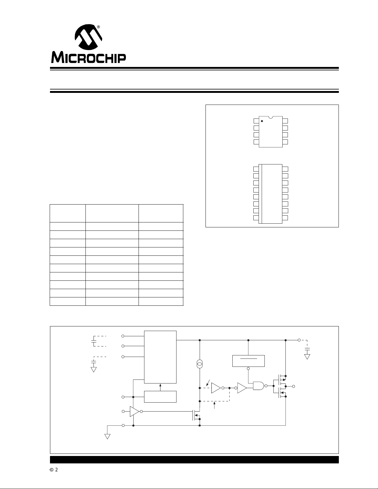
Device Selection Table
Part
Number
TC4626COE 16-Pin SOIC (Wide) -55°C to +125°C
TC4626CPA 8-PinPDIP -40°C to +85°C
TC4626EOE 16-Pin SOIC (Wide) -40°C to +85°C
TC4626EPA 8-Pin PDIP 0°C to +70°C
TC4626MJA 8-Pin CERDIP 0°C to +70°C
TC4627COE 16-Pin SOIC (Wide) -55°C to +125°C
TC4627CPA 8-PinPDIP -40°C to +85°C
TC4627EOE 16-Pin SOIC (Wide) -40°C to +85°C
TC4627EPA 8-Pin PDIP 0°C to +70°C
TC4627MJA 8-Pin CERDIP 0°C to +70°C
Package Temp. Range
Package Type
8-Pin PDIP/CERDIP
–
C1
C1
GND
1
+
2
TC4626
C2
3
TC4627
4
V
8
DD
7
IN
6
V
BOOST
5
OUT
16-Pin SOIC (Wide)
C1
NC
C1
NC
C2
NC
NC
GND
–
1
2
+
3
4
TC4626
5
TC4627
6
7
8
V
16
DD
NC
15
14
NC
IN
13
12
NC
V
11
BOOST
NC
10
OUT
9
General Description
The TC4626/TC4627 are single CMOS high speed
drivers with an on-board voltage boost circuit. These
partswork with an input supply voltagefrom4to6volts.
The internal voltage booster will produce a V
potential up to 12 volts above VIN.ThisV
regulated, so i ts voltage is dependent on the input V
voltage and output drive loading requirements. An
internalundervoltage lockoutcircuitkeepsthe outputin
a low state whenV
is enabled when V
dropsbelow 7.8 volts. Output
BOOST
is above 11.3 volts.
BOOST
BOOST
BOOST
is not
DD
Functional Block Diagram
EXT
C
1
+
EXT
C
2
NOTE: Pin numbers correspond to 8-pin package.
2002 Microchip TechnologyInc. DS21426B-page 1
C1-
C2
V
GND
DD
In
1
3
V = 2 x V
8
7
4
Voltage
Booster
DD
Clock
2
C1+
+
V
BOOST
Noninverting
TC4627
Inverting
TC4626
(Unregulated 3 x VDD)
UV LOCK
6
EXT
+
C
3
5
Output
Page 2
TC4626/TC4627
1.0 ELECTRICAL
CHARACTERISTICS
*Stresses above those listed under "Absolute Maximum
Ratings" may cause permanent damage to the device. These
are stress ratings only and functional operation of the device
at these or any other conditions above those indicated in the
Absolute Maximum Ratings*
Supply Voltage......................................................6.2V
operation sections of the specifications is not implied.
Exposure to Absolute Maximum Rating conditions for
extended periods may affectdevice reliability.
Input Voltage, Any Terminal
.....................................V
Package Power Dissipation (T
+0.3VtoGND–0.3V
S
≤ 70°C)
A
PDIP.........................................................730mW
CERDIP....................................................800mW
SOIC . .......................................................760mW
Derating Factor PDIP.......5.6 mW/°C Above 36°C
CERDIP................................................6.0mW/°C
Operating Temperature Range (Ambient)
C Version.........................................0°C to +70°C
E Version......................................-40°C to +85°C
M Version ...................................-55°C to +125°C
StorageTemperature Range..............-65°C to +150°C
TC4626/TC4627 ELECTRICAL SPECIFICATIONS
Electrical Characteristics: TA=+25°C,VDD =5V,C1=C2=C310µF unless otherwise noted.
Symbol Parameter Min Typ Max Units Test Conditions
Input
V
IH
V
IL
I
IN
Output
V
OH
V
OL
R
O
R
O
I
PK
Switching Time
t
R
t
F
t
D1
t
D2
F
MAX
Voltage Booster
R
3
R
2
F
OSC
V
OSC
UV @V
BOOST
V
START@VBOOST
V
BOOST
Logic1, High Input Voltage 2.4 — — V
Logic0, Low Input Voltage — — 0.8 V
Input Current -1 — 1 µA0V ≤ VIN ≤ V
High OutputVoltage V
–0.025 — — V
BOOST
Low Output Voltage — — 0.025 V
Output Resistance, High — 10 15 Ω I
Output Resistance, Low — 8 10 Ω I
=10mA,VDD=5V
OUT
=10mA,VDD=5V
OUT
Peak Output Current — 1.5 — A
RiseTime — 33 40 nsec Figure3-1,Figure3-2
FallTime — 27 35 nsec Figure 3-1, Figure3-2
Delay Time — 35 45 nsec Figure 3-1, Figure 3-2
Delay Time — 45 55 nsec Figure 3-1, Figure 3-2
MaximumSwitching Frequency 1.0 — — MHz VDD=5V,V
Figure 3-1
Voltage Tripler Output
—300400Ω IL=10mA,VDD=5V
Source Resistance
Voltage DoublerOutput
—120200Ω
Source Resistance
Oscillator Frequency 12 — 28 kHz
Oscillator Amplitude Measured
at C1-
4.5 — 10 V R
LOAD
=10kΩ
Undervoltage Threshold 7.0 7.8 8.5 V
Start Up Voltage 10.5 11.3 12 V
@VDD= 5V 14.6 — — V No Load
DRIVE
BOOST
>8.5V,
DS21426B-page 2
2002 Microchip TechnologyInc.
Page 3
TC4626/TC4627
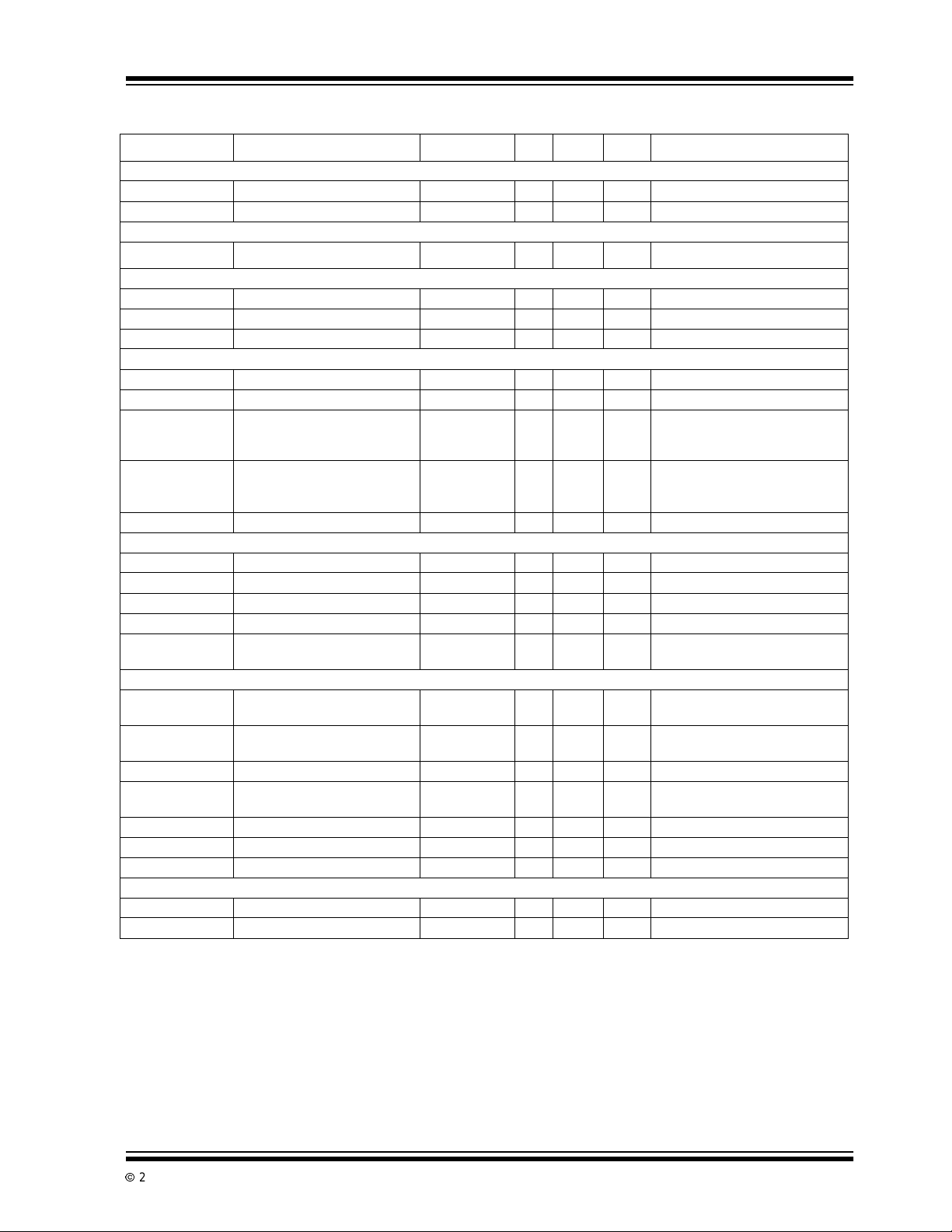
TC4626/TC4627 ELECTRICAL SPECIFICATIONS (CONTINUED)
Symbol Parameter Min Typ Max Units Test Conditions
PowerSupply
I
DD
V
DD
Electrical Characteristics: Over operating temperature range, V
Symbol Parameter Min Typ Max Units Test Conditions
Input
V
IH
V
IL
I
IN
Output
V
OH
V
OL
R
O
R
O
I
PK
Switching Time
t
R
t
F
t
D1
t
D2
F
MAX
Voltage Booster
R
3
R
2
F
OSC
V
OSC
UV @V
BOOST
V
START@VBOOST
V
BOOST
PowerSupply
I
DD
V
DD
Power Supply Current — — 2.5 mA VIN= LOW or HIGH
Supply Voltage 4.0 — 6.0 V
=5V,C1=C2=C310µF unless otherwise noted.
DD
Logic 1, High Input Voltage 2.4 — — V
Logic 0, Low Input Voltage — — 0.8 V
InputCurrent -10 — 1 µA0V ≤ VIN ≤ V
High Output Voltage V
–0.025 — — V
DRIVE
BOOST
Low Output Voltage — — 0.025 V
Output Resistance, High —
151520
25
Output Resistance, Low —
101013
15
Ω I
OUT
C&EVersion(T
M Version (T
Ω I
OUT
C&EVersion(T
M Version (T
=10mA,VDD=5V
=10mA,VDD=5V
Peak OutputCurrent — 1.5 — A
Rise Time — — 55 nsec Figure 3-1, Figure 3-2
Fall Time — — 50 nsec Figure 3-1, Figure 3-2
DelayTime — — 60 nsec Figure 3-1, Figure 3-2
DelayTime — — 70 nsec Figure 3-1, Figure 3-2
Maximum Switching Frequency 750 — — kHz VDD=5V,V
Figure3-1
Voltage Boost Output
— 400 500 Ω IL=10mA,VDD=5V
BOOST
SourceResistance
Voltage Doubler Output
— 170 300 Ω
SourceResistance
Oscillator Frequency 5 — 50 kHz
Oscillator Amplitude
Measured at C1-
4.5 — 10 V R
LOAD
=10kΩ
UndervoltageThreshold 7.0 7.8 8.5 V
Start Up Voltage 10.5 11.3 12 V
@VDD= 5V 14.6 — — V N o Load
Power Supply Current — — 4 mA VIN= LOW or HIGH
Supply Voltage 4.0 — 6.0 V
=70°Cor85°C)
A
=125°C)
A
=70°Cor85°C)
A
=125°C)
A
>8.5V,
2002 Microchip TechnologyInc. DS21426B-page 3
Page 4
TC4626/TC4627
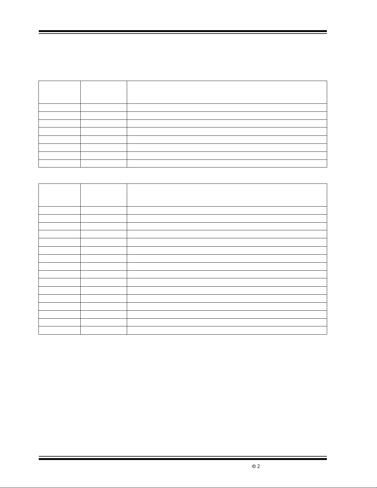
2.0 PIN DESCRIPTIONS
ThedescriptionsofthepinsarelistedinTable2-1.
TABLE 2-1: PIN FUNCTION TABLE
Pin No.
(8-Pin PDIP,
CERDIP)
1C12C1+
3C2
4 GND Ground.
5OUT
6V
7IN
8V
Pin No.
(16-Pin SOIC
Wide)
1C12 NC No connect.
3C1+
4 NC No connect.
5C2
6 NC No connect.
7 NC No connect.
8 GND Ground.
9OUT
10 NC No connect.
11 V
12 NC No connect.
13 IN
14 NC No connect.
15 NC No connect.
16 V
Symbol Description
BOOST
DD
Symbol Description
BOOST
DD
DS21426B-page 4
2002 Microchip TechnologyInc.
Page 5
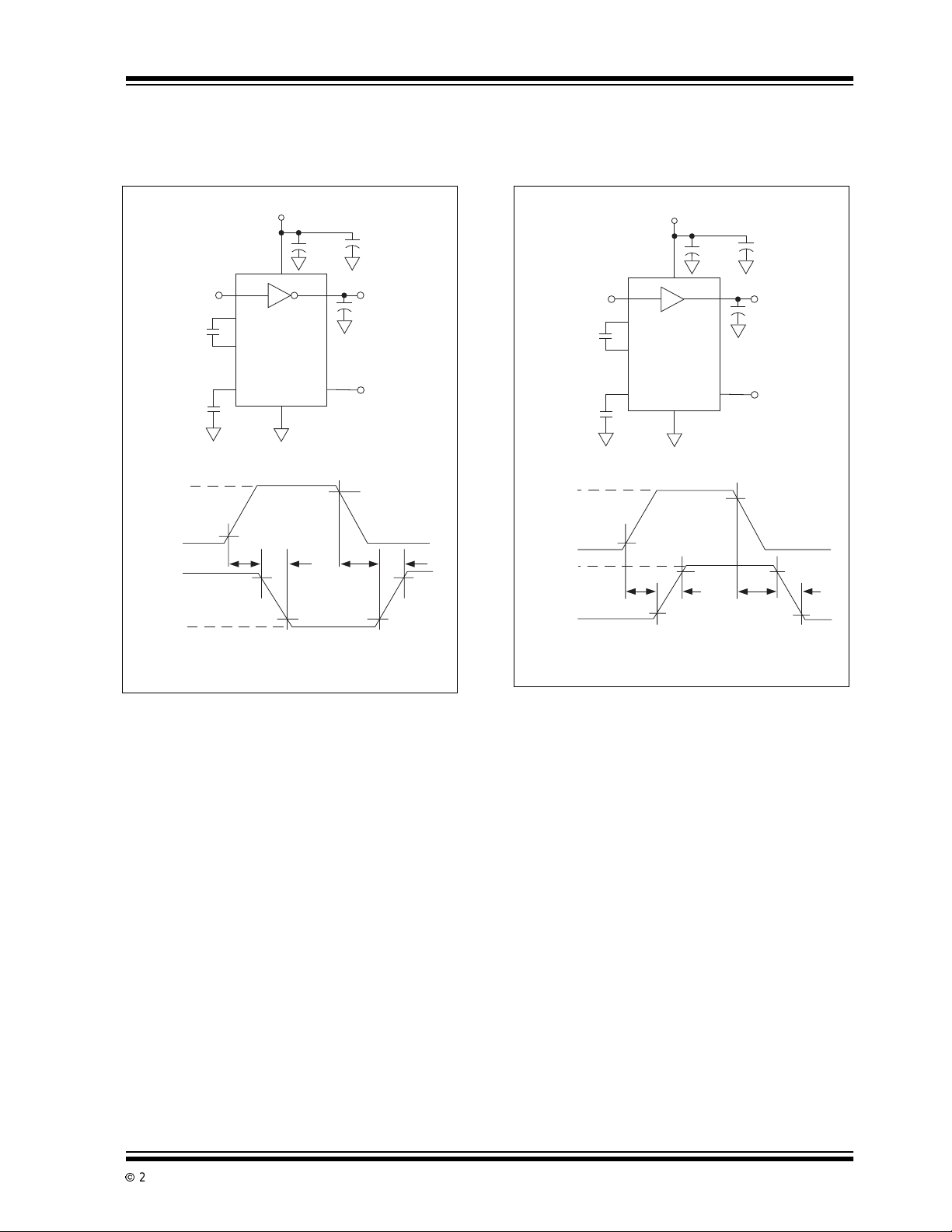
3.0 APPLICATIONS INFORMATION
t
TC4626/TC4627
FIGURE 3-1: INVERTING DRIVE R
SWITCHING TIME
V
BOOST
3
5
0.1µF Ceramic
Output
CL = 1000pF
V
DD
90%
t
D2
t
R
10%
= 5V
+5V
Input
0V
V
BOOST
Output
0V
Input: 100kHz,
square wave,
= t
RISE
C
10µF
C
10µF
FALL
Input
1
2
C
10µF
6
7
2
C1+
C1-
1
TC4626
38
C
2
4
10%
t
D1
t
F
90%
10%
≤ 10nsec
90%
FIGURE 3-2: NONINVERTING DRIVER
SWITCHING TIME
V
BOOST
5
0.1µF Ceramic
Output
CL = 1000pF
= 5V
V
DD
90%
90%
t
D2
10%
+5V
Input
0V
V
BOOST
Output
0V
Input: 100kHz,
square wave,
= t
t
RISE
C
10µF
C
10µF
FALL
1
2
C
3
10µF
6
7
Input
2
C1+
C1-
1
TC4627
38
C
2
4
10%
90%
t
D1
≤ 10nsec
10%
t
R
t
F
2002 Microchip TechnologyInc. DS21426B-page 5
Page 6

TC4626/TC4627
3.1 BOOSTER FUNCTION
The voltage booster is an unregulated voltage tripler
circuit. The tripler consists of three sets of internal
switches and three external capacitors. S1a and S1b
chargecapacitorC1 to V
FIGURE 3-3: VOLTAGE BOOSTER
potential.S2aand S2b add
DD
3 x VDD, V
S1a
S1b
C3
C2
C1
+
+
(4 to 6V)
V
DD
+
6
3
8
2
1
2 x V
BOOST
DD
C1 potential to V
input to charge C2 to 2 x VDD.S3a
DD
and S3b add C1 potential to C2 to charge C3 to 3 x
V
. The position of the switches is controlled by the
DD
internal 4 phase clock.
6
S3a
S2a
S2b
S3b
GND
4
FIGURE 3-4: POSITION OF SWITCHES
Pin 1 & 2 Waveforms
DD
DD
V
DD
DD
V
DD
0
On
Off
Pin 2
Voltage
Pin 1
Voltage
3 x V
2 x V
2 x V
S1
DS21426B-page 6
On
S2
Off
On
S3
Off
2002 Microchip TechnologyInc.
Page 7

TC4626/TC4627
4.0 TYPICAL CHARACTERISTICS
Note: The graphs and tables provided following this note are a statisticalsummary based on a limited number of
samplesandareprovidedforinformationalpurposesonly. The performancecharacteristicslistedherein are
not tested or guaranteed. In some graphs or tables, the data presented may be outside the specified
operating range ( e.g., outside specified power supply range) and therefore outside the warranted range.
16
14
12
10
8
HI (Volts)
6
OUT
V
4
2
0
5
14
12
10
8
HI (Volts)
6
OUT
V
4
2
0
5
TC4626 VOH vs. Frequency
470pF
2200pF
500 1,000 1,500 2,000 2,500 3,000 3,500
1000pF
FREQUENCY (kHz)
VS = 5V
= -55
T
A
°C
TC4626 VOH vs. Frequency
VS = 5V
= 125
T
A
470pF
2200pF
1000pF
500 1,000 1,500 2,000 2,500 3,000 3,500
FREQUENCY (kHz)
TC4626 VOH vs. Frequency
14
12
10
8
HI (Volts)
6
OUT
V
4
2
0
10
470pF
2200pF
500 1,000 1,500 2,000 2,500 3,000 3,500
1000pF
FREQUENCY (kHz)
VS = 5V
= 25
T
A
°C
Delay Time vs. Temperature
100
Input = 0-5V;
& TF <10nsec;
T
°C
Time (nsec)
R
@ <20kHz
80
t
D2
60
t
D1
40
t
RISE
20
0
-40 -20 0 20
t
FALL
TEMPERATURE (°C)
VS = 4V
C
LOAD
40 60 80
= 1000pF
100 120
Delay Time vs. Temperature
60
VS = 5V
= 1000pF
C
50
LOAD
40
t
D2
t
30
Time (nsec)
20
10
0
2002 Microchip TechnologyInc. DS21426B-page 7
D1
t
FALL
-40 -20 0 20
t
TEMPERATURE (°C)
RISE
Input = 0-5V;
T
& TF <10nsec;
R
@ <20kHz
40 60 80
100
120
50
40
30
20
Time (nsec)
10
Delay Time vs. Temperature
VS = 6V
= 1000pF
C
LOAD
t
D2
t
D1
t
t
FALL
0
-40 -20 0 20
RISE
TEMPERATURE (°C)
Input = 0-5V;
TR & TF <10nsec;
@ <20kHz
40 60 80
100
120
Page 8

TC4626/TC4627
TYPICAL CHARACTERISTICS (CONTINUED)
16
15
14
13
12
HI (Volts)
11
OUT
V
10
9
8
16
15
14
13
12
HI (Volts)
11
OUT
V
10
9
8
TC4626 VOH vs. Frequency
VS = 5V
= 25
T
°C
A
1234567
FREQUENCY x 100 kHz
TC4626 VOH vs. Frequency
VS = 5V
= 125
T
°C
A
2,200pF
1
34
2
FREQUENCY x 100 kHz
567
1,000pF
2,200pF
8
470pF
1,000pF
8
470pF
9 100
9
TC4626 VOH vs. Frequency
16
VS = 5V
15
14
13
12
HI (Volts)
11
OUT
V
10
100
= -55
T
°C
A
9
8
1234567
FREQUENCY x 100 kHz
470pF
1,000pF
2,200pF
8
100
9
DS21426B-page 8
2002 Microchip TechnologyInc.
Page 9

5.0 PACKAGING INFORMATION
3
)
)
)
)
)
)
)
)
)
)
)
)
)
)
)
)
)
)
)
)
)
)
)
.
)
)
)
)
)
)
)
.
.
)
)
)
)
)
)
)
)
)
)
)
)
)
3
)
)
)
)
)
Package marking data not available at this time.
5.1 Package Dimensions
8-Pin Plastic DIP
TC4626/TC4627
.260 (6.60
.240 (6.10
.045 (1.14
.030 (0.76
.200 (5.08
.140 (3.56
.150 (3.81
.115 (2.92
8-Pin CDIP (Narrow
.400 (10.16
.348 (8.84
.110 (2.79
.090 (2.29
.022 (0.56
.015 (0.38
.110 (2.79
.090 (2.29
.070 (1.78
.040 (1.02
.040 (1.02
.020 (0.51
.300 (7.62
.230 (5.84
.310 (7.87
.290 (7.37
.015 (0.38
.008 (0.20
.400 (10.16
310 (7.87
Dimensions: inches (mm)
.055 (1.40) MAX
.200 (5.08
.160 (4.06
.200 (5.08
.125 (3.18
.400 (10.16
.370 (9.40
.065 (1.65
.045 (1.14
.020 (0.51
.016 (0.41
.020 (0.51) MIN
.040 (1.02
.020 (0.51
.150 (3.81
.015 (0.38
.008 (0.20
.320 (8.13
.290 (7.37
.400 (10.16
.320 (8.13
Dimensions: inches (mm)
2002 Microchip TechnologyInc. DS21426B-page 9
Page 10

TC4626/TC4627
Package Dimensions (Continued)
16-Pin SOIC (Wide)
PIN 1
.413 (10.49)
.398 (10.10)
.050 (1.27) TYP.
.019 (0.48)
.014 (0.36)
.299 (7.59)
.291 (7.40)
.012 (0.30)
.004 (0.10)
.419 (10.65)
.398 (10.10)
.104 (2.64)
.097 (2.46)
8
°
MAX.
.013 (0.33)
.009 (0.23)
.050 (1.27)
.016 (0.40)
Dimensions: inches (mm)
DS21426B-page 10
2002 Microchip TechnologyInc.
Page 11

TC4626/TC4627
Sales and Support
Data Sheets
Products supportedby a preliminary DataSheetmayhave an erratasheetdescribing minor operational differences and recommendedworkarounds.To determineif an errata sheet existsfora particular device, pleasecontact one of the following:
1. Your local Microchip sales office
2. The Microchip CorporateLiteratureCenter U.S. FAX: (480)792-7277
3. The Microchip Worldwide Site (www.microchip.com)
Pleasespecify which device, revision of silicon and Data Sheet (includeLiterature #) you are using.
New Customer Notification System
Register on our web site (www.microchip.com/cn)to receive the most currentinformationon our products.
2002 Microchip Technology Inc. DS21426B-page11
Page 12

TC4626/TC4627
NOTES:
DS21426B-page12 2002 Microchip Technology Inc.
Page 13

TC4626/TC4627
Information contained in this publication regarding device
applications and the like is intended through suggestion only
and may be superseded by updates. It is your responsibility to
ensure that your application meets with your specifications.
No representation or warranty is given and no liability is
assumed by Microchip Technology Incorporated with respect
to the accuracy or use of such information, or infringement of
patents or other intellectual property rights arising from such
use or otherwise. Use of Microchip’s products as critical components in life support systems is not authorized except with
express written approval by Microchip. No licenses are conveyed, implicitly or otherwise, under any intellectual property
rights.
Trademarks
The Microchip name and logo, the Microchip logo, FilterLab,
K
EELOQ,microID,MPLAB,PIC,PICmicro,PICMASTER,
PICSTART, PRO MA TE, SEEVAL and The Embedded Control
SolutionsCompany areregiste red trademarksof MicrochipTechnologyIncorp or ated in the U.S.A. and other countries .
dsPIC, ECONOMONI TOR, FanSense, FlexROM, fuzzyLAB,
In-Circuit Serial Programming, ICSP, ICEPIC, microPort,
Migratable Memory, MPA SM, MPLIB, MPLINK, MPSIM,
MXDEV,MXLAB, PICC, PICDEM, PICDEM.net, rfPIC, Select
Mode and Total Endurance are trademarks of Microchip
TechnologyIncorporated in the U.S.A.
Serialized Quick Turn Programming (SQTP) is a service mark
of Microchip TechnologyIncorporated in t he U.S.A.
All other trademarks mentioned herein are property of their
respective companies.
© 2002, Microchip Technology Incorporated, Printed in the
U.S.A., All Rights Reserved.
Printed on recycled paper.
Microchip received QS-9000 quality system
certification for its worldwide headquarters,
design and wafer fabrication facilities in
Chandler and Tempe, Arizona in July 1999
and Mountain View, California in March 2002.
The Company’s quality system processes and
procedures are QS-9000 compliant for its
®
PICmicro
devices, Serial EEPROMs, microperipherals,
non-volatile memory and analog products. In
addition, Microchip’s quality system for the
design and manufacture of development
systemsisISO 9001certified.
2002 Microchip TechnologyInc. DS21426B-page 13
8-bit MCUs, KEELOQ®code hopping
Page 14

WORLDWIDE SALES AND SERVICE
AMERICAS
Corporate Office
2355 West Chandler Blvd.
Chandler, AZ 85224-6199
Tel: 480-792-7200 Fax: 480-792-7277
Technical Support: 480-792-7627
Web Address: http://www.microchip.com
Rocky Mountain
2355 West Chandler Blvd.
Chandler, AZ 85224-6199
Tel: 480-792-7966 Fax: 480-792-7456
Atlanta
500 Sugar Mill Road, Suite 200B
Atlanta, GA 30350
Tel: 770-640-0034 Fax: 770-640-0307
Boston
2 Lan Drive, Suite 120
Westford, MA 01886
Tel: 978-692-3848 Fax: 978-692-3821
Chicago
333 Pierce Road, Suite 180
Itasca, IL 60143
Tel: 630-285-0071 Fax: 630-285-0075
Dallas
4570 Westgrove Drive, Suite 160
Addison, TX 75001
Tel: 972-818-7423 Fax: 972-818-2924
Detroit
Tri-Atria Office Building
32255 Northwestern Highway, Suite 190
Farmington Hills, MI 48334
Tel: 248-538-2250 Fax: 248-538-2260
Kokomo
2767 S. Albright Road
Kokomo, Indiana 46902
Tel: 765-864-8360 Fax: 765-864-8387
Los Angeles
18201 Von Karman, Suite 1090
Irvine, CA 92612
Tel: 949-263-1888 Fax: 949-263-1338
New York
150 Motor Parkway, Suite 202
Hauppauge, NY 11788
Tel: 631-273-5305 Fax: 631-273-5335
San Jose
Microchip Technology Inc.
2107 North First Street, Suite 590
San Jose, CA 95131
Tel: 408-436-7950 Fax: 408-436-7955
Toronto
6285 Northam Drive, Suite 108
Mississauga, Ontario L4V 1X5, Canada
Tel: 905-673-0699 Fax: 905-673-6509
ASIA/PACIFIC
Australia
Microchip Technology Australia Pty Ltd
Suite 22, 41 Rawson Street
Epping 2121, NSW
Australia
Tel: 61-2-9868-6733 Fax: 61-2-9868-6755
China - Beijing
Microchip Technology Consulting (Shanghai)
Co., Ltd., Beijing Liaison Office
Unit 915
Bei Hai Wan Tai Bldg.
No. 6 Chaoyangmen Beidajie
Beijing, 100027, No. China
Tel: 86-10-85282100 Fax: 86-10-85282104
China - Chengdu
Microchip Technology Consulting (Shanghai)
Co., Ltd., Chengdu Liaison Office
Rm. 2401, 24th Floor,
Ming Xing Financial Tower
No. 88 TIDU Street
Chengdu 610016, China
Tel: 86-28-86766200 Fax: 86-28-86766599
China - Fuzhou
Microchip Technology Consulting (Shanghai)
Co., Ltd., Fuzhou Liaison Office
Unit 28F, World Trade Plaza
No. 71 Wusi Road
Fuzhou 350001, China
Tel: 86-591-7503506 Fax: 86-591-7503521
China - Shanghai
Microchip Technology Consulting (Shanghai)
Co., Ltd.
Room 701, Bldg. B
Far East International Plaza
No. 317 Xian Xia Road
Shanghai, 200051
Tel: 86-21-6275-5700 Fax: 86-21-6275-5060
China - Shenzhen
Microchip Technology Consulting (Shanghai)
Co., Ltd., Shenzhen Liaison Office
Rm. 1315, 13/F , Shenzhen Kerry Centre,
Renminnan Lu
Shenzhen 518001, China
Tel: 86-755-2350361 Fax: 86-755-2366086
China - Hong Kong SAR
Microchip Technology Hongkong Ltd.
Unit 901-6, Tower2, Metroplaza
223 Hing Fong Road
Kwai Fong, N.T., Hong Kong
Tel: 852-2401-1200 Fax: 852-2401-3431
India
Microchip Technology Inc.
India Liaison Office
Divyasree Chambers
1 Floor, Wing A (A3/A4)
No. 11, O’Shaugnessey Road
Bangalore, 560 025, India
Tel: 91-80-2290061 Fax: 91-80-2290062
Japan
Microchip Technology Japan K.K.
Benex S-1 6F
3-18-20, Shinyokohama
Kohoku-Ku, Yokohama-shi
Kanagawa, 222-0033, Japan
Tel: 81-45-471- 6166 Fax: 81-45-471-6122
Korea
Microchip Technology Korea
168-1, Youngbo Bldg. 3 Floor
Samsung-Dong, Kangnam-Ku
Seoul, Korea 135-882
Tel: 82-2-554-7200 Fax: 82-2-558-5934
Singapore
Microchip Technology Singapore Pte Ltd.
200 Middle Road
#07-02 Prime Centre
Singapore, 188980
Tel: 65-6334-8870 Fax: 65-6334-8850
Taiwan
Microchip Technology Taiwan
11F-3, No. 207
Tung HuaNorth Road
Taipei, 105, Taiwan
Tel: 886-2-2717-7175 Fax: 886-2-2545-0139
EUROPE
Denmark
Microchip Technology Nordic ApS
Regus Business Centre
Lautrup hoj 1-3
Ballerup DK-2750 Denmark
Tel: 45 4420 9895 Fax: 45 4420 9910
France
Microchip Technology SARL
Parc d’Activite du Moulin de Massy
43 Rue du Saule Trapu
Batiment A - ler Etage
91300 Massy, France
Tel: 33-1-69-53-63-20 Fax: 33-1-69-30-90-79
Germany
Microchip Technology GmbH
Gustav-Heinemann Ring 125
D-81739 Munich, Germany
Tel: 49-89-627-144 0 Fax: 49-89-627-144-44
Italy
Microchip Technology SRL
Centro Direzionale Colleoni
Palazzo Taurus 1 V. Le Colleoni 1
20041 Agrate Brianza
Milan, Italy
Tel: 39-039-65791-1 Fax: 39-039-6899883
United Kingdom
Microchip Ltd.
505 Eskdale Road
Winnersh Triangle
Wokingham
Berkshire, EnglandRG41 5TU
Tel: 44 118 921 5869 Fax: 44-118 921-5820
05/01/02
DS21426B-page 14
2002 Microchip Technology Inc.
 Loading...