

Page 1
N-CHANNEL 55V - 0.005 Ω -120A D²PAK/TO-220/TO-247
TYPE
STB150NF55
STP150NF55
STP150NF55
■ TYPICAL R
■ SURFACE-MOUNTING D
V
DSS
55 V
55 V
55 V
(on) = 0.005 Ω
DS
POWER PACKAGE
DESCRIPTION
This Power MOSFET is the latest dev elo pment of
STMicroelectronis unique "Single Feature Size™"
strip-based process. The resulting transistor
shows extremely high packing density for low onresistance, rugged avalanche characteristics and
less critical alignment steps therefore a
remarkable manufacturing reproducibility.
APPLICATIONS
■ HIGH CURRENT, HIGH SWITCHING SPEED
■ SOLENOID AND RELAY DRIVERS
■ MOTOR CONTROL, AUDIO AMPLIFIERS
■ DC-DC & DC-AC CONVERTERS
■ AUTOMOTIVE
R
DS(on)
<0.006
Ω
<0.006
Ω
<0.006
Ω
2
PAK (TO-263)
I
D
120 A(**)
120 A(**)
120 A(**)
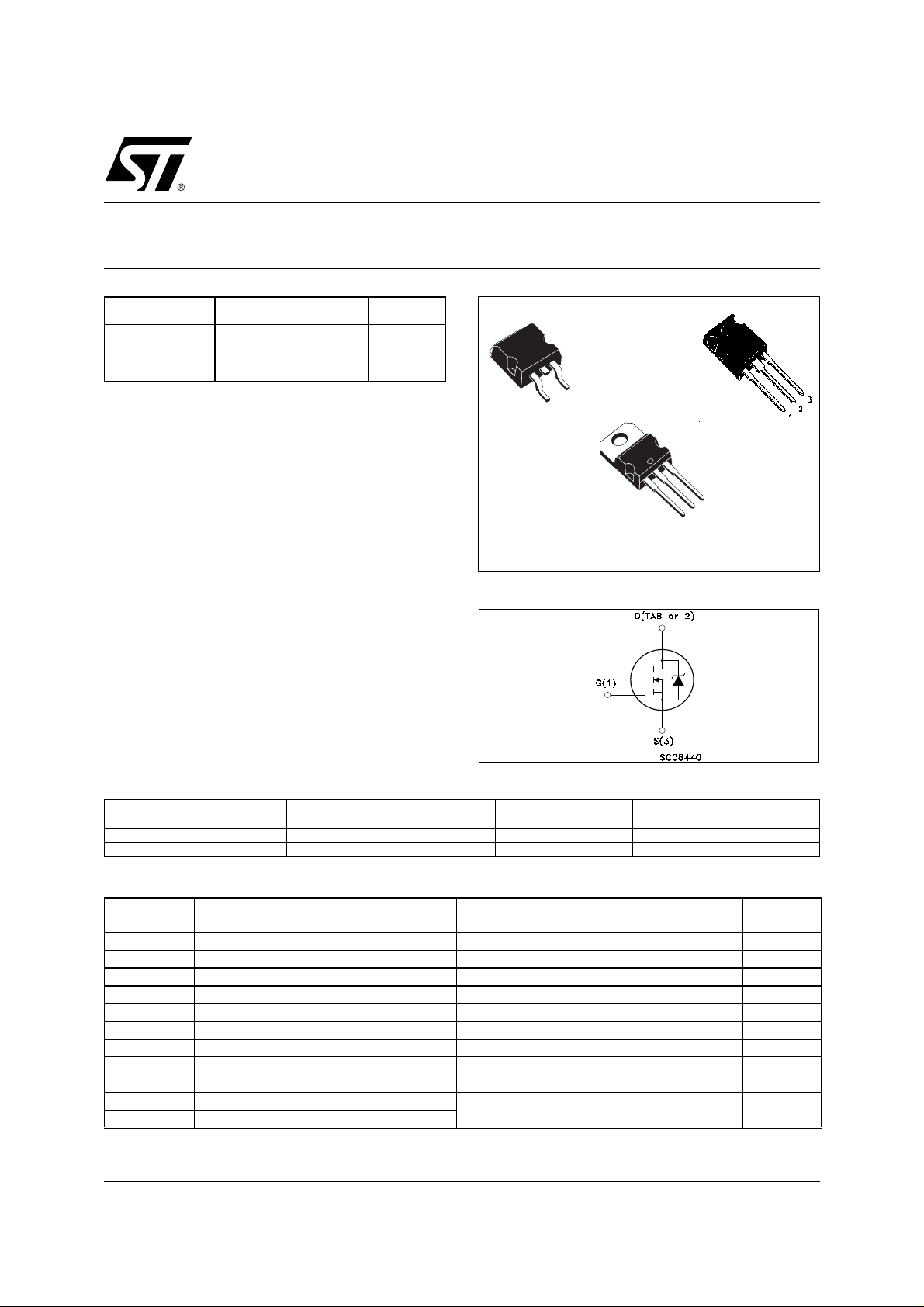
STB150NF55 STP150NF55
STW150NF55
STripFET™ II POWER MOSFET
AUTOMOTIVE SPECIFIC
3
1
D2PAK
TO-263
(Suffix “T4”)
2
1
TO-220
INTERNAL SCHEMATIC DIAGRAM
TO-247
3
Ordering Information
STB150NF55T4 B150NF55
SALES TYPE MARKING PACKAGE PACKAGING
STP150NF55 P150NF55 TO-220 TUBE
STW150NF55 W150NF55 TO-247 TUBE
2
D
PAK
T APE & REEL
ABSOLUTE MAXIMUM RATINGS
Symbol Parameter Value Unit
V
DS
V
DGR
V
GS
(**) Drain Current (continuous) at T
I
D
I
D
(
I
DM
P
tot
Drain-source Voltage (VGS = 0)
Drain-gate Voltage (RGS = 20 kΩ)
55 V
55 V
Gate- source Voltage ± 20 V
= 25°C
C
Drain Current (continuous) at TC = 100°C
•)
Drain Current (pulsed) 480 A
Total Dissipation at TC = 25°C
120 A
106 A
300 W
Derating Factor 2.0 W/°C
(1)
dv/dt
E
AS
T
stg
T
j
Pulse widt h l i m i ted by safe op erating area.
(
•)
(**) Curre nt Limited by Pac kage
Peak Diode Recovery voltage slope 8 V/ns
(2)
Single Pulse Avalanche Energy 850 mJ
Storage Temperature
Operating Junction Temperature
(1) ISD ≤120A, di/dt ≤200A/µs, VDD ≤ V
(2) Starting Tj = 25 oC, ID = 60 A, VDD = 30V
-55 to 175 °C
(BR)DSS
, Tj ≤ T
October 2002
JMAX
1/14
Page 2
STB150NF55 STP150NF55 STW150NF55
THERMA L D ATA
Rthj-case
Rthj-amb
T
Thermal Resistance Junction-case
Thermal Resistance Junction-ambient
Maximum Lead Temperature For Soldering Purpose
l
Max
Max
Typ
0.5
62.5
300
°C/W
°C/W
°C
ELECTRICAL CHARACTERISTICS (T
= 25 °C unless otherwise specified)
case
OFF
Symbol Parameter Test Conditions Min. Typ. Max. Unit
I
V
(BR)DSS
Drain-source
= 250 µA VGS = 0
D
55 V
Breakdown Voltage
V
= Max Rating
DS
V
= Max Rating TC = 125°C
DS
V
= ± 20 V
GS
1
10
±100 nA
ON
(*)
I
DSS
I
GSS
Zero Gate Voltage
Drain Current (V
GS
Gate-body Leakage
Current (V
DS
= 0)
= 0)
Symbol Parameter Test Conditions Min. Typ. Max. Unit
V
GS(th)
R
DS(on)
Gate Threshold Voltage
Static Drain-source On
= VGS I
DS
V
= 10 V ID = 60 A
GS
= 250 µA
D
24V
0.005 0.006
V
Resistance
DYNAMIC
Symbol Parameter Test Conditions Min. Typ. Max. Unit
(*)
g
fs
C
iss
C
oss
C
rss
Forward Transconductance
Input Capacitance
Output Capacitance
Reverse Transfer
Capacitance
V
15 V ID= 60 A
DS =
= 25V, f = 1 MHz, VGS = 0
V
DS
160 S
4400
1050
350
µA
µA
Ω
pF
pF
pF
2/14
Page 3
STB150NF55 STP150NF55 STW 150NF55
ELECTRICAL CHARACTERISTICS (continued)
SWITCHING ON
Symbol Parameter Test Conditions Min. Typ. Max. Unit
= 27.5 V ID = 60 A
t
d(on)
Turn-on Delay Time
t
r
Rise Time
V
DD
R
= 4.7 Ω VGS = 10 V
G
(Resistive Load, Figure 3)
Q
g
Q
gs
Q
gd
Total Gate Charge
Gate-Source Charge
Gate-Drain Charge
VDD=27.5 V ID=120A VGS= 10V
SWITCHING OFF
Symbol Parameter Test Conditions Min. Typ. Max. Unit
= 27.5 V ID = 60 A
t
d(off)
Turn-off Delay Time
t
f
Fall Time
V
DD
R
= 4.7Ω, V
G
GS
= 10 V
(Resistive Load, Figure 3)
SOURCE DRAIN DIODE
Symbol Parameter Test Conditions Min. Typ. Max. Unit
I
SD
I
SDM
V
SD
t
rr
Q
rr
I
RRM
(*)
Pulsed: P ul se duration = 300 µs, duty cycle 1.5 %.
(
•)Pulse width limited by s af e operatin g area.
Source-drain Current
(•)
Source-drain Current (pulsed)
(*)
Forward On Voltage
Reverse Recovery Time
Reverse Recovery Charge
Reverse Recovery Current
I
= 120 A VGS = 0
SD
= 120 A di/dt = 100A/µs
I
SD
V
= 25 V Tj = 150°C
DD
(see test circuit, Figure 5)
35
180
140
35
70
140
80
130
350
7.5
170 nC
120
480
1.5 V
ns
ns
nC
nC
ns
ns
A
A
ns
nC
A
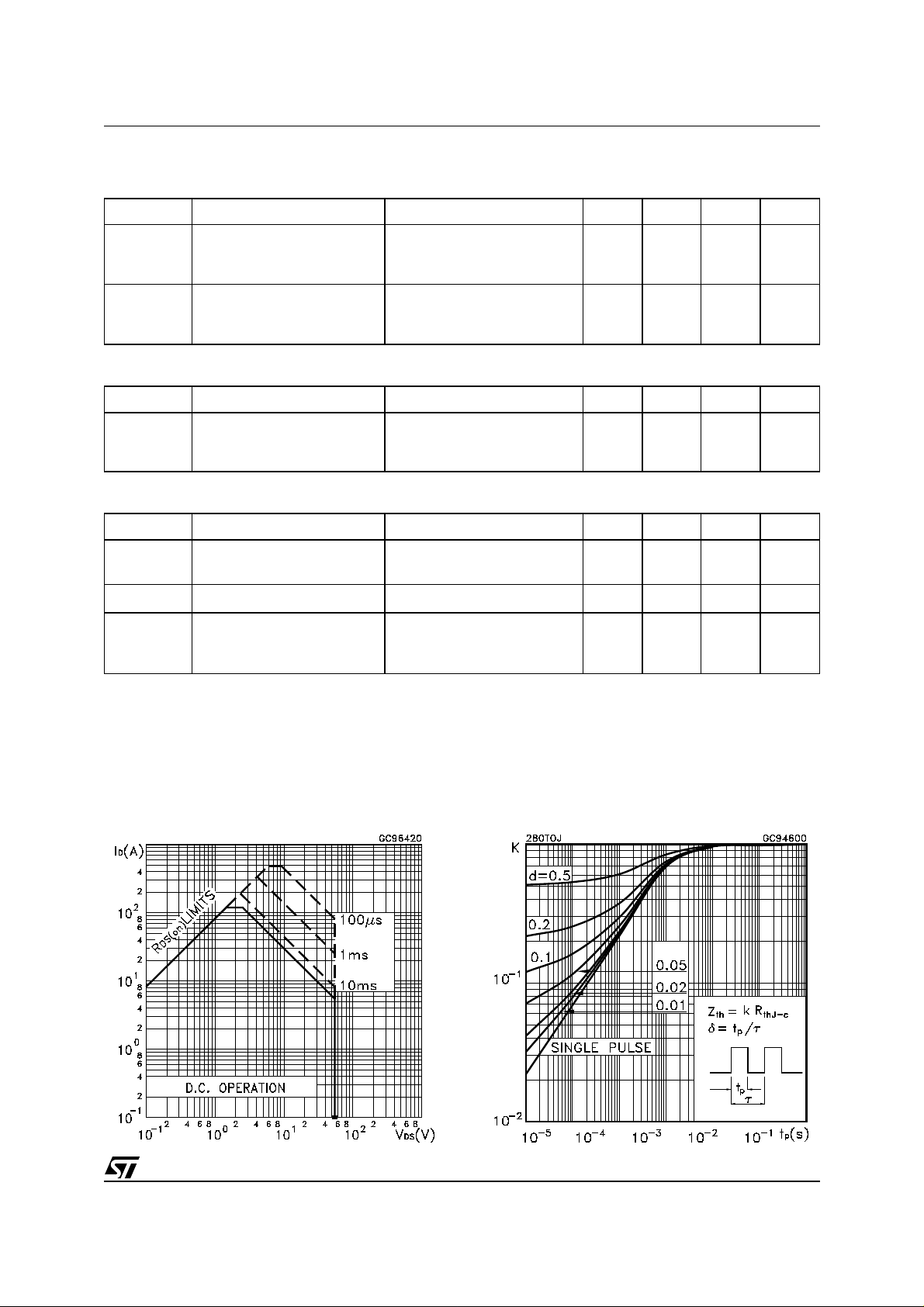
Thermal ImpedanceSafe Operating Area
3/14
Page 4
STB150NF55 STP150NF55 STW150NF55
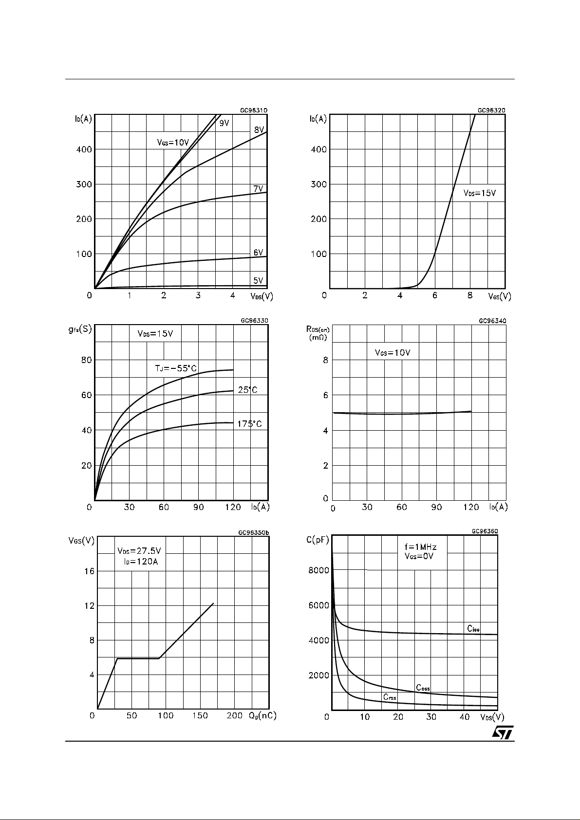
Output Characteristics Transfer Characteristics
Transconductance Static Drain-source On Resistance
Gate Charge vs Gate-source Voltage Capacitance Variations
4/14
Page 5
STB150NF55 STP150NF55 STW 150NF55
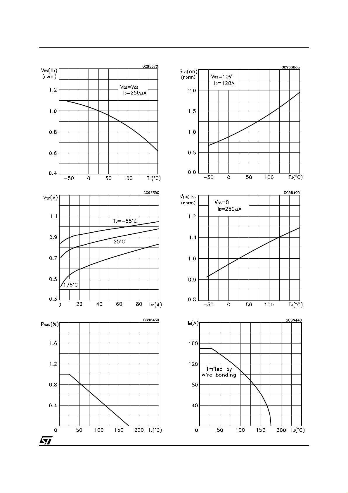
Normalized Gate Threshold Voltage vs Temperature Normalized on Resistance vs Temperature
Source-drain Diode Forward Characteristics Normalized Breakdown Voltage vs Temperature.
. .
Power Derating vs Tc Max Id Current vs Tc.
5/14
Page 6

STB150NF55 STP150NF55 STW150NF55
Thermal Resistance Rthj-a vs PCB Copper Area Max Power Dissipation vs PCB Copper Area
Allowable Iav vs. Time in Avalanche
The previous curve gives the safe operating area for unclamped inductive loads, single pulse or repetitive,
under the following conditions:
P
E
= 0.5 * (1.3 * BV
D(AVE)
= P
AS(AR)
D(AVE)
* t
AV
DSS
* IAV)
Where:
I
is the Allowable Current in Avalanche
AV
P
t
AV
To derate above 25
is the Average Power Dissipation in Avalanche (Single Pulse)
D(AVE)
is the Time in Avalanche
o
C, at fixed IAV, the following equation must be applied:
= 2 * (T
I
AV
jmax
- T
CASE
)/ (1.3 * BV
DSS
* Zth)
Where:
Z
= K * Rth is the value coming from Normalized Thermal Response at fixed pulse width equal to TAV .
th
6/14
Page 7

STB150NF55 STP150NF55 STW 150NF55
SPICE THERMAL MODEL
Parameter
CTHERM1 5 - 4 0.011
CTHERM2 4 - 3 0.0012
CTHERM3 3 - 2 0.05
CTHERM4 2 - 1 0.1
RTHERM1 5 - 4 0.09
RTHERM2 4 - 3 0.02
RTHERM3 3 - 2 0.11
RTHERM4 2 - 1 0.17
Node Value
7/14
Page 8

STB150NF55 STP150NF55 STW150NF55
Fig. 1: Unclamped Inductive Load Test CircuitFig. 1: Unclamped Inductive Load Test Circuit Fig. 2: Unclamped Inductive Waveform
Fig. 3: Switching Times Test Circuits For Resistive
Load
Fig. 4: Gate Charge Test Circuit
Fig. 3.1: Inductive Load Switching and Diode Re-
covery Ti m e s Wav e form
Fig. 4.1: Gate Charge Test Waveform
8/14
Page 9

STB150NF55 STP150NF55 STW 150NF55
Fig. 5: Unclamped Inductive Load Test Circuit Fig. 5.1: Diode Recovery Times Waveform
9/14
Page 10
STB150NF55 STP150NF55 STW150NF55
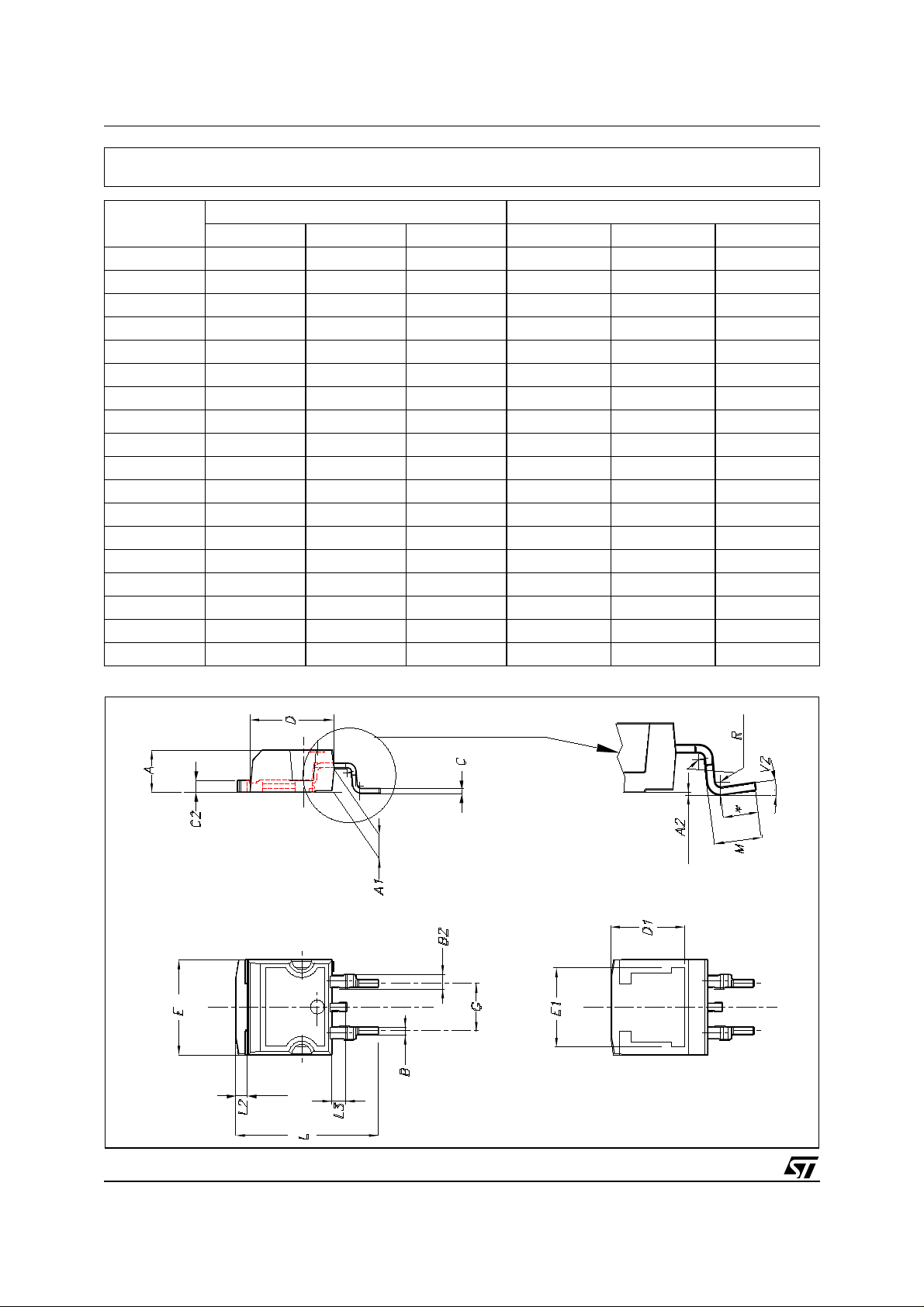
D2PAK MECHANICAL DA TA
DIM.
A 4.4 4.6 0.173 0.181
A1 2.49 2.69 0.098
A2 0.03 0.23 0.001 0.009
B 0.7 0.93 0.028 0.037
B2 1.14 1.7 0.045 0.067
C 0.45 0.6 0.018 0.024
C2 1.21 1.36 0.048 0.054
D 8.95 9.35 0.352 0.368
D1 8 0.315
E 10 10.4 0.394 0.409
E1 8.5 0.334
G 4.88 5.28 0.192 0.208
L 15 15.85 0.591 0.624
L2 1.27 1.4 0.050 0.055
L3 1.4 1.75 0.055 0.069
M 2.4 3.2 0.094 0.126
R 0.4 0.015
V2 0° 8° 0° 8°
MIN. TYP. MAX. MIN. TYP. TYP.
mm. inch.
0.106
10/14
Page 11
STB150NF55 STP150NF55 STW 150NF55
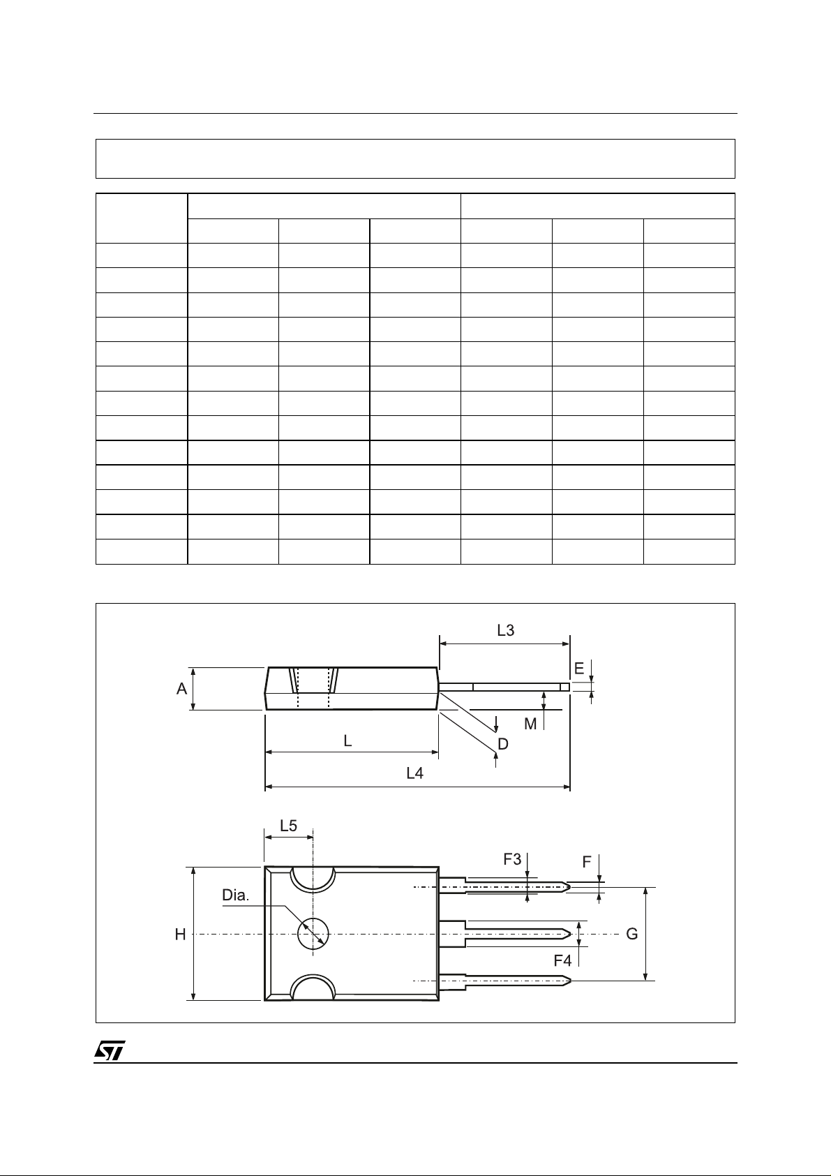
TO-247 MECHANICAL DATA
DIM.
MIN. TYP. MAX. MIN. TYP. MAX.
A 4.7 5.3 0.185 0.209
D 2.2 2.6 0.087 0.102
E 0.4 0.8 0.016 0.031
F 1 1.4 0.039 0.055
F3 2 2.4 0.079 0.094
F4 3 3.4 0.118 0.134
G 10.9 0.429
H 15.3 15.9 0.602 0.626
L 19.7 20.3 0.776 0.779
L3 14.2 14.8 0.559 0.582
L4 34.6 1.362
L5 5.5 0.217
M 2 3 0.079 0.118
mm inch
P025P
11/14
Page 12

STB150NF55 STP150NF55 STW150NF55
TO-220 MECHANICAL DATA
DIM.
A 4.4 4.6 0.173 0.181
C 1.23 1.32 0.048 0.051
D 2.40 2.72 0.094 0.107
E 0.49 0.70 0.019 0.027
F 0.61 0.88 0.024 0.034
F1 1.14 1.70 0.044 0.067
F2 1.14 1.70 0.044 0.067
G 4.95 5.15 0.194 0.203
G1 2.40 2.70 0.094 0.106
H2 10 10.40 0.393 0.409
L2 16.40 0.645
L3 28.90 1.137
L4 13 14 0.511 0.551
L5 2.65 2.95 0.104 0.116
L6 15.25 15.75 0.600 0.620
L7 6.20 6.60 0.244 0.260
L9 3.50 3.93 0.137 0.154
DIA 3.75 3.85 0.147 0.151
MIN. TYP. MAX. MIN. TYP. TYP.
mm. inch.
12/14
Page 13

STB150NF55 STP150NF55 STW 150NF55
D2PAK FOOTPRINT
TAPE AND REEL SHIPMENT (suffix ”T4”)*
TUBE SHIPMENT (no suffix)*
REEL MECHANICAL DATA
DIM.
A 330 12.992
B 1.5 0.059
C 12.8 13.2 0.504 0. 520
D 20.2 0.795
G 24.4 26.4 0.960 1.039
N 100 3.937
T 30.4 1.197
mm inch
MIN. MAX. MIN. MAX.
TAPE MECHANICAL DATA
DIM.
A0 10.5 10.7 0.413 0.421
B0 15.7 15.9 0.618 0.626
D 1.5 1.6 0.059 0.063
D1 1.59 1.61 0.062 0.063
E 1.65 1.85 0.065 0.073
F 11.4 11.6 0.449 0.456
K0 4.8 5.0 0.189 0.197
P0 3.9 4.1 0.153 0.161
P1 11.9 12.1 0.468 0.476
P2 1.9 2.1 0075 0.082
R50 1.574
T0.25 0.35 .0.0098 0.0137
W 23.7 24.3 0.933 0.956
mm inch
MIN. MAX. MIN. MAX.
* on sales type
BASE QTY BULK QTY
1000 1000
13/14
Page 14

STB150NF55 STP150NF55 STW150NF55
Information furnished is believed to be accurate and reliable. However, STMicroelectronics assumes no responsibility for the consequences
of use of such information nor for any infringement of patents or other rights of third parties which may result from its use. No license is granted
by implic ation or otherwise under any patent or p atent rights of STMi croelectr oni cs. Spec i fications mentioned i n this publicatio n are subject
to change without notice. This publication supersedes and replaces all information previously supplied. STMicroelectronics products are not
authorized for use as cri tical comp onents in life support dev i ces or systems wi t hout expres s written approval of STMi croelectr o nics.
The ST logo is registered trademark of STMicroelectronics
2002 STMi croelectr onics - All Rights Rese rved
All other na m es are the prop erty of their respectiv e owners.
Australi a - Brazil - Canada - Chin a - F i nl and - Franc e - Germany - Hong Kong - India - Israel - It al y - Japan - Mal aysia - Malta - Morocco -
Singap ore - Spain - Sw eden - Switze rl and - United Kingdom - U n i t ed States.
STMicroelectronics GROUP OF COMPANIES
http:// www.st.com
14/14
 Loading...