

Page 1
AND RECORD AMPLIFIER FOR VCR
PLAY-BACK MODE
.
LOW NOISE 68dB AMPLIFIERS FOR
2 HEADS
.
AUTOMATIC OFFSET CANCELLATION
BETWEENTHE 2 SELECTEDHEADS
.
ONE PLAY-BACKOUTPUT
.
MODESELECTIONBY LOGIC INPUT
RECORDMODE
.
ONE INTEGRATED I/I CONVERTER WITH
ACCURATE CONTROL OF TRANSCONDUCTANCE
.
RECORD AMPLIFIER WITH AUTOMATIC
PROTECTION AGAINST SHORTCIRCUIT
.
5V SUPPLYVOLTAGE
STV5712
ADVANCEDFM AUDIO PLAY-BACK
SO16 NARROW
(Plastic Micropackage)
ORDER CODE :STV5712
DESCRIPTION
The STV5712 is an advancedtwo head FM audio
recordand play-backamplifier for VCR.
PIN CONNECTIONS
1
2
3
4
5
6
7
8
April 1996
V
CC
V2
C2
H2
GND1
H1
C1
FM OUT
16
15
14
13
12
11
10
V1
I
OUT
GND2
PROT
V
MES
V
IN
SW REC
9
SW H
5712-01.EPS
1/8
Page 2
STV5712
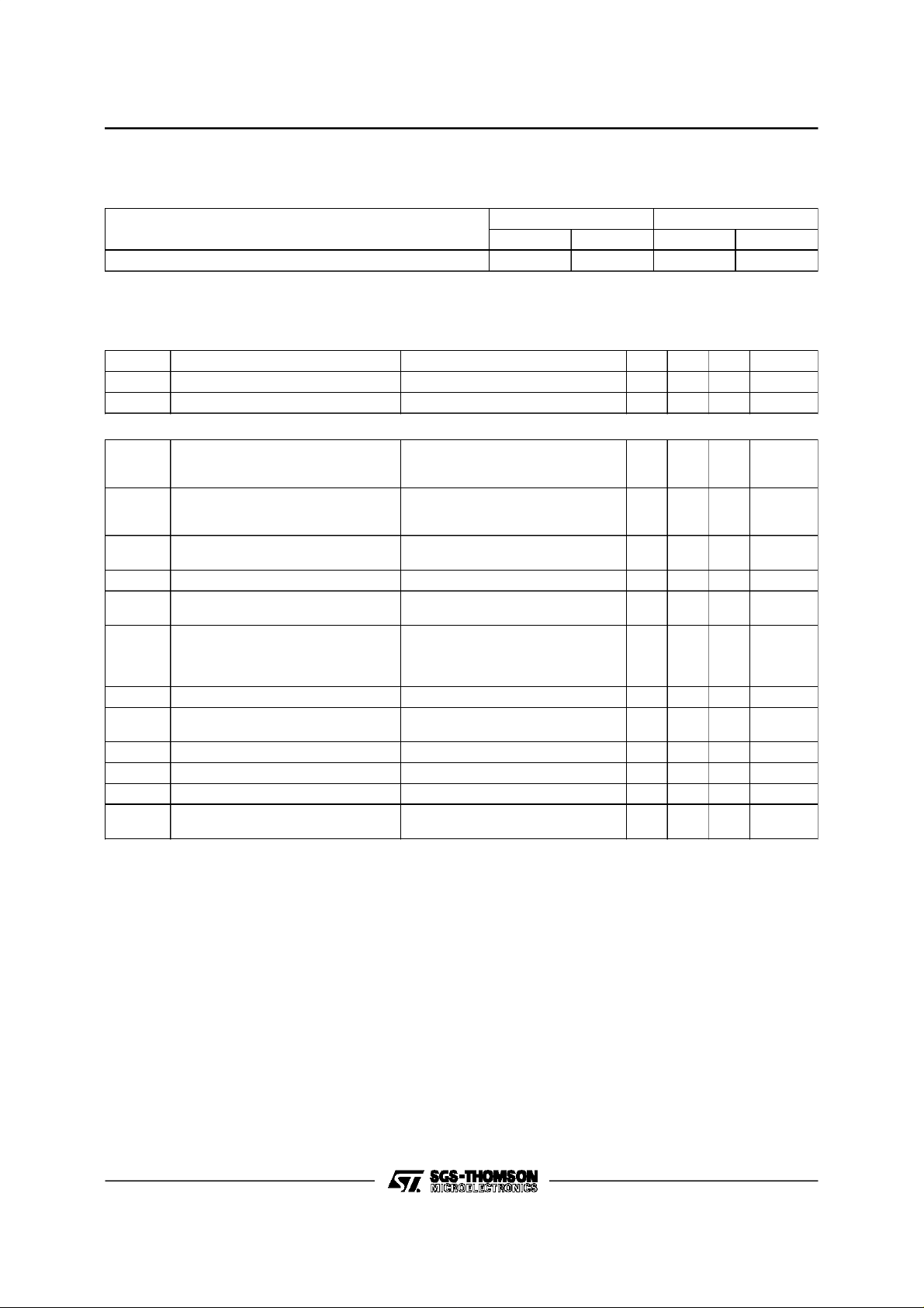
BLOCK DIAGRAM
OUT
V1
I
GND2
16
1
CC
V
14
15
234
V2
13
C2
FUNCTIONAL DESCRIPTION
STV5712 is intended for 2 heads FM audio VCR
applications.
Highperformancetechnologyallowsverylownoise
levels (current and voltage). In play-backmode a
special feature suppresses the DC offset when
switching two channels.Optimized play-backoutput stagegives to the STV5712largecapability to
directly drive a coaxial cable in order to reduce
number of externalcomponents.
Only onepower supplyis necessaryfor play-back
and record modes. The mode can be chosen
throughalogic input.Aspecialcarehasbeentaken
to avoid current peaks through the rotary transformers.
MESVIN
PROT
12
V
11
SW REC
SW H
910
S
T
V
5
7
1
2
5
6
78
H2
GND1
H1
C1
FM OUT
Duringplay-back mode,recordoutput is grounded
via an internaltransistor and during record mode
preamplifiersare turnedoff.
There is one output currentfor the two heads,the
DC current and the AC characteristicscanbe very
precisely controled with accurate external resistors.If recommendedresistancesare used,a±5%
transconductanceaccuracy is guaranted.
The recording amplifier includes a protectionsystemwhichprotectstheICand theapplicationboard
against overheatingin case of short circuit on the
recording transconductancecomponents.
STV5712is fullyprotected against ESD.
5712-02.EPS
ABSOLUTEMAXIMUMRATINGS
Symbol Parameter Value Unit
V
CC
T
J
Power Supply Voltage 6 V
Junction Temperature + 150
THERMALDATA
Symbol Parameter Value Unit
Junction-ambient ThermalResistance Typ. 100
2/8
R
th (j-a)
o
C/W
o
C
5712-01.TBL
5712-02.TBL
Page 3
STV5712
ELECTRICAL OPERATINGCHARACTERISTICS (TA=25oC unlessotherwisespecified)
Power Consumption
Parameter
= 5V 25mA 35mA 60mA 80mA
V
CC
Note : 1. R1 = 5.6Ω
Play-back Mode
=5V, no load on Pin V
V
CC
Symbol Parameter Test Conditions Min. Typ. Max. Unit
I
V
CC1
Supply Current 25 35 mA
Supply Voltage 4.75 5 5.25 V
CC
FM OUT
G
∆G
Pre-amplification Gain Sinus wave 1.6MHz
PB
Gain Difference of Output Signalon
PB
Pin FM OUT between Channel 1
and Channel 2
e
Equivalent Input VoltageNoise
N
Level
i
Equivalent Input Current Noise Pins H1, H2 3.6 5.0 pA ⁄√Hz
N
CRT Crosstalk Sinus wave 1.6MHz
Bandwidth Cut-off Frequency -3dB attenuation 50Ω in parallel on
F
LCPB
F
HCPB
Input Capacitance Pins H1, H2 45 pF
IN
Pre-amplifier Input Resistance Pins
IN
H1, H2
Output Impedance DC 30 50 Ω
PB
DC Level at Pin FMOUT 1.8 2.4 3 V
Head SwitchOffset 150 mV
DC
Second Harmonic Sinus wave 1.6MHz
PB1
V
∆V
SH
C
R
Z
DCPB
OUT
400mV
Input on Pin H1 or H2
on output,
PP
Sinus wave 1.6MHz
0.1mV
on inputs H1 or H2
PP
Input grounded via switching
transistor on Pins H1, H2
100µV
, All switches combinated
PP
the input
At 1.6MHz 600 Ω
100µV
on input 500Ω//100pF
PP
Play-Back Record (1)
Typ. Max. Typ. Max.
63 68 73 dB
1.2 dB
0.34 0.5 nV⁄√Hz
-45 -40 dB
Low
0.1 MHz
High 8
-45 -40 dB
5712-03.TBL
MHz
5712-04.TBL
3/8
Page 4

STV5712
ELECTRICAL OPERATINGCHARACTERISTICS (TA=25oC unlessotherwisespecified)(continued)
Record Mode
=5V, Load resistor 50Ω on PinI
V
CC
Transconductancenetwork definedby : R1 =5.6Ω 1% Pins PROT/V
Symbol Parameter Test Conditions Min. Typ. Max. Unit
I
CC2
I
OUT
I
max
I
BIAS
TR Transconductance V
Z
OUT
SH
F
LCREC
F
HCREC
Current Supply VCC=5V 60 80 mA
Max. Record Current 70 mA
Biasing Current of the record
amplifier
Output Resistance 7 100 kΩ
Second Harmonic Output Current 40mAPPat1.6MHz -43 -38 dB
REC
Bandwidth Cut-off Frequency -3dB attenuation
Maximum Input Current
on Pin PROT
Maximum SaturationVoltage
on Pin PROT
Input Resistance Equivalent value of R3 resistor 500 700 900 Ω
OUT
MES
R2 =1kΩ 1% PinsV
R3 =750Ω 1% Pins V
MES/VIN
IN
33 40 47 mA
= 200mV
IN
PP
Output current 60mA
PP
Low
220 mA/V
High 5
5V on Pin PROT 150 250 400 mA
Input current 50mA 100 150 mV
0.1 MHz
MHz
PP
5712-05.TBL
SwitchingLevels
Symbol Parameter Test Conditions Min. Typ. Max. Unit
V
SWH1
V
SWL1
I
SWH1
I
SWL1
V
SWH2
V
SWL2
I
SWH2
I
SWL2
t
ON1
t
OFF1
t
ON2
t
OFF2
Head SelectionPin SW
Mode SelectionPin SW REC
Selection Pin SW Transient
Response
Selection Pin SW REC
Transient Response
Head number 1 (high level) 2.4 V
CC
Head number 2 (low level) 0 1.5 V
Input current (high level) 20 50 µA
Output current (low level) 20 50 µA
Record mode (high level) 2.4 V
CC
Play-back mode(low level) 0 1.5 V
Input current (high level) 20 50 µA
Output current (low level) 20 50 µA
Delay time selection ON (output
250 500 ns
signalappears on Pin FM OUT)
Delay time selection OFF (output
250 500 ns
signaldisappears on Pin FM OUT)
Delay time selection ON (output
signalappears on Pin I
OUT
)
Delay time selection OFF (output
440 µs
1.3 10 ms
signalappears on Pin FM OUT)
V
V
5712-06.TBL
4/8
Page 5

STV5712
ELECTRICAL OPERATINGCHARACTERISTICS (TA=25oC unlessotherwisespecified)(continued)
Power Supply
Symbol Parameter Test Conditions Min. Typ. Max. Unit
V
SVR Supply Voltage Rejection 0.5mV
Positive Supply VoltagePin V
CC
CC
75µVPPon Pin H1, H2
on Pin V
PP
Measurement on Pin FM OUT
INPUT/OUTPUTS EQUIVALENT INTERNAL DIAGRAM
CC
4.75 5 5.25 V
15 20 dB
5712-07.TBL
Pins : C1, C2
Pin : FM OUT
4k
Ω
1.5pF
7.5k
400
Pin : SW
V
CC
15k
V
CC
10k
Ω
47k
Ω
Ω
1k
Ω
5712-03.EPS
Pin : V
MES
V
CC
5pF
500
Ω
800
Ω
0.5pF
Ω
Ω
10k
Ω
5712-04.EPS
V
REC
6pF
75
Ω
18
Ω
5712-05.EPS
5712-06.EPS
5/8
Page 6

STV5712
INPUT/OUTPUTS EQUIVALENT INTERNAL DIAGRAM (continued)
Pin : V
IN
750
Ω
Pin : PROT
750
Pin s : V1,V
V
CC
Ω
6pF
2
V
CC
V1
5712-07.EPS
Pin : V
CC
5712-08.EPS
0V/5V
800
Ω
Pin : I
VCC5V
6/8
OUT
800
5712-09.EPS
5712-10.EPS
Pins : H1, H2
V
CC
120k
Ω
ES D
protection
2.8mA
in play-back
V
MES
5712-11.EPS
Ω
2.1V
H1
H2
5712-12.EPS
Page 7

APPLICATIONDIAGRAM
R3
750
STV5712
V
IN
C7 22nF
Ω
R1
5.6
Ω
I
11
R2
1k
Ω
111213141516
910
R4 10k
C8
1nF
S
SW-REC
Ω
SW-H
T
V
5
7
I
12
1
234
C2
22nF
578
6
C3
C4
22nF
22nF
C1
22nF
C6
22nF
1
2
GND
FM
OUT
C5
22
µ
L1 22µH
F
V
CC
5712-13.EPS
7/8
Page 8

STV5712
PACKAGE MECHANICAL DATA
16 PINS- PLASTICMICROPACKAGE (SO NARROW)
Dimensions
Min. Typ. Max. Min. Typ. Max.
A 1.75 0.069
a1 0.1 0.25 0.004 0.009
a2 1.6 0.063
b 0.35 0.46 0.014 0.018
b1 0.19 0.25 0.007 0.010
C 0.5 0.020
c1 45
D 9.8 10 0.386 0.394
E 5.8 6.2 0.228 0.244
e 1.27 0.050
e3 8.89 0.350
F 3.8 4.0 0.150 0.157
L 0.4 1.27 0.016 0.050
M 0.62 0.024
S8
Millimeters Inches
o
(typ.)
o
(Max.)
PM-SO16N.EPS
SO16N.TBL
Informationfurnished is believed to be accurate and reliable. However,SGS-THOMSON Microelectronicsassumes no responsibility
for the consequences of use of such information nor for anyinfringement of patents or other rights of third partieswhich mayresult
from its use. No licenceis granted by implication orotherwise under any patent orpatent rights of SGS-THOMSON Microelectronics.
Specifications mentioned in this publication are subject to change without notice. This publication supersedes and replaces all
informationpreviously supplied. SGS-THOMSON Microelectronics products arenot authorizedfor use as critical components in life
support devicesor systems withoutexpress written approvalof SGS-THOMSON Microelectronics.
1996 SGS-THOMSON Microelectronics -All Rights Reserved
Purchase of I
2
I
C Patent. Rights to usethese components in a I2C system,is granted provided that thesystem conforms to
Australia - Brazil - Canada- China- France - Germany -Hong Kong- Italy- Japan - Korea - Malaysia - Malta - Morocco
The Netherlands - Singapore - Spain -Sweden -Switzerland -Taiwan - Thailand - United Kingdom - U.S.A.
2
C Componentsof SGS-THOMSON Microelectronics,conveys a license under the Philips
2
the I
C Standard Specificationsas defined by Philips.
SGS-THOMSON Microelectronics GROUP OF COMPANIES
8/8
 Loading...