

Page 1

MONOCHIP TELETEXT AND VPS DECODER
.
COMPLETE TELETEXT AND VPS DECODER
INCLUDING AN 8 PAGE MEMORY ON A SINGLE CHIP
.
UPWARD SOFTWARE COMPATIBLE WITH
PREVIOUS SGS-THOMSON’s MULTICHIP
SOLUTIONS (SAA5231, SDA5243, STV5345)
.
PERFORM PDC SYSTEM A (VPS) AND PDC
SYSTEM B (8/30/2) DATA STORAGE SEPARATLY
.
DEDICATED "ERROR FREE" OUTPUT FOR
VALID PDC DATA
.
INDICATION OF LINE 23 FOR EXTERNAL
USE
.
SINGL E +5V SUPPLY VOLTAGE
.
SINGLE 13.875MHz CRYSTAL
.
REDUCED SET OF EXTERNAL COMPONENTS, NO EXTERNA L ADJUSTMEN T
.
OPTIMIZED NU MBER OF DIGITAL SIGNALS
REDUCING EMC RADIATION
.
HIGH DENSITY CMOS TEC HNOLO GY
.
DIGITAL DATA SLICER AND DISPLAY
CLOCK PHASE LOCK LOOP
.
28 PIN D I P & SO PACKAGE
STV5348
STV5348/H - STV5348/T
WITH 8 INTEGRATED PAGES
DIP28
(Plastic Package)
ORDER CODE :
STV5348 West European
STV5348/H East European
STV5348/T Turkish & European
SO28
(Plastic Package)
ORDER CODE :
STV5348D West European
STV5348D/H East European
STV5348D/T Turkish & European
PIN CONNECTIONS
DESCRIPTION
The STV5348 decoder is a computer-controlled
teletext device including an 8 page internal memory . Data slicing and capturing extracts the teletext
information embedded in the composite video signal. Control is accomplished via a two wire serial
2
I
C bus . Chip address is 22h. Internal ROM provides a character set suitable to display text using
up to seven national languages. Hardware and
software features allow selectable master/slave
synchronization configurations. The STV5348 also
supports facilities for reception and display of current level protocol data.
September 1998
CVBS
MA/SL
V
DDA
POL
STTV/LFB
FFB
V
SSD
RGB REF
BLAN
COR
1
2
3
4
5
6
7
R
8
G
9
B
10 19
11 18
12 17
13 16
14 15ODD/EVEN
28
27
26
25
24
23
22
21
20
CBLK
TEST
V
SSA
V
SSO
XTI
XTO
V
DDD
VCR/TV
RESERVED
DV
L23
SDA
SCL
Y
5348-01.EPS
1/22
Page 2

STV5348 - STV5348/H - STV5348/T
PIN DESCRIPTION
o
Pin N
1 CVBS Input Composite Video Signal Input through Coupling Capacitor 9
2
3V
4 POL Input STTV / LFB / FFB Polarity Selection 12
5 STTV/LFB Output / Input Composite Sync Output, Line Flyback Input 15
6 FFB Input Field Flyback Input 12
7V
8 R Output Video Red Signal 13
9 G Output Video Green Signal 13
10 B Output Video Blue Signal 13
11 RGBREF Supply DC Voltage to define RGB High Level 13
12 BLAN Output Fast Blanking Output TTL Level 15
13
14
15 Y Output Open Drain Foreground Information Output 15
16 SCL Input Serial Clock Input 16
17 SDA Input/ Output Serial Data Input/Output 17
18 L23 Output Line 23 Identification 15
19
20 RESERVED Test To be connected to V
21
22 V
23 XTO Crystal Output Oscillator Output 13.875MHz 14
24 XTI Crystal Input Oscillator Input 13.875MHz 14
25 V
26 V
27 TEST Test Grounded to V
28 CBLK Input / Output To connect Black Level Storage Capacitor 28
Symbol Function Description Figure
MA/SL Input Master/Slave Selection Mode 11
DDA
SSD
Analog Supply +5V -
Ground Digital Ground -
COR Output Open Drain Contrast Reduction Output 15
ODD/EVEN Output 25Hz Output Field synchronized for non-interlaced display 15
DV Output VPS Data Valid 15
through a resistor 15
SSD
VCR/TV Input PLL Time Constant Selection 15
DDD
SSO
SSA
Digital Supply +5V -
Ground Oscillator Ground Ground Analog Ground -
SSA
11
5348-01.TBL
BLOCK DIAGRAM
2/22
CVBS
CBLK
VCR/TV
XTI
XTO
V
SSO
SCL
SDA
STTV/LFB
1
28
21
24
23
25
16
17
STV5348
POLFFB
MA/SL
CLAMPING
SYNCHRONIZING
DATA EXTRACTION
OSCILLATOR
FREQUENCY
SYNTHETIZER
TIME BASE
2
I C BUS
INTERFACE
7 26 1411
V
V
SSD
SSA
L23
18
Data
Clock
27
TEST
V
DATA DECODING
DATA
PROCESSING
Data
8 PAGES
MEMORY
Data
Address
DISPLAY
INTERFACE
RGB REF
ODD/EVEN
DDD
CTRL
Address
V
CTRL
DDA
3225 6 2 4
19
20
12
13
8
9
10
15
DV
TEST
BLAN
COR
RED
GREEN
BLUE
Y
5348-02.EPS
Page 3

STV5348 - STV5348/H - STV5348/T
ABSOL UT E MAXIMUM R ATING S
Symbol Parameter Value Unit
V
DD
V
V
O
∆
V
DD
T
oper
T
stg
Positive Supply Voltage on V
Input Voltage (any input) - 0.3, VDD + 0.5 V
I
DDD
and V
DDA
- 0.3, 6.0 V
Output Voltage (any output) - 0.3, VDD + 0.5 V
Difference between V
DDD
, V
DDA
0.25 V
Operating Ambient Temperature 0, + 70
Storage Temperature - 40, + 150
o
C
o
C
5348-02.TBL
ELECTRICAL CHARACTERISTICS
= 5V, VSS = 0V, TA = 25oC)
(V
DD
Symbol Parameter Min. Typ. Max. Unit
SUPPLIES
V
I
I
DD
DDD
DDA
Supply Voltage 4.75 5 5.25 V
V
Pin Supply Current 30 mA
DDD
V
Pin Supply Current 5 mA
DDA
INPUTS
CBLK
I
BLKO
I
BLKI
Source Current (V
Sink Current (V
CBLK
= 2V, V
CBLK
= 2V, V
= 0V) 80
CVBS
= 1V)) - 10
CVBS
CVBS
CVBSI Video Input Amplitude (peak to peak) 1 V
CVBSC Input Capacitance 10 pF
t
SYNC
V
CLAMP
I
CLPH
I
CLPL
Delay from CVBS to TCS Output from STTV Pin 200 ns
Clamping Level at Synchro Pulse 0 mV
High Level Clamp Current (CVBS = V
Low Level Clamp Current (CVBS = V
+ 1V) 5
CLAMP
- 0.3V) - 400
CLAMP
MA/SL, POL, LFB, FFB, VCR/TV
V
V
IH
I
IL
C
Input Voltage Low Level - 0.3 + 0.8 V
IL
Input Voltage High Level 2 V
Input Leakage Current (VI = 0 to V
Input Capacitance 10 pF
I
) - 10 + 10
DDD
DD
SCL, SDA
V
V
I
f
SCL
tR, t
C
IL
IH
IL
Input Voltage Low Level - 0.3 + 1.5 V
Input Voltage High Level 3 V
Input Leakage Current (VI = 0 to VDD) - 10 + 10
Clock Frequency (SCL) 100 kHz
Input Rise and Fall Time (10 to 90%) 2
F
Input Capacitance 10 pF
I
DD
RGB REF
V
I
I
Input Voltage VDD - 0.5V V
I
DDVDD
Input Current 50 mA
+ 0.3V V
µ
A
µ
A
µ
A
µ
A
V
µ
A
V
µ
A
µ
s
5348-03.TBL
3/22
Page 4

STV5348 - STV5348/H - STV5348/T
ELECTRICAL CHARACTERISTICS -
= 5V, VSS = 0V, TA = 25oC (continued)
V
DD
Symbol Parameter Min. Typ. Max. Unit
OUTPUTS
RGB
V
V
C
t
R
Output Low Voltage (IOL = 2mA) 0.4 V
OL
Output High Voltage (IOH = -2mA, RGB REF = VDD/2) RGB REF - 0.5 RGB REF V
OH
Load Capacitance 50 pF
L
, t
Rise and Fall Time (10 to 90%) 20 ns
F
BLAN
V
V
C
t
R
Output Low Voltage (IOL = 2mA) 0 0.4 V
OL
Output High Voltage (IOH = -0.2mA) VDD - 0.5 V
OH
Load Capacitance 50 pF
L
, t
Rise and Fall Time (10 to 90%) 20 ns
F
ODD/EVEN, STTV, L23, DV
V
V
C
t
R
Output Low Voltage(I
OL
Output High Voltage (IOH = -0.2mA) VDD - 0.8 V
OH
Load Capacitance 50 pF
L
, t
Rise and Fall Time (10 to 90%) 20 ns
F
COR AND Y (with Pull up to V
V
I
C
OLL
Output Low Voltage (IOL = 2mA) 0 0.5 V
OL
Load Capacitance 25 pF
L
t
Fall Time (RL = 1.2kΩ, V
F
Output Leakage Current -10 +10
= 2mA) 0 0.5 V
OL
)
DDD
- 0.5V to 1.5V) 50 ns
DDD
DD
SDA
V
C
Output Low Voltage (IOL = 3mA) 0 0.5 V
OL
t
Fall Time (3.0 to 1.0V) 200 ns
F
Load Capacitance 400 pF
L
CRYSTAL OSCILLATOR
XTI, XTO
f
XTAL
R
BIAS
C
Crystal Frequency 13.875 MHz
Internal Bias Resistance 0.4 1 3 M
Input Capacitance 7pF
I
TIMING
SERIAL BUS (referred to VIH = 3V, VIL = 1.5V)
Clock :
t
LOW
t
HIGH
t
SU, DAT
t
HD, DAT
t
SU, STO
t
BUF
t
HD, STA
t
SU, STA
●
Low Period
●
High Period
4
4
Data Set-up Time 250 ns
Data Hold Time 170 ns
Stop Set-up Time from Clock High 4
Start Set-up Time following a Stop 4
Start Hold Time 4
Start Set-up Time following Clock Low to High Transition 4
V
µ
A
Ω
µ
s
µ
s
µ
s
µ
s
µ
s
5348-04.TBL
4/22
Page 5

STV5348 - STV5348/H - STV5348/T
Figure 1 :
Figure 2 :
SDA
Display Output Timing
LSP
(TCS)
R.G.B.Y
(1)
R.G.B.Y
(1)
Serial Bus Timing
t
BUF
04.66 64
0
0
16.67 56.67
lines 42 to 291 inclusive
(and 355 to 604 inclusive interlaced)
(b) FIELD RATE
t
LOW
40ms
(a) LINE RATE
all timings in ms
31229141
line numbers
5348-03.EPS
t
F
SCL
SDA
VIH = 3V , VIL = 1.5V
Figure 3 :
Master Synchronization Mode - Hardware Configuration
+5V
MA/SL
POL
t
HD,STA
t
R
t
HD,DAT
t
SU,STA
t
HIGH
t
SU,STO
t
SU,DAT
5348-04.EPS
Output signal on STTV Pin :
Synchro
1
Extractor
Line PLL Line PLL
POL grounded
VCS when R1D2 = 0
TCS when R
2
= "0"
R
1D2
4
VCS
TCS
R
1D2
= "1"
Bit R1D
2
I2C
Control
POL to V
DD
VCS when R
TCS when R
1D2
1D2
1D2
= 1
= 0
= 1
STTV
5348-05.EPS
5/22
Page 6
STV5348 - STV5348/H - STV5348/T
Figure 4 :
Figure 5 :
Master Synchronization Mode - Delivered Composite Synchronization Signal
VCS, TCS
(interlaced)
621
622
623
624
(308)
(309)
(310)
VCS, TCS
(interlaced)
309 310 311 312 313 314
TCS
(non-interlaced)
308 309 310 311 312 1 2 3 4 5 6
The number positions indicate the end of lines.
Internal signals :
- VCS composite synchro from CVBS signal,
- TCS Teletext composite synchro.
(311)
625
(312)
12 3456
315
316
317
(1)
(2)
(3)
(4)
318
(5)
Slave Synchronization Mode
LFB
SCS
6
FFB
+5V
MA/SL
+5V
2 5
POL
4
319
(6)
5348-06.EPS
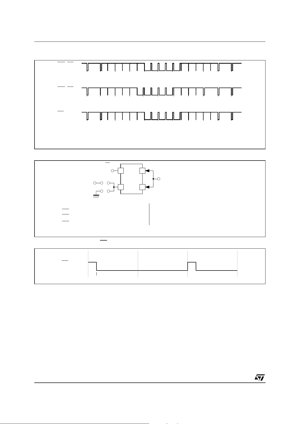
Figure 6 :
POL grounded, Inputs Signals :
LFB line flyback synchro on Pin 5
are
FFB field flyback synchro on Pin 6
or SCS synchro composite signal on Pins 5 and 6
Note : R1D0 and R1D1 must be set to 1.
Data Valid Timing (
DV)
Field 0
DV for
VPS Data
Line 16
POL to VDD, Inputs Signals :
are LFB line flyback synchro on Pin 5
FFB field flyback synchro on Pin 6
or SCS synchro composite signal on Pins 5 and 6
5348-07.EPS
Field 1 Field 0
5348-08.EPS
6/22
Page 7

FUNCTIONAL DESCRIPTION
I - Displayable Page Memory Map
The organization of a page-memory is shown in
Figure 7.
The display area consists of 25 rows of 40 characters per row.
The organization is as follows :
- Row zero contains the page header :
•
The first seven characters (0 - 6) are used for
messages regarding the operational status.
•
The eighth character is an alphanumeric control
character either "white" or "green" defining the
"search" status of the page. When it is "white"
the operational state is normal and the header
appears white ; when it is "green" the opera-
Figure 7 :
Page Memory Organization
Fixed characters
7 Status
Characters
Alphanumerics white
for normal,
green on search
24 characters from page header
rolling on page search
STV5348 - STV5348/H - STV5348/T
tional state cor responds to the "s earch mode"
and the header appears green.
•
The following twenty-four characters give the
header of the requested page when the system
is in search mode.
•
The last eight characters display the time of day .
- Row number twenty-four is used by the microprocessor for the display of information, or used
to display X/24 colored key data according to
R0D7 bit.
- Row twenty-five comprises ten bytes of control
data concerning the received page (see T able 1)
and fourteen free bytes which can be used by the
microprocessor.
8 scrolling
time characters
ROW
17248
MAIN PAG E DISPLAY AREA
row free for status (R0D7 = 0) or packet X/24 (R0D7 = 1)
10 14
0
1
2
3
4
5
6
7
8
9
10
11
12
13
14
15
16
17
18
19
20
21
22
23
24
25
10 bytes for received
page information
14 bytes free
for use by
µ
C
5348-09.EPS
7/22
Page 8

STV5348 - STV5348/H - STV5348/T
FUNCTIONAL DESCRIPTION
(continued)
II - Ghost Row Storage Organization
Row Address
of Stored Data
0 0000
1 0001
2 0010
3 0011
4 0100
5 0101
6 0110
7 0111
8 1000
9 1001
10 1010
11 1011
12 1100
13 1101
14 1110
15 0 0 1 0 X / 28 Conditional access
16 0000
17 0001
18 0100
19 0101
20 X / 24 Page extension stored here if R0D7 = 0
21 X / 25 Page extension
22 0 0 0 0 X / 28 Color definition
23 X X X X 8 / 30 * * Broadcasting service data packet
24 0 0 0 1 X/28 Character set designation
25 ** Not used
* Packet 8/30 storage :
** See table 2 for VPS data storage in chapter 5
Table 1 :
Row 25 Received Page Control Data Format
Designation
Code
Row (Packet)
Number
X / 26 Enhanced display facilities
X / 27
8/30/0,1 : chapter 4, row23
8/30/2,3 : chapter 5, row23
8/30/4 to 15 : chapter 6, row23
Function
Editorial
Linked pages
Composition
Page related data
stored in chapter
corresponding to
level 1 data,
i.e. For 0 goes in 4
" 1 " " 5
" 2 " " 6
" 3 " " 7
5348-05.TBL
D0 PU0 PT0 MU0 MT0 HU0 HT0 C7 C11 MAG0 0
D1 PU1 PT1 MU1 MT1 HU1 HT1 C8 C12 MAG1 0
D2 PU2 PT2 MU2 MT2 HU2 C5 C9 C13 MAG2 0
D3 PU3 PT3 MU3 C4 HU3 C6 C10 C14 0 0
D4 HAM HAM HAM HAM HAM HAM HAM HAM
FOUND 0
D5 000000000PBLF
D6 0000000000
D7 0000000000
COLUMN0123456789
Page number : - MAG = magazine, PU = page units, PT = page tens.
Page sub-code : - MU = minutes units, MT = minutes tens, HU = hours units, HT = hours tens.
PBLF = page being looked for,
FOUND = low for page found, HAM = hamming error in byte, C4-14 = control bits.
8/22
5348-06.TBL
Page 9

STV5348 - STV5348/H - STV5348/T
FUNCTIONAL DESCRIPTION
III - VPS DATA
(see Table 2)
VPS data are stored in r ow 25 chapter 5 as shown
in T able 2 when VPS enable bit (D4 of R8 register)
is set. VPS data bits are decoded and stored in a
received area with biphase error bit.
8/30/2 data are stored as received (without hamming decoding) in Row 23 chapter 5 according to
Table 2. .
8/30 packet and VPS data decoding is the responsibility of the control software. The decoder simply
stores transmitted data.
(continued)
a read/write and R11B is read only.
The automatic succession on a byte by byte basis
is indicated by the arrows in Table 3.
In the normal operating mode TB should be set to
logic level 0.
After power-up the contents of the registers are as
follows : all bits in registers R0 to R11A are cleared
to zero with the exception of bits D0 and D1 in
registers R5 and R6 which are set to logical one.
After power-up all the memory bytes are preset to
hexadecimal value 20H (space) with the exception
2
C Bus Register Map
IV - I
(see Table 3)
Registers R0 to R10 are write only whilst R11A is
T ab le 2 :
Column 012345678910111213141516171819
8/30/2 (Row 23) D Initial Page b13 b14 b15 b16 b17 b18 b19 b20 b21 b22 b23 b24 b25
VPS (Row 25) Received Page Information B11 B12 B13 B14 B15
Column 20 21 22 23 24 25 26 27 28 29 30 31 32 33 34 35 36 37 38 39
8/30/2 (Row 23) Status Display
VPS (Row 25) B4 B5
PDC Data Storage in Chapter 5
of the byte corresponding to row 0 of column 7 of
chapter 0 which is set to the value cor responding
to "alpha white" hexadecimal value 07H.
5348-11.TBL
T ab le 3 :
D7 D6 D5 D4 D3 D2 D1 D0
X24
POSITION
(1) 7 + P/
(1) BANK
(1) (1) (1) PRD4 PRD3 PRD2 PRD1 PRD0
(1) (1) (1) (1) (1) A2 A1 A0
BKGND
OUT
BKGND
OUT
STATUS
ROW
BTM/TOP
(1) (1) (1) VPS
(1) (1) (1) R4 R3R2R1R0
(1) (1) C5 C4 C3 C2 C1 C0
D7
(R/W)
60Hz00 000DATA
(1) Reserved register bits : must be set to 0
Register Specification
FREE
RUNNING
PLL
8 BIT
SELECT
A2
BKGNDINCOR
BKGNDINCOR
CURSOR
ON/
D6
(R/W)D5(R/W)
0 DISABLE
ACQ.
ON/OFF
ACQ.
CCT
A1
OUT
OUT
CONCEAL/
OFF
REVEAL
ROLLING
HEADER
GHOST
ROW
ENABLE
ACQ.
CCT
A0
COR
IN
COR
IN
TOP/
BOTTOM
ENABLE
D4
(R/W)D3(R/W)D2(R/W)D1(R/W)D0(R/W)
(1) EVEN
DEW/
FULL
FIELD
TB ST AR T
TEXT
OUT
TEXT
OUT
SINGLE/
DOUBLE
HEIGHT
CLEAR
MEM.
OFF
TCS
ON
COLUMN
SC2
TEXTINPON
TEXTINPON
BOX ON24BOX ON
A2 A1 A0
(1) SEL 11B
T1 T0
START
COLUMN
SC1
OUT
OUT
1-23
QUAL
START
COLUMN
SC0
PON
IN
PON
IN
BOX ON
0
V
CS
QUAL
↵
↵
↵
↵
↵
↵
↵
↵
↵
R0 Mode 0
R1 Mode 1
R2 Page request address
R3 Page request data
R4 Display chapter
R5 Display control (normal)
Display control
R6
(newsflash / subtitle)
R7 Display mode
R8 Active chapter
R9 Active row
R10 Active co l u mn
R11A Active data
R11B Status
5348-07.TBL
9/22
Page 10

STV5348 - STV5348/H - STV5348/T
FUNCTIONAL DESCRIPTION
2
C Bus Register Map
IV - I
(continued)
(continued)
IV .1 - Registers Functions
Register Function Bit(s) Description
SEL 11B (D0) Selection of register 11B (D0 = 1) or 11A (D0 = 0)
R0
Address
00H
R1
Address
01H
R2
Address
02H
R3
Address
03H
R4
Address
04H
R5
Address
05H
R6
Address
06H
R11 adressing and
pin functions control
Operating mode
controls
Addressing
information for
a page request
Data relative to the
requested page
(see Table 3)
Selection of one of
eight pages to
display
Display control for
normal operation
Display control for
news-flash subtitle
generation
EVEN OFF (D2) Control of
DISABLE ROLLING
HEADER
FREE RUNNING
PLL (D6)
X/24 POSITION (D7) D7 = 0, packet X/24 stored to chapter 4 to 7/row 20
T1 (D1) T0 (D0)
00
01
10
11
TCS ON (D2) Master Mode (
DEW / FULLFIELD
(D3)
GHOST ROW
ENABLE (D4)
ACQUISITION
ON / OFF (D5)
7 bits + parity or 8 bits
without parity (D6)
SC0, SC1, SC2
(D0, D1, D2)
TB (D3) Test bit equal to "0" in the normal working mode.
A0, A1 (D4, D5) Address a group of four consecutive pages currently used
A2 (D6) Address of one of the two groups of four pages for
PRD0 - PRD4
(D0 - D4)
A0, A1, A2
(D0, D1, D2)
PON (D0, D1) Picture on (IN: D0, OUT: D1)
TEXT (D2, D3) Text on (IN: D2, OUT: D3)
COR (D4, D5) Contrast reduction on (IN: D4, OUT: D5)
BKGND (D6, D7) Background color on (IN: D6, OUT: D7)
IN / OUT Enable inside/outside the box
See R5 See R5
(D2 = 0) or grounded (D2 = 1)
D4 = 1, Disable rolling header
D4 = 0, Normal operation
D6 = 0, PLL locks on line frequency
D6 = 1, to force free running mode
D7 = 1, packet X/24 stored to chapter 0 to 3/row 24
Character display line control :
312.5/312.5 line MIX - mode with interlace
312/313 line TEXT - mode without interlace
312/312 line Terminal mode without interlace
External synchronization. SCS mode (scan field synchro)
Slave Mode (MA/SL Pin 2 = VDD)
Selection of field flyback mode or full channel mode
(D3 = 1) for recovering of Teletext data.
Selection of ghost row mode (D4 = 1)
Control of acquisition operation (D5 = 0 enables
acquisition)
Selection of received data format either 7 bits with parity
(D6 = 0) or 8 bits without parity (D6 = 1).
Address the first column of the on chip page request RAM
to be written.
for data acquisition.
acquisition in normal mode.
Written data in the page request RAM, starting with the
columns addressed by SC0,SC1,SC2.
Chapter selection.
ODD/EVEN pin : EVEN signal output
case POL Pin 4 = 0
D2 = 0, Pin 5 =
D2 = 1, Pin 5 = TCS
No effect
MA/SL Pin 2 = 0)
VCS
5348-08.TBL
10/22
Page 11

STV5348 - STV5348/H - STV5348/T
FUNCTIONAL DESCRIPTION
2
C Bus Register Map
IV - I
IV .1 - Registers Functions
Register Function Bit(s) Description
R7
Address
07H
R8 Memory access
R9 to R11A
Address
08H to 0BH*
R11B
Address
0BH*
* Reading of R11A or R11B is determined by register 0, bit D0. However, write operation is always performed on R11A register.
Display mode
Active row address (R9), active column address (R10).
Data contained in R11A read (written) from (to) memory by microprocessor via I
Status
(continued)
(continued)
(continued)
BOX ON 0, 1-23,24
(D0, D1, D2)
TOP / BOTTOM
Single / Double Height
(D4/D3)
Conceal / Reveal (D5) Conceal Reveal Function
Cursor ON/
STATUS ROW
BTM / TOP (D7)
VPS Enable (D4) D4 = 1 Enable VPS acquisition and DV signal output.
Clear Memory (D3) D4 = 1 Clear memory.
Chapter Address
VCS QUAL (D0) Good VCS quality signal detected (D0 = 1).
DATA QUAL (D1) Good TELETEXT signal (D1 = 1).
OFF (D6) Cursor position given by row/column value of R9/R10
(D2, D1, D0)
50/60Hz (D7) If D1 = 0 frame frequency is 50Hz (only valid with good
The "boxing" function is enabled on row 0,1-23 and 24 by
D0, D1 and D2 set to one.
X0 = Normal
01 = double height Rows 0 to 11
11 = double height Rows 12 to 23
The row 24 is displayed before the "Main text Area" (lines
0-23) or after (D7 = 0).
Chapter selected with A2A1A0 (D2, D1, D0) R4.
Chapter selection
Bad VCS quality signal detected (D0 = 0).
Bad TELETEXT signal (D1 = 0).
VCS)
2
C.
5348-09.TBL
T ab le 4 :
START
COLUMN
The abbreviations have the same significance as in Table 1 with the exception of the "DO CARE" entries. It is only when this bit is "1"
that the corresponding digit is taken into consideration on page request. For example, a page defined as "normal" or one defined as
"timed" may be selected.
If "
Register R3
PRD4 PRD3 PRD2 PRD1 PRD0
0 Do care magazine
1 Do care page tens PT3 PT2 PT1 PT0
2 Do care page units PU3 PU2 PU1 PU0
3 Do care hours tens X X HT1 HT0
4 Do care hours units HU3 HU2 HU1 HU0
5 Do care minutes tens X MT2 MT1 MT0
6 Do care minutes units MU3 MU2 MU1 MU0
HOLD" is low the page is held. The addressing of successive bytes via the I2C is automatic.
HOLD MAG2 MAG1 MAG0
V - Character Sets
The complete character set with 8-bit decoding is
given in Table 5.
Characters in columns 0 and 1 are normally displayed as blanks. Black dots represent the character shape whereas white dots represent the
background.
Each character can be identified by a pair of corre-
sponding row and column integers : for example
the character "3" may be indicated by 3/3.
A rectangle may be represented as follows :
The characters 8/6, 8/7, 9/5, 9/7 are used as spe-
cial characters, always in conjunction with 8/5.
The 13 national characters are placed in columns
with bit 8 = 0.
5348-10.TBL
11/22
Page 12

STV5348 - STV5348/H - STV5348/T
FUNCTIONAL DESCRIPTION
T ab le 5 :
STV5348 Complete Character Set (with 8 bit codes) - West European Languages
1
1
15
1
1
0
1
14
1
1
1
0
13
1
1
0
0
1
1
1
0
912
0
1
0
0
8
0
1
7a
1
1
1
0
0
0
0
0
or 1
0
0
or 1
0
0
0
b8b7b6b
BIT
7
6a
0
1
1
6
1
0
5
1
0
0
4
1
1
1
3a
0
1
1
3
0
0
1
2a
0
0
1
2
0
1
0
10
0
0
0
0
5
S
black
graphics
graphics
black
alphanu m eri cs
alphanumerics
column
0
000
0
1
1
0000
row
1
b
2
b
3
b
4
b
(continued)
red
green
graphics
red
green
alphanumerics
2
010001101000101011110001001101010111100110111101111
blue
yellow
graphics
graphics
yellow
alphanumerics
3
graphics
magenta
blue
magenta
alphanumerics
alphanumerics
4
5
Case using C12 C13 C14 = 001 (German Set)
* These control characters are reserved for compatibility with other data codes.
** These control characters are presumed before each row begins
cyan
graphics
cyan
alphanumerics
6
110
0
**
white
display
conceal
flash
8
graphics
continuous
**
steady
9
graphics
**
white
alphanumerics
7
*
ESC
graphics
separated
**
end box
start box
10
11
**
**
new
black
background
background
**
height
height
double
norma l
12
13
**
hold
release
graphics
graphics
*
*
SI
SO
14
15
5348-10.EPS
12/22
Page 13

STV5348 - STV5348/H - STV5348/T
FUNCTIONAL DESCRIPTION
T ab le 6 :
STV5348/H Complete Character Set (with 8 bit codes) - East European Languages
1
1
1
1
0
1
1
1
1
0
1
1
0
0
1
1
1
0
0
11
0
0
0
1
1
1
0
0
1
1
0
(continued)
1
0
1
0
0
0
1
0
0
1
0
0
0
1
0
0
1
0
0
1
0
1
0
0
0
0
0
5
b
b
b
S
b
33a4 5 66a77a8 912131415
22a
12
colum n
row
1
2
3
4
red
black
graphics
graphics
red
black
alphanumerics
alphanumerics
0
1
1000
0000
green
yellow
graphics
graphics
green
yellow
alphanumerics
alphanumerics
2
3
0010
0011
blue
graphics
graphics
magenta
blue
magenta
alphanumerics
alphanumerics
4
5
0100
0101
cyan
graphics
cyan
alphanumerics
6011078
or 1
0
or 1 0
0
0
0
b8b7b6b
BIT
Case using C12 C13 C14 = 001 (Rumanian Set)
* These control characters are reserved for compatibility with other data codes.
** These control characters are presumed before each row begins
white
graphics
**
white
alphanumerics
0111
**
display
conceal
graphics
continuous
**
flash
steady
9
1000
1001
*
graphics
separated
**
end box
10
1010
**
ESC
black
background
**
height
normal
start box
11
12
1011
1100
**
new
background
*
height
double
13
1101
**
hold
release
graphics
*
SI
SO
14
15
1110
1111
graphics
5348-??.EPS
13/22
Page 14

STV5348 - STV5348/H - STV5348/T
FUNCTIONAL DESCRIPTION
T ab le 7 :
STV5348/T Complete Character Set (with 8 bit codes) - Turkish European Languages
1
1
1
1
0
1
1
1
1
0
1
1
0
0
1
1
1
0
0
11
0
0
0
1
1
1
0
0
1
1
0
(continued)
1
0
1
0
0
0
1
0
0
1
0
0
0
1
0
0
1
0
0
1
0
1
0
0
0
0
0
5
b
b
b
S
b
33a4 5 66a77a8 912131415
22a
12
column
row
1
2
3
4
red
black
graphics
graphics
black
alphanumerics
alphanumerics
0
0000
graphics
red
alphanumerics
1
2
1000
0010
green
green
graphics
alphanumerics
3
0011
yellow
yellow
blue
graphics
graphics
blue
alphanumerics
alphanumerics
4
0100
5
0101
cyan
graphics
mage nt a
cyan
magenta
alphanumerics
60110
or 1
0
or 1 0
0
0
0
b8b7b6b
BIT
Case using C12 C13 C14 = 001 (German Set)
* These control characters are reserved for compatibility with other data codes.
** These control characters are presumed before each row begins
**
white
display
conceal
graphics
**
white
alphanumerics
7
0111
flash
8
1000
graphics
continuous
**
steady
9
1001
*
ESC
graphics
separated
**
end box
start box
10
11
1010
1011
**
**
new
black
**
normal
12
1100
background
height
background
height
double
13
1101
**
hold
release
graphics
graphics
*
*
SI
SO
14
15
1110
1111
5348-??.EPS
14/22
Page 15

STV5348 - STV5348/H - STV5348/T
FUNCTIONAL DESCRIPTION
(continued)
The basic set of the 96 characters is shown in
Table 8.The location of the 13 national characters
T ab le 8 :
Basic charact e r set .
2/0
2/1
2/2
2/3
2/4
2/5
2/6
National
Character
National
Charact er
3/0
3/1
3/2
3/3
3/4
3/5
3/6
4/0
4/1
4/2
4/3
4/4
4/5
4/6
National
Character
are shown in Table 8 whilst full national character
sets are depicted in Tables 9, 10 and 11.
5/0
5/1
5/2
5/3
5/4
5/5
5/6
6/0
6/1
6/2
6/3
6/4
6/5
6/6
National
Charact er
7/0
7/1
7/2
7/3
7/4
7/5
7/6
2/7
2/8
2/9
2/10
2/11
2/12
2/13
2/14
2/15
3/7
3/8
3/9
3/10
3/11
3/12
3/13
3/14
3/15
4/7
4/8
4/9
4/10
4/11
4/12
4/13
4/14
4/15
5/7
5/8
5/9
5/10
5/11
5/12
5/13
5/14
5/15
National
Character
National
Charact er
National
Charact er
National
Character
National
Character
6/7
6/8
6/9
6/10
6/11
6/12
6/13
6/14
6/15
7/7
7/8
7/9
7/10
7/11
7/12
7/13
7/14
7/15
National
Character
National
Character
National
Character
National
Character
5348-11.EPS
15/22
Page 16

LANGUAGE
ENGLISH
GERMAN
SWEDISH
ITALIAN
FRENCH
SPANISH
C12 C13 C14
PHCB (1)
000
001
001
011
100
101
2/3 2/4 4/0 5/11 5/12 5/ 13 5/14 5/15 6/0 7/11 7/12 7/13 7/14
CHA RA CTER P OSITIO N ( COLUMN/ ROW)
STV5348 - STV5348/H - STV5348/T
FUNCTIONAL DESCRIPTION
Table 9 :
STV5348 Character Set - West European Languages
(continued)
Note 1 :
Where PHCB are the Page Header Control bits. Other Combinations default to English. Only the above characters change with the PHCB. All others
characters in the basic set are shown in Table 5.
16/22
5348-12.EPS
Page 17

LANGUAGE
ENGLISH
GERMAN
TURKISH
ITALIAN
FRENCH
SPANISH
C12 C13 C14
PHCB (1)
000
001
01
011
100
101
2/3 2/4 4/0 5/11 5/12 5/ 13 5/14 5/15 6/0 7/11 7/12 7/13 7/14
CHA RA CTER P OSITIO N ( COLUMN/ ROW)
1
STV5348 - STV5348/H - STV5348/T
FUNCTIONAL DESCRIPTION
Table 10 :
STV5348/H Character Set -
East European Languages
(continued)
Table 11 :
STV5348/T Character Set -
Turkish European Languages
CHA RA CTER P OSITIO N ( COLUMN/ ROW)
2/3 2/4 4/0 5/11 5/12 5/ 13 5/14 5/15 6/0 7/11 7/12 7/13 7/14
011
PHCB (1)
000
C12 C13 C14
LANGUAGE
Note 1 :
POLISH
Where PHCB are the Page Header Control bits. Other
Combinations default to German. Only the above characters
change with the PHCB. All others characters in the basic set are
shown in Table 7.
001
001
GERMAN
SWEDISH
SERBO-CROAT
1
1
10
11
RUMAN I A M
CZECHOSLOVAK
5348-??.EPS
Note 1 :
Where PHCB are the Page Header Control bits. Other
Combinations default to Turkish. Only the above characters
change with the PHCB. All others characters in the basic set are
shown in Table 7.
17/22
5348-??.EPS
Page 18

STV5348 - STV5348/H - STV5348/T
FUNCTIONAL DESCRIPTION
Figure 8 :
Character Format
Alphanumerics and
Graphics 'space'
character
2/0
Contiguous
graphics character
7/6
(continued)
Alphanumerics
character
Separated
graphics character
2/13
7/6
Alphanumerics or
blast-through
alphanumerics
character 4/8
Separated
graphics character
7/15
Alphanumerics
character
7/15
Contiguous
graphics character
7/15
Background
=
Color
Display
=
Color
5348-17.EPS
18/22
Page 19

I/O PIN ELECTRICAL SCHEMATICS
Figure 9 :
Analog 1 (CVBS)
V
DDA
STV5348 - STV5348/H - STV5348/T
Figure 10 :
Analog 2 (CBLK)
V
DDA
Figure 11 :
Pins 2, 27
MA/SL, TEST
Figure 13 :
CVBS 250
1
Input A
PRGB
V
DDD
RGB REF
11
CBLK 250
W
V
SSA
5348-18.EPS
Figure 12 :
V
DDA
450
W
Pins 4, 6
28
Input D
V
450
SSA
V
W
5348-19.EPS
DDD
W
POL, FFB
V
SSA
450
W
5348-20.EPS
Figure 14 :
XTI
P???
W
V
SSD
V
DDD
W
750k
XTO450
450
W
2324
5348-21.EPS
Figure 15 :
STTV/LFB, BLAN, COR,
DV, RESERVED, VCR/TV
INOUT
Pins 5, 12, 13, 14,
15, 18, 19, 20, 21
ODD/EVEN, Y, L23,
Pins
8, 9, 10
R, G, B
V
SSD
V
SSD
V
DDD
450
W
V
SSD
5348-22.EPS
5348-24.EPS
5348-23.EPS
19/22
Page 20

STV5348 - STV5348/H - STV5348/T
I/O PIN ELECTRICAL SCHEMATICS
Figure 16 :
PSCL
SCL
450
V
DDD
W
16
V
APPLICATION DIAGRAM
0.1mF 0.1mF
1
CVBS
1mF
SL
MA
0.1mF
+5V
+5V
2
3
4
5
6
7
8
9
10
11
MA/SL
V
POL
STTV/LFB
FFB
V
R
G
B
RGB REF
+5V
+5V
(continued)
SSD
DDA
SSD
S
T
V
5
3
4
8
Figure 17 :
5348-25.EPS
CBLK
TEST
V
V
XTO
V
VCR/TV
SSA
SSO
XTI
DDD
PSDA
28
27
26
25
24
13.875MHz
23
22
21
20
47kW**
19
18
SDA
17
TV
VCR
C1*
C2*
450
V
SSD
+5V
V
DDD
W
5348-26.EPS
+5V
1mF
10nF
BLAN
12
COR
13
ODD/EVEN
14
* Value according to used crystal, C1 = C2 = 2 * C
Example : C1 = C2 = 56pF, C
** Depending on application. Please refer to our video application lab.
Remark :
all the power supply inputs must be switched on at the same time (c onnected to the same source).
LOAD
= 30pF.
LOAD
20/22
SDA
SCL
17
16
15
Y
5348-27.EPS
Page 21

PACKAGE MECHANICAL DATA
28 PINS - PLASTIC DIP
STV5348 - STV5348/H - STV5348/T
PM-DIP28.EPS
Dimensions
Min. Typ. Max. Min. Typ. Max.
Millimeters Inches
a1 0.63 0.025
b 0.45 0.018
b1 0.23 0.31 0.009 0.012
b2 1.27 0.050
D 37.4 1.470
E 15.2 16.68 0.598 0.657
e 2.54 0.100
e3 33.02 1.300
F 14.1 0.555
I 4.445 0.175
L 3.3 0.130
DIP28.TBL
21/22
Page 22

STV5348 - STV5348/H - STV5348/T
PACKAGE MECHANICAL DATA
28 PINS - PLASTIC MICROPACKAGE (SO)
PM-SO28.EPS
Dimensions
Min. Typ. Max. Min. Typ. Max.
Millimeters Inches
A 2.65 0.104
a1 0.1 0.3 0.004 0.012
b 0.35 0.49 0.014 0.019
b1 0.23 0.32 0.009 0.013
C 0.5 0.020
c1 45
o
(typ.)
D 17.7 18.1 0.697 0.713
E 10 10.65 0.394 0.419
e 1.27 0.050
e3 16.51 0.65
F 7.4 7.6 0.291 0.299
L 0.4 1.27 0.016 0.050
S8
Information furnished is believed to be accurate and reliable. However, STMicroelectronics assumes no responsibility for the
consequences of use of such information nor for any infringement of patents or other rights of third parties which may result from
its use. No licence is granted by implication or otherwise under any patent or patent rights of STMicroelectronics. Specifications
mentioned in this publication are subject to change without notice. This publication supersedes and replaces all information
previously supplied. STMicroelectronics products are not authorized for use as critical components in life support devices or syst em s
without express written approv al of STMi cr oelec troni cs.
Purchase of I
Rights to use these components in a I
Australia - Brazil - Canada - China - France - Germany - Italy - Japan - Korea - Malaysia - Malta - Mexico - Morocco - The Netherlands
Singapore - Spain - Sweden - Switzerland - Taiwan - Thailand - United Kingdom - U.S.A.
The ST logo is a registered trademark of STMicroelectronics
1998 STMicroelectronics - All Rights Reserved
©
2
C Components of STMicroelectronics, conveys a license under the Philips I2C Pate n t .
2
C Standard Specifications as defined by Phili ps.
the I
STMicroelectronics GROUP OF COMPANIES
2
C system, is granted provided that the system conforms to
o
(max.)
SO28.TBL
22/22
 Loading...