

Page 1
MONOCHIPTELETEXTAND VPS DECODER
.
COMPLETETELETEXTAND VPS DECODER
INCLUDINGAN 4 PAGEMEMORYON A SINGLECHIP
.
UPWARD SOFTWARE COMPATIBLE WITH
PREVIOUS SGS-THOMSON’s MULTICHIP
SOLUTIONS(SAA5231,SDA5243,STV5345)
.
PERFORM PDC SYSTEM A (VPS) ANDPDC
SYSTEM B (8/30/2) DATA STORAGE SEPARATLY
.
DEDICATED “ERROR FREE” OUTPUT FOR
VALIDPDCDATA
.
INDICATION OF LINE 23 FOR EXTERNAL
USE
.
SINGLE+5V SUPPLYVOLTAGE
.
SINGLE13.875MHz CRYSTAL
.
REDUCED SET OF EXTERNAL COMPONENTS,NO EXTERNALADJUSTMENT
.
OPTIMIZED NUMBER OF DIGITAL SIGNALS
REDUCINGEMC RADIATION
.
HIGHDENSITYCMOS TECHNOLOGY
.
DIGITAL DATA SLICER AND DISPLAY
CLOCKPHASELOCK LOOP
.
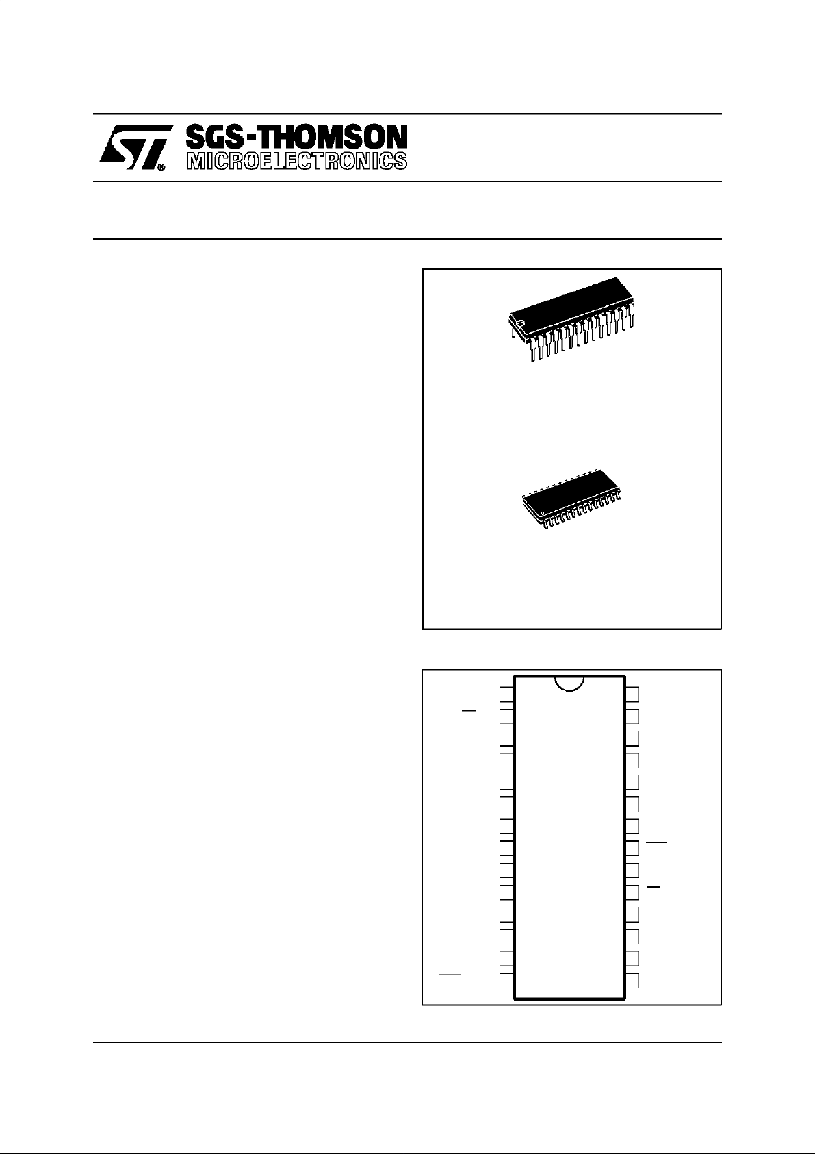
28 PINDIP &SO PACKAGE
STV5347
STV5347/H - STV5347/T
WITH 4 INTEGRATEDPAGES
DIP28
(PlasticPackage)
ORDER CODE :
STV5347 West European
STV5347/H East European
STV5347/T Turkish& European
SO28
(PlasticPackage)
ORDER CODE :
STV5347D West European
STV5347D/H East European
STV5347D/T Turkish & European
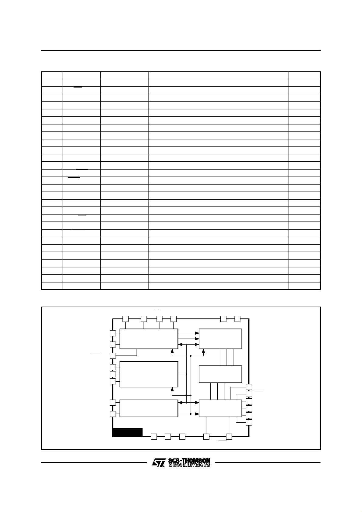
PIN CONNECTIONS
DESCRIPTION
The STV5347 teletext decoder is computer-controlled.It can storeeither 4 teletext pages without
ghostrow,or 2 teletextpageswithghostrows.Data
slicing and capturing extracts the teletext informationembedded in thecompositevideo signal. ControlisaccomplishedviaatwowireserialI
Chip address is 22h. Internal ROM provides a
character set suitable to display text using up to
sevennationallanguages.Hardware andsoftware
features allow selectable master/slave synchronizationconfigurations.The STV5347also supports
facilities for reception and display of current level
protocoldata.
June 1997
2
C bus.
CVBS
MA/SL
V
DDA
POL
STTV/LFB
FFB
V
SSD
RGB REF
BLAN
COR
1
2
3
4
5
6
7
8
R
9
G
10 19
B
11 18
12 17
13 16
14 15ODD/EVEN
28
27
26
25
24
23
22
21
20
CBLK
TEST
V
SSA
V
SSO
XTI
XTO
V
DDD
VCR/TV
RESERVED
DV
L23
SDA
SCL
Y
5347-01.EPS
1/22
Page 2
STV5347 - STV5347/H - STV5347/T
PIN DESCRIPTION
o
Pin N
1 CVBS Input Composite VideoSignal Inputthrough Coupling Capacitor 9
2 MA/SL Input Master/Slave Selection Mode 11
3V
4 POL Input STTV / LFB /FFB PolaritySelection 12
5 STTV/LFB Output / Input Composite Sync Output,Line FlybackInput 15
6 FFB Input Field Flyback Input 12
7V
8 R Output Video Red Signal 13
9 G Output Video Green Signal 13
10 B Output Video Blue Signal 13
11 RGBREF Supply DC Voltage to define RGB High Level 13
12 BLAN Output Fast BlankingOutput TTLLevel 15
13 COR Output Open DrainContrast Reduction Output 15
14 ODD/EVEN Output 25Hz Output Field synchronized for non-interlaced display 15
15 Y Output Open Drain Foreground Information Output 15
16 SCL Input Serial Clock Input 16
17 SDA Input/ Output Serial Data Input/Output 17
18 L23 Output Line 23 Identification 15
19 DV Output VPS Data Valid 15
20 RESERVED Test To be connected to V
21 VCR/TV Input PLL TimeConstant Selection 15
22 V
23 XTO Crystal Output Oscillator Output 13.875MHz 14
24 XTI CrystalInput Oscillator Input 13.875MHz 14
25 V
26 V
27 TEST Test Grounded to V
28 CBLK Input / Output Toconnect Black Level StorageCapacitor 28
Symbol Function Description Figure
DDA
SSD
DDD
SSO
SSA
Analog Supply +5V -
Ground Digital Ground -
througha resistor 15
SSD
Digital Supply +5V -
Ground Oscillator Ground Ground Analog Ground -
SSA
11
5347-01.TBL
BLOCKDIAGRAM
2/22
CVBS
CBLK
VCR/TV
XTI
XTO
V
SSO
SCL
SDA
1
28
21
24
23
25
16
17
STV5347
MA/SL
CLAMPING
SYNCHRONIZING
DATAEXTRACTION
OSCILLATOR
FREQUENCY
SYNTHETIZER
TIME BASE
2
I C BUS
INTERFACE
726 1411
V
V
SSD
POLFFBSTTV/LFB
Data
Clock
27
TES T RGB REF
SSA
V
DDD
DATADECODING
DATA
PROCES SING
Address
Data
CTRL
4 PAGE
MEMORY
Data
Address
CTRL
DISP LAY
INTERFACE
ODD/EVEN
V
DDA
3225624
BLAN
12
COR
13
RED
8
GREEN
9
BLUE
10
Y
15
5347-02.EPS
Page 3
STV5347 - STV5347/H - STV5347/T
ABSOLUTEMAXIMUM RATINGS
Symbol Parameter Value Unit
V
∆V
T
V
T
DD
V
oper
stg
O
DD
Positive Supply Voltageon V
Input Voltage (any input) - 0.3, VDD+ 0.5 V
I
Output Voltage (any output) - 0.3, VDD+ 0.5 V
Difference between V
DDD,VDDA
Operating Ambient Temperature 0, + 70
Storage Temperature - 40, +150
DDD
and V
DDA
- 0.3, 6.0 V
0.25 V
o
C
o
C
5347-02.TBL
ELECTRICAL CHARACTERISTICS
= 5V,VSS= 0V,TA=25oC)
(V
DD
Symbol Parameter Min. Typ. Max. Unit
SUPPLIES
V
I
DDD
I
DDA
DD
Supply Voltage 4.75 5 5.25 V
V
Pin Supply Current 30 mA
DDD
V
Pin SupplyCurrent 5 mA
DDA
INPUTS
CBLK
I
BLKO
I
BLKI
Source Current (V
Sink Current (V
CBLK
CBLK
=2V,V
=2V,V
CVBS
= 0V) 80
CVBS
= 1V)) - 10
CVBS
CVBSI Video Input Amplitude (peak to peak) 1 V
CVBSC InputCapacitance 10 pF
t
SYNC
V
CLAMP
I
CLPH
I
CLPL
Delay from CVBS to TCS Output from STTV Pin 200 ns
Clamping Level at Synchro Pulse 0 mV
High Level Clamp Current (CVBS = V
Low Level Clamp Current (CVBS= V
+ 1V) 5
CLAMP
- 0.3V) - 400 µA
CLAMP
MA/SL, POL, LFB, FFB, VCR/TV
V
IL
V
IH
I
IL
C
Input Voltage Low Level - 0.3 + 0.8 V
Input Voltage High Level 2 V
Input Leakage Current (VI= 0 to V
Input Capacitance 10 pF
I
) - 10 + 10
DDD
DD
SCL, SDA
V
V
I
f
SCL
t
R,tF
C
IL
IH
IL
Input Voltage Low Level - 0.3 + 1.5 V
Input Voltage High Level 3 V
Input Leakage Current (VI= 0 to VDD) - 10 + 10 µA
Clock Frequency (SCL) 100 kHz
Input Rise and Fall Time(10 to 90%) 2
Input Capacitance 10 pF
I
DD
RGB REF
V
I
I
Input Voltage - 0.3 V
I
Input Current 50 mA
DD
A
µ
A
µ
A
µ
V
A
µ
V
s
µ
V
5347-03.TBL
3/22
Page 4
STV5347 - STV5347/H - STV5347/T
ELECTRICALCHARACTERISTICS -
=5V, VSS= 0V,TA=25oC (continued)
V
DD
Symbol Parameter Min. Typ. Max. Unit
OUTPUTS
RGB
V
V
C
t
R,tF
Output Low Voltage (IOL= 2mA) 0.4 V
OL
Output High Voltage (IOH= -2mA, RGB REF = VDD/2) RGB REF - 0.5 RGB REF V
OH
Load Capacitance 50 pF
L
Rise and Fall Time (10 to 90%) 20 ns
BLAN
V
V
C
t
R,tF
Output Low Voltage (IOL= 2mA) 0 0.4 V
OL
Output High Voltage (IOH= -0.2mA) VDD- 0.5 V
OH
Load Capacitance 50 pF
L
Rise and Fall Time (10 to 90%) 20 ns
ODD/EVEN, STTV,L23, DV
V
V
C
t
R,tF
COR AND Y(with Pull up to V
V
C
I
OLL
Output Low Voltage(IOL= 2mA) 0 0.5 V
OL
Output High Voltage (IOH= -0.2mA) VDD- 0.8 V
OH
Load Capacitance 50 pF
L
Rise and Fall Time (10 to 90%) 20 ns
)
DDD
Output Low Voltage (IOL= 2mA) 0 0.5 V
OL
Load Capacitance 25 pF
L
t
Fall Time (RL= 1.2kΩ,V
F
- 0.5Vto 1.5V) 50 ns
DDD
Output Leakage Current -10 +10 µA
DD
SDA
V
C
Output Low Voltage (IOL= 3mA) 0 0.5 V
OL
t
Fall Time (3.0 to 1.0V) 200 ns
F
Load Capacitance 400 pF
L
CRYSTALOSCILLATOR
XTI, XTO
f
R
XTAL
BIAS
C
Crystal Frequency 13.875 MHz
Internal Bias Resistance 0.4 1 3 M
Input Capacitance 7pF
I
TIMING
SERIAL BUS(referred to V
=3V,VIL= 1.5V)
IH
Clock :
t
LOW
t
HIGH
t
SU, DAT
t
HD,DAT
t
SU, STO
t
BUF
t
HD, STA
t
SU,STA
Low Period
●
High Period
●
Data Set-up Time 250 ns
Data Hold Time 170 ns
Stop Set-upTime fromClock High 4
Start Set-up Time followinga Stop 4
Start Hold Time 4 µs
Start Set-up Time followingClock Low to High Transition 4 µs
4
4
µs
µ
µ
V
Ω
s
s
5347-04.TBL
4/22
Page 5
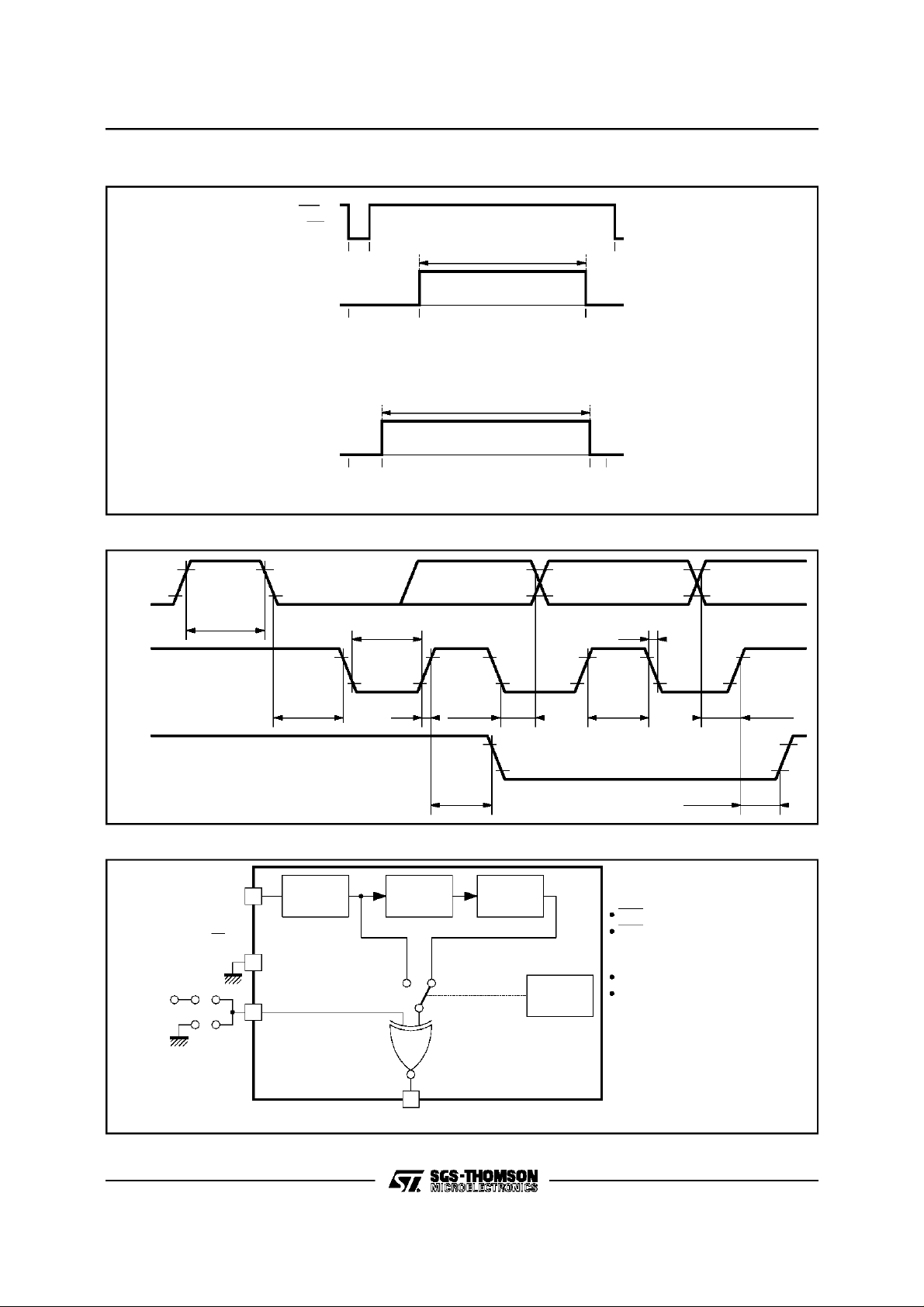
Figure 1 : DisplayOutput Timing
LSP
(TCS)
R.G.B.Y
(1)
STV5347 - STV5347/H - STV5347/T
µs
0 4.66 64
40
Figure 2 : SerialBus Timing
SDA
t
BUF
SCL
t
SDA
R.G.B.Y
(1)
HD,STA
0
16.67 56.67
(a) LINE RATE
all timingsin µs
lines 42 to 291 inclusive
(and 355 to 604 inclusiveinterlaced)
0
(b) FIELD RATE
t
LOW
t
t
R
HD,DAT
31229141
line numbers
t
HIGH
5347-03.EPS
t
F
t
SU,DAT
t
VIH=3V,VIL=1.5V
SU,STA
Figure3 : MasterSynchronizationMode - HardwareConfiguration
Synchro
+5V
MA/SL
POL
1
Extractor
2
VCS
R
4
Line PLL Line PLL
=”0”
1D2
STTV
TCS
R1D2=”1”
Bit R
1D2
Control
I2C
t
SU,STO
Output signal on STTV Pin :
POL grounded
VCS when R
TCS when R
POL to V
DD
VCS when R
TCS when R
1D2
1D2
1D2
1D2
=0
=1
=0
=1
5347-04.EPS
5347-05.EPS
5/22
Page 6
STV5347 - STV5347/H - STV5347/T
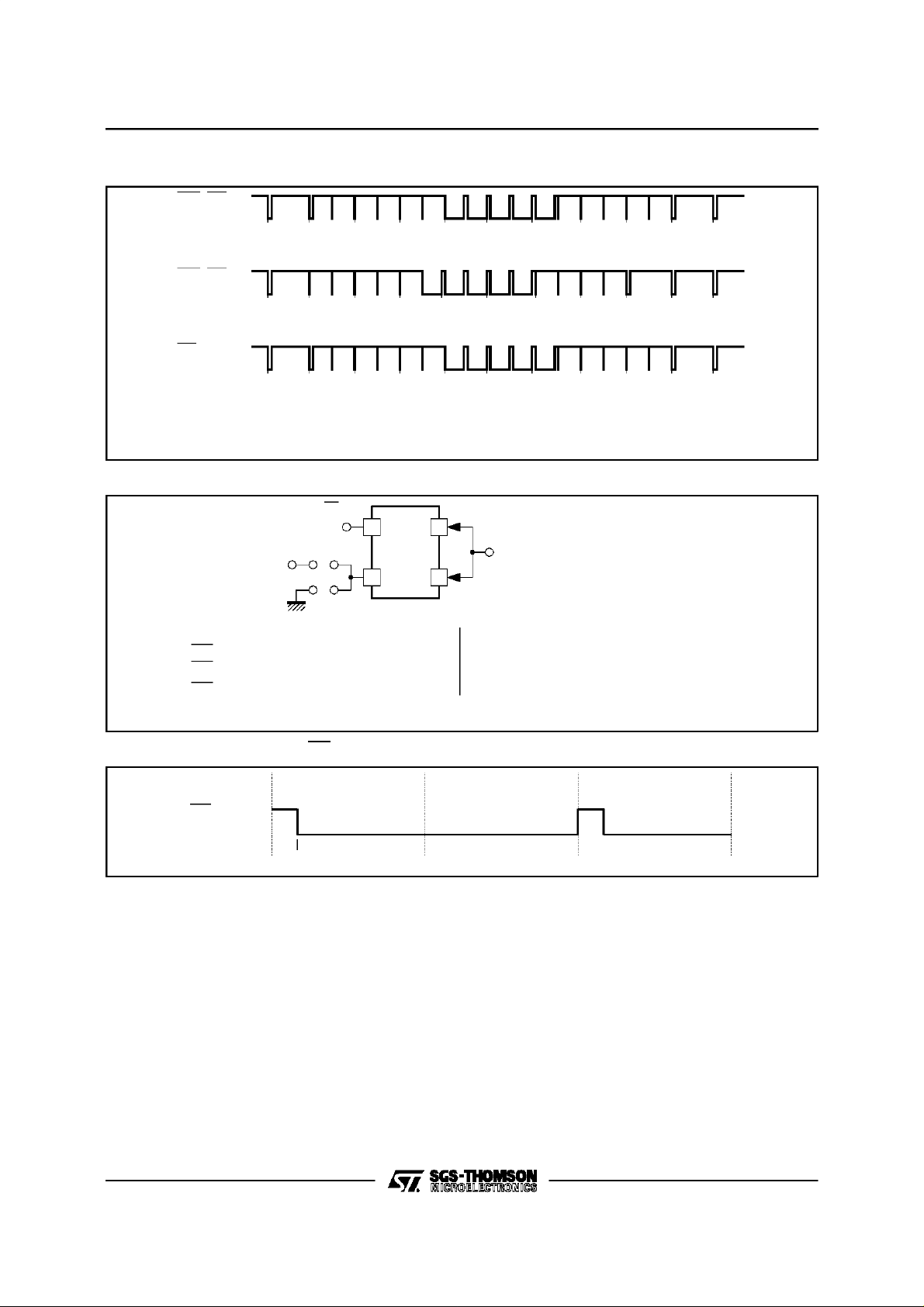
Figure4 : MasterSynchronizationMode - DeliveredCompositeSynchronizationSignal
VCS, TCS
(interlaced)
621
622
(308)
(309)
VCS, TCS
(interlaced)
309 310 311 312 313 314
TCS
(non-interlaced)
308 309 310 311 312 1 2 3 4 5 6
The numberpositions indicate the end of lines.
Internal signals:
- VCS compositesynchro from CVBSsignal,
- TCS Teletextcompositesynchro.
Figure5 : SlaveSynchronizationMode
623
(310)
624
(311)
625
(312)
12 3456
315
316
317
(1)
(2)
(3)
(4)
318
(5)
319
(6)
5347-06.EPS
MA/SL
+5V
+5V
POL grounded,Inputs Signals :
are
LFB line flybacksynchro onPin 5
FFB field flyback synchro on Pin 6
or SCS synchro composite signalon Pins 5 and 6
Note : R
and R1D1must be setto 1.
1D0
Figure6 : DataValidTiming (DV)
DV for
VPS Data
Line 16
25
POL
4
Field 0
LFB
SCS
6
FFB
POL to V
, InputsSignals :
DD
are LFB line flyback synchro on Pin 5
FFB field flyback synchroon Pin 6
or SCS synchro composite signalon Pins 5 and 6
Field1 Field0
5347-07.EPS
5347-08.EPS
6/22
Page 7
FUNCTIONAL DESCRIPTION
I - Displayable Page MemoryMap
The organization of a page-memory is shown in
Figure7.
Thedisplay areaconsists of25 rowsof 40 characters per row.
Theorganization isas follows:
- Row zero containsthe pageheader :
• The first seven characters (0 - 6) are used for
messagesregarding the operationalstatus.
• The eighthcharacteris an alphanumericcontrol
character either“white” or “green” defining the
“search” status of the page. When it is “white”
the operational state is normal and the header
appears white ; when it is “green” the opera-
Figure7 : Page Memory Organization
Fixed characters
7 Status
Characters
Alphanumerics white
for normal,
green on search
24 characters from page header
rolling on page search
STV5347 - STV5347/H - STV5347/T
tional state corresponds to the “search mode”
and the header appearsgreen.
• The following twenty-four characters give the
headerof therequested pagewhen thesystem
is in searchmode.
• Thelast eightcharactersdisplaythetimeof day.
- Row number twenty-four is used by the microprocessor for the display of information, or used
to display X/24 colored key data according to
R0D7 bit.
- Row twenty-five comprises ten bytes of control
data concerningthe received page (see Table 1)
and fourteenfreebytes whichcan be usedby the
microprocessor.
8 scrolling
time characters
ROW
17248
MAIN PAGE DISPLAY AREA
row free for status (R0D7 = 0) or packet X/24 (R0D7= 1)
10 14
0
1
2
3
4
5
6
7
8
9
10
11
12
13
14
15
16
17
18
19
20
21
22
23
24
25
10 bytes for received
page information
14 bytes free
for use byµC
5347-09.EPS
7/22
Page 8

STV5347 - STV5347/H - STV5347/T
FUNCTIONAL DESCRIPTION(continued)
II - GhostRow Storage Organization
Row Address
of Stored Data
0 0000
1 0001
2 0010
3 0011
4 0100
5 0101
6 0110
7 0111
8 1000
9 1001
10 1010
11 1011
12 1100
13 1101
14 1110
15 0 0 1 0 X / 28 Conditional access
16 0000
17 0001
18 0100
19 0101
20 X / 24 Page extension stored here ifR0D7 = 0
21 X / 25 Page extension
22 0 0 0 0 X /28 Color definition
23 X X X X 8 /30 * * Broadcasting service data packet
24 0 0 0 1 X/28 Character set designation
25 ** Notused
* Packet 8/30 storage : 8/30/0,1 : chapter 4, row23
** See table 2 for VPS data storage in chapter 5
Table 1 : Row 25 Received PageControl DataFormat
Designation
Code
Row (Packet)
Number
X /26 Enhanced display facilities
X/27
8/30/2,3 : chapter 5, row23
8/30/4 to 15 : chapter6, row23
Function
Editorial
Linked pages
Composition
Page relateddata
stored inchapter
corresponding to
level 1data,
i.e. For 0 goes in 4
“1 ” “5
”2 “ ”6
“3 ” “7
5347-05.TBL
D0 PU0 PT0 MU0 MT0 HU0 HT0 C7 C11 MAG0 0
D1 PU1 PT1 MU1 MT1 HU1 HT1 C8 C12 MAG1 0
D2 PU2 PT2 MU2 MT2 HU2 C5 C9 C13 MAG2 0
D3 PU3 PT3 MU3 C4 HU3 C6 C10 C14 0 0
D4 HAM HAM HAM HAM HAM HAM HAM HAM FOUND 0
D5 000000000PBLF
D6 0000000000
D7 0000000000
COLUMN 0 1 23456789
Page number : - MAG = magazine,PU = page units, PT = page tens.
Page sub-code : -MU = minutesunits, MT= minutes tens, HU = hours units, HT = hours tens.
PBLF = page being looked for, FOUND = low forpage found, HAM = hamming error inbyte, C4-14 = control bits.
8/22
5347-06.TBL
Page 9

STV5347 - STV5347/H - STV5347/T
FUNCTIONAL DESCRIPTION
III - VPS DATA
(seeTable2)
VPSdata are storedin row25 chapter5 asshown
in Table2 when VPSenable bit(D4 of R8 register)
is set. VPS data bits are decoded and stored in a
receivedareawithbiphaseerrorbit.8/30/2dataare
storedas received(without hamming decoding)in
Row23 chapter5 accordingtoTable2. 8/30packet
and VPS data decodingis the responsibilityof the
controlsoftware. Thedecoder simply storestransmitteddata.
2
C Bus Register Map
IV- I
RegistersR0 to R10 are write only whilst R11Ais
a read/writeandR11Bis read only.
Theautomatic succession on a byte bybyte basis
is indicatedby the arrowsin Table3.
In the normaloperatingmode TB shouldbe set to
logic level 0.
(continued)
(seeTable3)
Afterpower-up the contentsof the registersare as
follows: allbitsin registersR0 toR11Aare cleared
to zero with the exception of bits D0 and D1 in
registersR5 and R6 which are set to logicalone.
After power-upall the memorybytes are preset to
hexadecimalvalue 20H(space)with theexception
of the byte correspondingto row 0 of column 7 of
chapter 0 which is set to the value corresponding
to “alphawhite” hexadecimalvalue 07H.
In 4 pages mode, R1D4(ghost row enable) is set
to ’0’. In this mode, the X/24, X/26, X/27, X/28
packets of the selectedpages,and the 8/30packets, are not stored.
In 2 pages mode, R1D4(ghost row enable) is set
’1’. In this mode two displayable pages can be
storedinchapter0and1,andthe ghostrowsofthe
selected pages, and the 8/30 packets, are stored
in chapter4 and 5.
Table2 : PDCData Storage inChapter 5
Column 012345678910111213141516171819
8/30/2(Row23) D InitialPage b13 b14 b15 b16 b17 b18 b19 b20 b21 b22 b23 b24 b25
VPS (Row 25) Received Page Information B11 B12 B13 B14 B15
Column 20 21 22 23 24 25 26 27 28 29 30 31 32 33 34 35 36 37 38 39
8/30/2(Row23) Status Display
VPS (Row 25) B4 B5
Table3 : RegisterSpecification
D7 D6 D5 D4 D3 D2 D1 D0
X24
POSITION
(1) 7 +P/
(1) BANK
(1) (1) (1) PRD4 PRD3 PRD2 PRD1 PRD0 R3 Page request data
(1) (1) (1) (1) (1) A2 (2) A0 R4 Display chapter
BKGND
OUT
BKGND
OUT
STATUS
ROW
BTM/TOP
(1) (1) (1) VPS
(1) (1) (1) R4 R3 R2 R1 R0 R9 Active row
(1) (1) C5 C4 C3 C2 C1 C0 R10 Active column
D7
(R/W)
60Hz 0 0 0 0 0 DATA
(1) Reservedregisterbits : must be set to 0
(2) Inactive
FREE
RUNNING
PLL
8 BIT
SELECT
A2
BKGNDINCOR
BKGNDINCOR
CURSOR
ON/OFF
D6
(R/W)D5(R/W)
(1) DISABLE
ACQ.
ON/OFF
(2) ACQ.
OUT
OUT
CONCEAL/
REVEAL
ROLLING
HEADER
GHOST
ROW
ENABLE
CCT
A0
COR
IN
COR
IN
TOP/
BOTTOM
ENABLE
D4
(R/W)D3(R/W)D2(R/W)D1(R/W)D0(R/W)
(1) EVEN
DEW/
FULL
FIELD
TB START
TEXT
OUT
TEXT
OUT
SINGLE/
DOUBLE
HEIGHT
CLEAR
MEM.
OFF
TCS
ON
COLUMN
SC2
TEXTINPON
TEXTINPON
BOX ON24BOX ON
A2 (2) A0
(1) SEL 11B
T1 T0
START
COLUMN
SC1
OUT
OUT
1-23
QUAL
START
COLUMN
SC0
PON
IN
PON
IN
BOX ON
0
V
CS
QUAL
↵
↵
↵
↵
↵
↵
↵
↵
↵
R0 Mode 0
R1 Mode 1
R2 Page request address
R5 Display control (normal)
Display control
R6
(newsflash / subtitle)
R7 Display mode
R8 Active chapter
R11A Active data
R11B Status
5347-11.TBL
5347-07.TBL
9/22
Page 10

STV5347 - STV5347/H - STV5347/T
FUNCTIONAL DESCRIPTION(continued)
2
IV - I
C Bus Register Map (continued)
IV.1- Registers Functions
Register Function Bit(s) Description
SEL 11B(D0) Selection of register 11B(D0 = 1) or 11A(D0 = 0)
R0
Address
00H
R1
Address
01H
R2
Address
02H
R3
Address
03H
R4
Address
04H
R5
Address
05H
R6
Address
06H
R11 adressing and
pin functions control
Operating mode
controls
Addressing
information for
a page request
Data relative to the
requested page
(see Table 3)
Selection of one of
eight pages to
display
Display controlfor
normal operation
Display controlfor
news-flash subtitle
generation
EVEN OFF (D2) Control of ODD/EVEN pin: EVEN signal output
DISABLE ROLLING
HEADER
FREE RUNNING
PLL(D6)
X/24 POSITION (D7) D7 = 0, packet X/24 stored to chapter 4 to 7/row 20
T1 (D1) T0 (D0)
00
01
10
11
TCS ON (D2) Master Mode (MA/SLPin 2 = 0)
DEW / FULLFIELD
(D3)
GHOST ROW
ENABLE (D4)
ACQUISITION
ON / OFF (D5)
7bits +parity or 8 bits
without parity (D6)
SC0, SC1, SC2
(D0, D1, D2)
TB (D3) Test bit equal to “0” in the normal working mode.
A0, A1(D4, D5) Address a group of four consecutive pages currently used
A2 (D6) Addressof one ofthe two groups of four pages for
PRD0 - PRD4
(D0 - D4)
A0, A1, A2
(D0, D1, D2)
PON (D0, D1) Picture on (IN: D0, OUT:D1)
TEXT (D2, D3) Texton (IN:D2, OUT:D3)
COR (D4, D5) Contrast reduction on (IN: D4, OUT:D5)
BKGND (D6, D7) Background color on (IN: D6, OUT:D7)
IN / OUT Enable inside/outside the box
See R5 See R5
(D2 = 0) or grounded (D2 = 1)
D4 = 1, Disable rolling header
D4 = 0, Normaloperation
D6 = 0, PLLlocks on line frequency
D6 = 1, toforce free running mode
D7 = 1, packetX/24 stored to chapter 0to 3/row 24
Character display line control :
312.5/312.5 line MIX - mode with interlace
312/313 line TEXT -mode without interlace
312/312 line Terminal mode without interlace
External synchronization. SCS mode (scan field synchro)
case POLPin 4 = 0
D2 = 0, Pin 5 = VCS
D2 = 1, Pin 5 = TCS
Slave Mode (MA/SL Pin 2 = V
No effect
Selection of field flybackmode or fullchannel mode
(D3 = 1) for recovering of Teletextdata.
Selection of ghost row mode (D4 = 1)
Control of acquisition operation (D5 = 0 enables
acquisition)
Selection of received data format either 7 bits withparity
(D6 = 0) or 8 bits without parity (D6 = 1).
Address the first column of the on chip pagerequest RAM
to be written.
for data acquisition.
acquisition in normal mode.
Written data in thepage request RAM, starting with the
columns addressed by SC0,SC1,SC2.
Chapter selection.
DD
)
5347-08.TBL
10/22
Page 11

STV5347 - STV5347/H - STV5347/T
FUNCTIONAL DESCRIPTION
2
C Bus Register Map
IV - I
(continued)
(continued)
IV.1- Registers Functions (continued)
Register Function Bit(s) Description
BOX ON 0, 1-23,24
(D0, D1, D2)
TOP / BOTTOM
R7
Address
07H
R8 Memory access
R9 to R11A
Address
08H to0BH*
R11B
Address
0BH*
* Readingof R11Aor R11Bis determinedby register 0, bit D0.However,write operationis a lways performed on R11A register.
Display mode
Active row address (R9), activecolumn address (R10).
Data containedin R11Aread (written) from (to) memory by microprocessor via I
Status
Single/ Double Height
(D4/D3)
Conceal / Reveal (D5) Conceal Reveal Function
Cursor ON/OFF (D6) Cursor position given by row/column value of R9/R10
STATUSROW
BTM / TOP (D7)
VPS Enable (D4) D4 = 1Enable VPS acquisition and DV signal output.
Clear Memory (D3) D4 = 1Clear memory.
Chapter Address
(D2, D1, D0)
VCS QUAL(D0) Good VCS quality signal detected (D0 = 1).
DATAQUAL (D1) Good TELETEXT signal (D1 = 1).
50/60Hz (D7) If D1 = 0 frame frequencyis 50Hz (onlyvalid with good
The “boxing” function is enabled on row 0,1-23 and 24 by
D0, D1 and D2 set to one.
X0 = Normal
01 = double height Rows 0 to 11
11 = double height Rows 12to 23
The row 24 is displayedbefore the “Main text Area” (lines
0-23) or after (D7 =0).
Chapter selectedwith A2A1A0 (D2,D1, D0)R4.
Chapter selection
Bad VCS quality signal detected(D0 = 0).
Bad TELETEXTsignal (D1 = 0).
VCS)
2
C.
5347-09.TBL
Table4 :
START
COLUMN
0 Do care magazine HOLD MAG2 MAG1 MAG0
1 Do care page tens PT3 PT2 PT1 PT0
2 Do care page units PU3 PU2 PU1 PU0
3 Do care hours tens X X HT1 HT0
4 Do care hours units HU3 HU2 HU1 HU0
5 Do care minutes tens X MT2 MT1 MT0
6 Do care minutes units MU3 MU2 MU1 MU0
The abbreviations havethesame significance as in Table 1withthe exception of the “DO CARE” entries.It is only when this bit is “1”
that the corresponding digitis taken into consideration on page request. For example,a page defined as ”normal” or one defined as
“timed” may be selected.
If “HOLD” islow the page is held. The addressing of successive bytes via theI
RegisterR3
PRD4 PRD3 PRD2 PRD1 PRD0
2
C is automatic.
V - CharacterSets
The completecharacter set with 8-bit decoding is
given in Table5.
Characters in columns 0 and 1 are normally displayedasblanks.Blackdots representthe character shape whereas white dots represent the
background.
Eachcharactercan beidentified by apair of corre-
sponding row and column integers : for example
the character“3” may be indicatedby 3/3.
Arectangle may be representedas follows:
The characters8/6, 8/7, 9/5,9/7 are used as spe-
cial characters,alwaysin conjunctionwith 8/5.
The 13 national characters are placed in columns
with bit 8 = 0.
5347-10.TBL
11/22
Page 12

STV5347 - STV5347/H - STV5347/T
FUNCTIONAL DESCRIPTION(continued)
Table5 : STV5347Complete Character Set (with 8bit codes) - West European Languages
1
1
1
1
0
1
1
1
1
0
13 14 15
1
1
0
0
1
1
1
0
912
0
1
0
0
0
1
7a 8
1
1
1
0
0
0
0
0
or 1
0
0
or 1
0b
0
0
8
BIT
Case usingC12 C13 C14 = 001(German Set)
* These control charactersare reserved for compatibilitywith otherdata codes.
** Thesecontrol charactersare presumedbefore eachrow begins
1
1
0
1
0
1
1
0
1
0
1
0
1
0
0
0
0
0
b7b6b
7
0
6 6a
1
5
0
4
1
3a
1
3
0
2a
0
2
display
conceal
flash
8
**
continuous
**
steady
9
graphics
1
10
graphics
0
alphanumerics
column
row
5
1
b
2
b
3
b
4
S
b
black
black
0
000
0
red
graphics
green
graphics
graphics
yellow
blue
graphics
graphics
magenta
cyan
graphics
graphics
white
**
red
alphanumerics
alphanumerics
1
green
alphanumerics
2
yellow
3
blue
alphanumerics
alphanumerics
4
5
magenta
cyan
alphanumerics
alphanumerics
6
7
white
1
010001101000101011110001001101010111100110111101111
0000
110
0
graphics
separated
**
endbox
10
*
ESC
start box
11
**
black
**
normal
12
**
new
background
height
double
13
background
height
*
hold
SO
14
**
graphics
*
release
graphics
SI
15
5347-10.EPS
12/22
Page 13

STV5347 - STV5347/H - STV5347/T
FUNCTIONAL DESCRIPTION(continued)
Table6 : STV5347/HCompleteCharacter Set(with 8 bit codes) - EastEuropeanLanguages
1
1
1
1
0
1
1
1
1
0
1
1
0
0
1
1
1
0
0
11
0
0
0
1
1
1
0
0
1
1
0
1
0
1
0
0
0
1
0
0
1
0
0
0
1
0
0
1
0
0
1
0
1
0
0
0
0
0
S
33a4 5 66a77a8 912131415
22a
12
column
row
1
b
2
b
3
b
4
b
black
graphics
graphics
black
alphanumerics
alphanumerics
0
1
1000
0000
red
red
green
graphics
graphics
green
alphanumerics
alphanumerics
2
3
0010
0011
yellow
yellow
blue
graphics
graphics
blue
alphanumerics
alphanumerics
4
5
0100
0101
magenta
magenta
cyan
graphics
cyan
alphanumerics
60110
or 1
0
or 1 0
0b
0
0
8b7b6b5
BIT
Case usingC12 C13 C14 = 001(Rumanian Set)
* These control charactersare reserved for compatibilitywith otherdata codes.
** Thesecontrol charactersare presumedbefore eachrow begins
white
graphics
**
white
alphanumerics
7
0111
display
conceal
flash
8
1000
**
continuous
**
graphics
steady
9
1001
graphics
separated
**
end box
10
1010
*
ESC
start box
11
1011
**
black
**
normal
12
1100
**
new
background
height
double
13
1101
hold
background
*
SO
height
14
1110
**
graphics
*
release
graphics
SI
15
1111
5347-??.EPS
13/22
Page 14

STV5347 - STV5347/H - STV5347/T
FUNCTIONAL DESCRIPTION(continued)
Table7 : STV5347/TCompleteCharacter Set(with 8 bit codes) - Turkish European Languages
1
1
1
1
0
1
1
1
1
0
1
1
0
0
1
1
1
0
0
11
0
0
0
1
1
1
0
0
1
1
0
1
0
1
0
0
0
1
0
0
1
0
0
0
1
0
0
1
0
0
1
0
1
0
0
0
0
0
S
33a4 5 66a77a8912131415
22a
12
column
row
1
b
2
b
3
b
4
b
black
graphics
black
alphanumerics
0
0000
red
graphics
red
alphanumerics
1
1000
green
graphics
graphics
green
alphanumerics
alphanumerics
2
0010
yellow
graphics
yellow
alphanumerics
3
0011
blue
graphics
blue
alphanumerics
4
0100
graphics
magenta
magenta
alphanumerics
5
6011078
0101
cyan
cyan
or 1
0
or 1 0
0b
0
0
8b7b6b5
BIT
Case usingC12 C13 C14 = 001(German Set)
* These control charactersare reserved for compatibilitywith otherdata codes.
** Thesecontrol charactersare presumedbefore eachrow begins
white
graphics
**
white
alphanumerics
0111
display
conceal
flash
1000
**
continuous
**
steady
9
1001
graphics
**
graphics
separated
end box
10
1010
*
ESC
start box
11
1011
**
black
background
**
height
normal
12
1100
**
new
double
13
1101
hold
background
*
SO
height
14
1110
**
graphics
*
release
graphics
SI
15
1111
5347-??.EPS
14/22
Page 15

FUNCTIONAL DESCRIPTION(continued)
The basic set of the 96 characters is shown in
Table 8.The location of the 13 nationalcharacters
STV5347 - STV5347/H - STV5347/T
are shown in Table 8 whilst full national character
sets are depicted in Tables9, 10 and 11.
Table8 :
Basiccharacterset.
2/0
2/1
2/2
2/3
2/4
2/5
2/6
2/7
National
Character
National
Character
3/0
3/1
3/2
3/3
3/4
3/5
3/6
3/7
4/0
4/1
4/2
4/3
4/4
4/5
4/6
4/7
National
Character
5/0
5/1
5/2
5/3
5/4
5/5
5/6
5/7
6/0
6/1
6/2
6/3
6/4
6/5
6/6
6/7
Nation al
Character
7/0
7/1
7/2
7/3
7/4
7/5
7/6
7/7
2/8
2/9
2/10
2/11
2/12
2/13
2/14
2/15
3/8
3/9
3/10
3/11
3/12
3/13
3/14
3/15
4/8
4/9
4/10
4/11
4/12
4/13
4/14
4/15
5/8
5/9
5/10
5/11
5/12
5/13
5/14
5/15
National
Character
National
Character
National
Character
National
Character
National
Character
6/8
6/9
6/10
6/11
6/12
6/13
6/14
6/15
7/8
7/9
7/10
7/11
7/12
7/13
7/14
7/15
National
Character
National
Charact er
National
Charact er
National
Character
5347-11.EPS
15/22
Page 16

STV5347 - STV5347/H - STV5347/T
FUNCTIONAL DESCRIPTION(continued)
Table9 : STV5347CharacterSet - West European Languages
CHARACTER POSITION (COLUMN/ROW)
2/3 2/4 4/0 5/11 5/12 5/13 5/14 5/15 6/0 7/11 7/12 7/13 7/14
PHCB (1)
000
001
001
011
100
FRENCH
101
SPANISH
C12 C13 C14
LANGUAGE
ENGLISH
GERMAN
SWEDISH
ITALIAN
Note 1 : Where PHCB are the Page Header Controlbits. OtherCombinationsdefault to English. Only the abovec haracterschange with thePHCB. All others
charactersin the basicset areshown in Table 5.
5347-12.EPS
16/22
Page 17

FUNCTIONAL DESCRIPTION(continued)
Table 10 : STV5347/H Character Set -
East EuropeanLanguages
STV5347 - STV5347/H - STV5347/T
Table11 : STV5347/T Character Set-
Turkish European Languages
CHARACTER POSITION (COLUMN/ROW)
PHCB (1)
Note1 :
2/3 2/4 4/0 5/11 5/12 5/13 5/14 5/15 6/0 7/11 7/12 7/13 7/14
1
011
000
001
GERMAN
001
SWEDISH
C12 C13 C14
LANGUAGE
POLISH
Where PHCB are thePage Header Controlbits.Other
Combinations default to German. Only the abovecharacters
change with the PHCB.All others charactersin the basic set are
shown in Table7.
10
SERBO-CROAT
CZECHOSLOVAK
CHARACTER POSITION (COLUMN/ROW)
2/3 2/4 4/0 5/11 5/12 5/13 5/14 5/15 6/0 7/11 7/12 7/13 7/14
PHCB (1)
11
RUMANIAM 1
5347-??.EPS
Note 1 :
C12 C13 C14
LANGUAGE
WherePHCB are the Page Header Controlbits. Other
Combinations default to Turkish. Only the above characters
changewith the PHCB. All otherscharactersin the basicset are
shownin Table7.
000
ENGLISH
001
GERMAN
01
1
TURKISH
011
ITALIAN
100
FRENCH
101
SPANISH
17/22
5347-??.EPS
Page 18

STV5347 - STV5347/H - STV5347/T
FUNCTIONAL DESCRIPTION(continued)
Figure8 : CharacterFormat
Alphanumerics and
Graphics ’space’
character
2/0
Contiguous
graphics character
7/6
Alphanumerics
character
2/13
Separated
graphics character
7/6
Alphanumerics or
blast-through
alphanumerics
character 4/8
Separated
graphics character
7/15
Background
Color
Alphanumerics
character
7/15
Contiguous
graphics character
7/15
Display
==
Color
5347-17.EPS
18/22
Page 19

I/O PIN ELECTRICAL SCHEMATICS
Figure9 : Analog1 (CVBS)
V
DDA
CVBS 250
Ω
1
V
SSA
Figure11 : InputA
STV5347 - STV5347/H - STV5347/T
Figure10 : Analog2 (CBLK)
CBLK 250Ω
28
5347-18.EPS
Figure12 : InputD
V
DDA
V
SSA
5347-19.EPS
Pins 2, 27
MA/SL,TEST
Figure13 : PRGB
V
DDD
Figure15 :
INOUT
RGB REF
11
Pins
8, 9,10
R, G,B
450Ω
V
SSA
V
DDA
450Ω
V
SSD
Pins 4,6
POL, FFB
5347-20.EPS
Figure14 : PXTAL
XTI
5347-22.EPS
450Ω
V
V
V
SSD
SSD
DDD
V
DDD
5347-21.EPS
750kΩ
XTO450Ω
450Ω
2324
5347-23.EPS
Pins 5, 12,13, 14,
15, 18, 19, 20, 21
STTV/LFB, BLAN, COR,
ODD/EVEN, Y, L23,
DV, RESERVED, VCR/TV
V
V
450
SSD
DDD
Ω
5347-24.EPS
19/22
Page 20

STV5347 - STV5347/H - STV5347/T
I/O PIN ELECTRICAL SCHEMATICS(continued)
Figure16 : PSCL
Figure17 : PSDA
SCL
450Ω
16
APPLICATION DIAGRAM
0.1µF 0.1µF
SL
MA
3.9kΩ
1µF
+5V
+5V
+5V
+5V
0.1µF
V
DDD
1
2
3
4
5
6
7
8
9
10
11
V
SSD
CVBS
MA/SL
V
DDA
POL
STTV/LFB
FFB
V
SSD
R
G
B
RGB REF
S
T
V
5
3
4
7
5347-25.EPS
CBLK
TEST
V
SSA
V
SSO
XTI
XTO
V
DDD
VCR/TV
28
27
26
25
24
13.875MHz
23
22
21
20
47kΩ**
19
18
SDA
17
TV
VCR
V
C1*
C2*
450Ω
SSD
+5V
+5V
1µF
V
10nF
DDD
5347-26.EPS
1kΩ
* Value according toused crystal, C1 = C2 = 2 * C
Example : C1 = C2 = 56pF, C
** Depending on application.Please referto our video applicationlab.
Remark:
allthepowersupply inputsmustbe switchedon at thesametime(connectedto thesamesource).
LOAD
= 30pF.
BLAN
12
COR
13
ODD/EVEN Y
14 15
LOAD
20/22
SDA
SCL
17
16
5347-27.EPS
Page 21

PACKAGE MECHANICALDATA
28 PINS- PLASTICDIP
STV5347 - STV5347/H - STV5347/T
PM-DIP28.EPS
Dimensions
Min. Typ. Max. Min. Typ. Max.
Millimeters Inches
a1 0.63 0.025
b 0.45 0.018
b1 0.23 0.31 0.009 0.012
b2 1.27 0.050
D 37.4 1.470
E 15.2 16.68 0.598 0.657
e 2.54 0.100
e3 33.02 1.300
F 14.1 0.555
I 4.445 0.175
L 3.3 0.130
DIP28.TBL
21/22
Page 22

STV5347 - STV5347/H - STV5347/T
PACKAGE MECHANICALDATA
28 PINS- PLASTICMICROPACKAGE (SO)
PM-SO28.EPS
Dimensions
Min. Typ. Max. Min. Typ. Max.
Millimeters Inches
A 2.65 0.104
a1 0.1 0.3 0.004 0.012
b 0.35 0.49 0.014 0.019
b1 0.23 0.32 0.009 0.013
C 0.5 0.020
c1 45
o
(typ.)
D 17.7 18.1 0.697 0.713
E 10 10.65 0.394 0.419
e 1.27 0.050
e3 16.51 0.65
F 7.4 7.6 0.291 0.299
L 0.4 1.27 0.016 0.050
S8
Informationfurnishedis believedto beaccurate and reliable.However,SGS-THOMSON Microelectronicsassumes noresponsibility
for the consequences of use of such information nor for any infringement of patents or other rights of third parties which may result
fromits use.No licenceis grantedby implicationor otherwiseunder any patent or patent rightsof SGS-THOMSONMicroelectronics.
Specifications mentioned in this publication are subject to change without notice. This publication supersedes and replaces all
informationpreviously supplied. SGS-THOMSON Microelectronics products are notauthorized for use as criticalcomponentsin life
support devices or systemswithout express written approval of SGS-THOMSONMicroelectronics.
1997 SGS-THOMSON Microelectronics- All Rights Reserved
o
(max.)
SO28.TBL
22/22
Purchase of I2C Components of SGS-THOMSON Microelectronics, conveys a licenseunder the Philips
2
C Patent. Rightsto use these components in a I2C system, isgranted provided that the system conforms to
I
Australia- Brazil - Canada- China - France - Germany - Hong Kong - Italy- Japan- Korea - Malaysia - Malta - Morocco
The Netherlands - Singapore- Spain - Sweden- Switzerland - Taiwan - Thailand - United Kingdom - U.S.A.
2
the I
C Standard Specificationsas defined by Philips.
SGS-THOMSON MicroelectronicsGROUP OFCOMPANIES
 Loading...