

Page 1
STV5180
CONTROLI.C. FOR SWITCHMODE POWER SUPPLY
AND FOR LINE DEFLECTION
ADVANCE DATA
SECONDARY SIDE SWITCH MODE POWER
SUPPLY
.
INTERNALPWM SIGNALGENERATOR
.
SYNCHRONIZATION OR FREE RUNNING
MODES
.
SOFTSTART
.
REFERENCE VOLTAGE ADJUSTABLE BY
2
I
C BUS
.
WIDEFREQUENCY RANGE
.
MINIMUMOUTPUTPULSE WIDTH2.4µs
.
STAND-BY MODE, COMMANDED STBY INPUT ORI
HORIZONTALDEFLECTION CONTROLLER
.
INTERNALPWM SIGNALGENERATOR
.
SYNCHRONIZATION OR FREE RUNNING
MODES
.
SOFTSTART
.
PERMANENT CONTROL OF DUTY CYCLE
TO SAFETHE POWERSTAGE
.
CHOICE (BY I2C BUS) OF THE ACTIVE
EDGE OFTHE INPUTSIGNAL
.
ON/OFF FUNCTION COMMANDED BY
2
C BUS
I
.
STAND-BY MODE COMMANDED BY STBY
INPUTAND BYI
2
C BUS
2
C BUS
part of an off-line SMPS, sending pulses to the
slaved TEA2260/61 which are located on the primary side of the main transformer. Dedicated for
TVsetapplications,it containsalsoaline deflection
controlcircuitto insurea high levelof safetyfor the
power deflection stage. These two functions are
commandedby I
2
Cbus.
SO16 WIDE
(Plastic Micropackage)
ORDER CODE : STV5180
DESCRIPTION
TheSTV5180is designedto workinthe secondary
PIN CONNECTIONS
SOFT START SMPS
VOLTAGE SUPPLY
PWM OUTPUT SMPS
HORIZONTALDRIVE PULSE
DEFLECTION SOFT START
DEFLECTION OSCILLATOR RESISTOR
DELECTION OSCILLATORCAPACITANCE
August 1994
GROUND
Csfs
V
Pouts
GND
Poutd
Csfd
RTd
CTd
1
2
CC
3
4
5
6
7
8
16
15
14
13
12
11
10
RTs
SMPS OSCILLATORRESISTOR
CTs
SMPS OSCILLATORCAPACITANCE
Eout
OUTPUT ERROR AMPLIFIER
E-
INPUT ERROE AMPLIFIER
2
SDA
I C BUS INPUT
2
SCL
I C BUS INPUT
STBY
TEST POINT
9
HDR
LINE SYNC PULSE FROM
SIGNAL /DEFLECTION PROCESSOR
5180-01.EPS
1/5
Page 2
STV5180
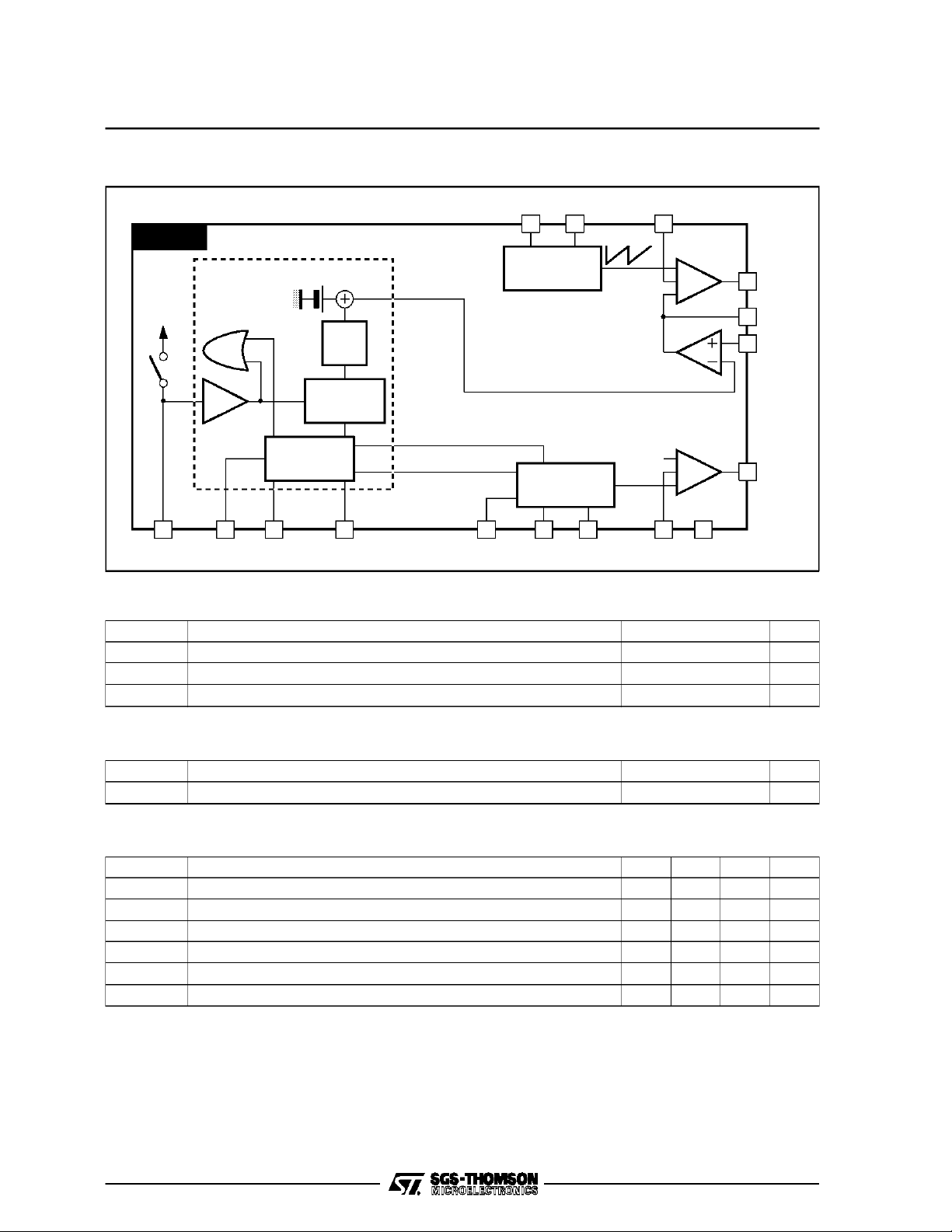
BLOCK DIAGRAM
STV5180
Internal
Supply
V
REF
D/A
8-BIT
REGISTER
16
15
SMPS
OSCILLATOR
CsfsRTsCTs
1
PWM
Error Amp
14
13
3
Pouts
Eout
E-
2
I BUS
INTERFACE
Trigger Slope Selection
Deflection ON/OFF
DEFLECTION
V Aux
PWM
5
Poutd
OSCILLATOR
2
V
STBY SDA SCL H-DRIVE CTd RTd Cfsd GND
CC
1112
4
678910
ABSOLUTEMAXIMUM RATINGS
Symbol Parameter Value Unit
V
CC
T
T
stg
SupplyVoltage 6 V
Operating Junction Temperature 150
j
Storage Temperature Range 0, + 70
THERMALDATA
Symbol Parameter Value Unit
R
th (j-a)
Junction-ambient Thermal Resistance 75
RECOMMANDED OPERATING CONDITIONS
Symbol Parameter Min. Typ. Max. Unit
V
CC
RT Timing Resistor 82
CT Timing Capacitor 1 nF
Fosc Oscillator Frequency 16 kHz
T
amb
I
SOURCE
Power Supply Voltage 4.5 5 V
Operating Ambient Temperature 0 70
Output Current (Pin 3 and Pin 5) V
= 2.5V 30 70 mA
OUT
°C
°C
°C/W
kΩ
°C
5180-02.EPS
5180-01.TBL
5180-02.TBL
5180-03.TBL
2/5
Page 3

STV5180
ELECTRICALCHARACTERISTICS(TA=25oC, VCC=5V)
Symbol Parameter Test Conditions Min. Typ. Max. Unit
SMPS OSCILLATOR
Free Period
Minimum Duty Cycle
Maximum Duty Cycle
Positive Triggering Window
Negative Triggering Window
T
ONmin
D
ONmax
W
W
T
1
SPOS
SNEG
DEFLECTION OSCILLATOR
W
W
T
D
T
OFF
DPOS
DNEG
2
ON
Free Period
Duty Cycle
Positive Triggering Window
Negative Triggering Window
INTERNAL VOLTAGE REFERENCE
V
REFmin
V
REFmax
Minimum Voltage Reference DAC set to 00 Hex 1.76 1.84 1.92 V
Maximum Voltage Reference DAC set to 3F Hex 2.08 2.16 2.24 V
POWER OUTPUT STAGES
V
POUTH
V
POUTL
I
SINK
I
SOURCE
Output High Level(Pin 3 and 5) I
Output Low Level (Pin 3 and 5) I
Sink Current (Pin3 and 5) V
Source Current(Pin 3 and 5) V
RT = 82kΩ ; CT = 1nF
RT = 82kΩ ; CT = 1nF
RT = 82kΩ ; CT = 1nF
− T
T
trig+
0
T
0
T
− T
0
T
0
RT = 82kΩ ; CT = 1nF
trig−
RT = 82kΩ ; CT = 1nF
RT = 82kΩ ; CT = 1nF
RT = 82kΩ ; CT = 1nF
RT = 82kΩ ; CT = 1nF
T
− T
trig+
0
T
0
− T
T
0
T
0
RT = 82kΩ ; CT = 1nF 20 %
trig−
RT = 82kΩ ; CT = 1nF
= 1mA 4 4.5 V
load
= -1mA 0.5 1 V
load
= 2.5V 30 70 mA
POUT
= 2.5V 30 70 mA
POUT
57 60 63.5
1.8 2.4 3
70 75 80 %
33 %
20 %
57 60 63.5
50 %
30
0%
µS
µS
µS
µS
5180-04.TBL
DAC
6 bitsDAC ; power on defaultvalue : 00 Hex.
3/5
Page 4

STV5180
SOFTWARE SPECIFICATION
2
C BusAddress
I
8C Hex.
Overview
The dataconsists of two bytes with the followingpossible values :
Byte n° Bit n° Function
1 d0to d5 DAC value for outputvoltage adjustment ; d0 = LSB ; Default= 00
d6 to d7 Subaddress 0 ; d6 = d7 = 0
2 d0 Mode switching ; Stand-by = 0 ; ON= 1 ; Default = 1
d1 H-Deflection ON/OFF ; OFF = 0 ; ON = 1 ; Default = 1
d2 Polarity H-Drive ; Chroma4 = 1 ; Philips = 0 ; Default = 0
d3 to d5 Unused
d6 to d7 Subaddress 1 ; d6 = 1 ; d7 = 0
CommandCodes
1 Normal Operating : 43 Hex
2 Stand-by : 40Hex
3 Power Stand-by : 41 Hex
4 Triggering Slope Positive : 43 Hex
5 Triggering Slope Negative : 47 Hex
6 Output VoltageAdjustment : 00 to3FHex
4/5
Page 5

PACKAGE MECHANICAL DATA
16 PINS- PLASTIC MICROPACKAGE
STV5180
GL
c1
C
A
a2
Dimensions
b
e3
D
16 9
18
Millimeters Inches
Min. Typ. Max. Min. Typ. Max.
e
M
s
F
a1
E
b1
A 1.75 0.069
a1 0.1 0.2 0.004 0.008
a2 1.6 0.063
b 0.35 0.46 0.014 0.018
b1 0.19 0.25 0.007 0.010
C 0.5 0.020
c1 45
o
(typ.)
D 9.8 10 0.386 0.394
E 5.8 6.2 0.228 0.244
e 1.27 0.050
e3 8.89 0.350
F 3.8 4.0 0.150 0.157
G 4.6 5.3 0.181 0.209
L 0.5 1.27 0.020 0.050
M 0.62 0.024
S8
o
(max.)
PM-SO16N.EPS
SO16N.TBL
Information furnished is believed to be accurate andreliable. However, SGS-THOMSON Microelectronicsassumes no responsibility
for the consequencesof useof such informationnor for any infringementof patents or other rights of thirdparties whichmay result
from its use.No licence is granted byimplication or otherwiseunder any patent or patent rightsof SGS-THOMSON Microelectronics.
Specifications mentioned in this publication are subject to change without notice. This publication supersedes and replaces all
informationpreviously supplied. SGS-THOMSON Microelectronics productsare notauthorized for useas criticalcomponents in life
support devices or systems without express written approvalof SGS-THOMSONMicroelectronics.
1994 SGS-THOMSON Microelectronics- AllRights Reserved
Purchase of I
2
I
C Patent. Rights to use these components ina I2C system, is granted provided that the system conforms to
Australia - Brazil- China - France- Germany - Hong Kong - Italy- Japan - Korea - Malaysia- Malta - Morocco
The Netherlands - Singapore - Spain - Sweden - Switzerland- Taiwan - Thailand - United Kingdom - U.S.A.
2
C Components of SGS-THOMSON Microelectronics,conveys a license under the Philips
2
the I
C Standard Specifications as defined by Philips.
SGS-THOMSON MicroelectronicsGROUP OF COMPANIES
5/5
 Loading...