

Page 1
STU16NC50
N-CHANNEL 500V - 0.22Ω - 16A Max220
PowerMesh™II MOSFET
TYPE V
DSS
R
DS(on)
I
D
STU16NC50 500V < 0.27Ω 16 A
■ TYPICAL R
■ EXTREMELY HIGH dv /d t CAPABILITY
■ 100% AVALANCHE TESTED
■ NEW HIGH VOLTAGE BENCHMARK
■ GATE CHARGE MINIMIZED
(on) = 0.22Ω
DS
DESCRIPTION
The PowerMESH
generation of MESH OVERLAY
™II is the evolution of the first
™. The layout re-
finements introduced greatly improve the Ron*area
figure of merit while keeping the device at the lea ding edge for what concerns swithing speed, gate
charge and ruggedness.
APPLICATIONS
■ HIGH CURRENT, HIGH SPEED SWITCHING
■ UNINTERRUPTIBLE POWER SUPPLIES (UPS)
■ DC-AC CONVERTERS FOR TELECOM,
INDUSTRIAL, AND LIGHTING EQUIPMENT
3
2
1
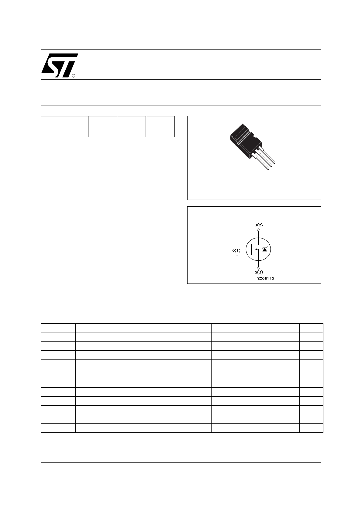
Max220
INTERNAL SCHEMATIC DIAGRAM
ABSOLUTE MAXIMUM RATINGS
Symbol Parameter Value Unit
V
DS
V
DGR
V
GS
I
D
I
D
I
DM
P
TOT
dv/dt(1) Peak Diode Recovery voltage slope 3 V/ns
T
stg
T
j
(•)Pu l se width limite d by safe operat i ng area
Drain-source Voltage (VGS = 0)
Drain-gate Voltage (RGS = 20 kΩ)
500 V
500 V
Gate- source Voltage ±30 V
Drain Current (continuos) at TC = 25°C
Drain Current (continuos) at TC = 100°C
(●)
Drain Current (pulsed) 64 A
Total Dissipation at TC = 25°C
16 A
10 A
160 W
Derating Factor 1.28 W/°C
Storage Temperature –65 to 150 °C
Max. Operating Junction Temperature 150 °C
(1)ISD ≤16A, di/dt ≤100A/µs, VDD ≤ V
(BR)DSS
, Tj ≤ T
JMAX.
1/8October 2001
Page 2
STU16NC50
THERMA L D ATA
Rthj-case Thermal Resistance Junction-case Max 0.78 °C/W
Rthj-amb Thermal Resistance Junction-ambient Max 62.5 °C/W
T
l
AVALANCHE CHARACTERISTICS
Symbol Parameter Max Value Unit
I
AR
E
AS
ELECTRICAL CHARACTERISTICS (TCASE = 25 °C UNLESS OTHERWISE SPECIFIED)
OFF
Symbol Parameter Test Conditions Min. Typ. Max. Unit
V
(BR)DSS
I
DSS
I
GSS
Maximum Lead Temperature For Soldering Purpose 300 °C
Avalanche Current, Repetitive or Not-Repetitive
(pulse width limited by T
max)
j
Single Pulse Avalanche Energy
(starting T
Drain-source
= 25 °C, ID = IAR, VDD = 50 V)
j
ID = 250 µA, VGS = 0 500 V
16 A
1000 mJ
Breakdown Voltage
Zero Gate Voltage
Drain Current (V
GS
Gate-body Leakage
Current (V
DS
= 0)
= 0)
V
= Max Rating
DS
V
= Max Rating, TC = 125 °C
DS
V
= ±30V ±100 nA
GS
1µA
50 µA
(1)
ON
Symbol Parameter Test Conditions Min. Typ. Max. Unit
V
GS(th)
R
DS(on)
Gate Threshold Voltage
Static Drain-source On
V
= VGS, ID = 250 µA
DS
VGS = 10V, ID = 9A
234V
0.22 0.27 Ω
Resistance
DYNAMIC
Symbol Parameter Test Conditions Min. Typ. Max. Unit
g
fs
C
iss
C
oss
C
rss
Forward Transconductance VDS > I
I
=9A
D
Input Capacitance
V
DS
Output Capacitance 410 pF
Reverse Transfer
Capacitance
D(on)
x R
DS(on)max,
= 25V, f = 1 MHz, VGS = 0
18 S
2980 pF
58 pF
2/8
Page 3
STU16NC50
ELECTRICAL CHARACTERISTICS (CONTINUED)
SWITCHING ON
Symbol Parameter Test Conditions Min. Typ. Max. Unit
t
d(on)
t
Q
Q
Q
gd
r
g
gs
Turn-on Delay Time
Rise Time
Total Gate Charge
Gate-Source Charge 14.7 nC
Gate-Drain Charge 41.7 nC
SWITCHING OFF
Symbol Param eter Test Conditions Min. Typ. Max. Unit
t
r(Voff)
t
t
f
c
Off-voltage Rise Time
Fall Time 30 ns
Cross-over Time 58 ns
SOURCE DRAIN DIODE
Symbol Parameter Test Conditions Min. Typ. Max. Unit
I
SD
I
SDM
V
SD
t
rr
Q
rr
I
RRM
Note: 1. Pulsed: Pul se duration = 300 µs, duty cycle 1.5 %.
2. Pulse width l i m i t ed by safe operat i ng area.
Source-drain Current 16 A
(2)
Source-drain Current (pulsed) 64 A
(1)
Forward On Voltage
Reverse Recovery Time
Reverse Recovery Charg e 5 µ C
Reverse Recovery Curren t 21 A
= 250V, ID = 10 A
V
DD
RG= 4.7Ω VGS = 10V
(see test circuit, Figure 3)
V
= 400V, ID = 20 A,
DD
VGS = 10V
VDD = 400V, ID = 20 A,
RG= 4.7Ω, V
GS
= 10V
(see test circuit, Figure 5)
I
= 18.4 A, VGS = 0
SD
= 20 A, di/dt = 100A/µs,
I
SD
V
= 100V, Tj = 150°C
DD
(see test circuit, Figure 5)
29 ns
21 ns
95 128 nC
14 ns
1.6 V
480 ns
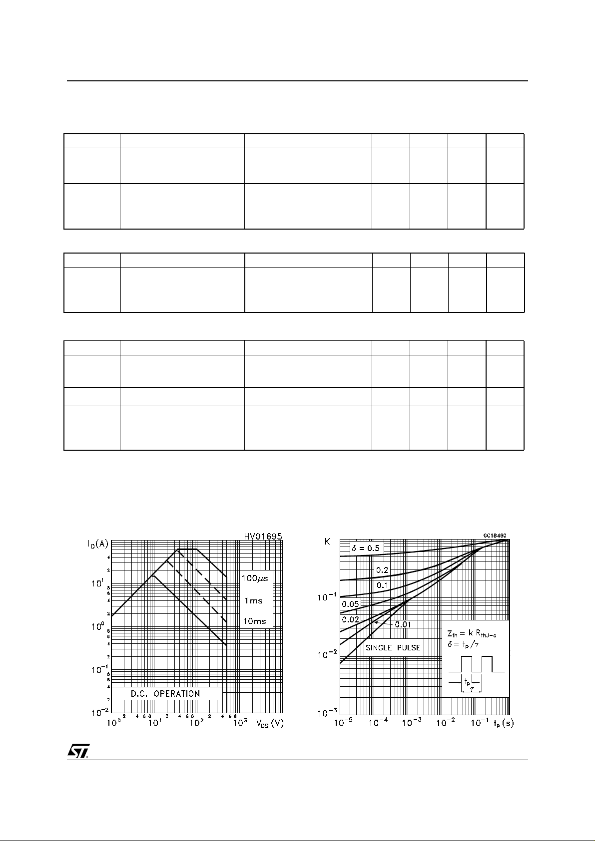
Safe Operating Area Thermal Impedance
3/8
Page 4

STU16NC50
Output Characteristics Transfer Characteristics
Transconductance
Gate Charge vs Gate-source Voltage
Static Drain-source On Resistance
Capacitance Variations
4/8
Page 5

STU16NC50
Normalized Gate Thereshold Voltage vs Temp. Normalized On Resistance vs Temp eratur e
Source-drain Diode Forward Characteristics
5/8
Page 6

STU16NC50
Fig. 2: Unclamped Inductive WaveformFig. 1: Unclamped Inductive Load Test Circuit
Fig. 3: Switching Times Test Circuit For
Resistive Load
Fig. 5: Test Circuit For Inductive Load Switching
And Diode Recovery Times
Fig. 4: Gate Charge test Circuit
6/8
Page 7

Max220 MECHANICAL DATA
STU16NC50
DIM.
MIN. TYP. MAX. MIN. TYP. MAX.
A 4.3 4.6 0.169 0.181
A1 2.2 2.4 0.087 0.094
A2 2.9 3.1 0.114 0.122
b 0.7 0.93 0.027 0.036
b1 1.25 1.4 0.049 0.055
b2 1.2 1.38 0.047 0.054
c 0.45 0.6 0.18 0.023
D 15.9 16.3 0.626 0.641
D1 9 9.35 0.354 0.368
D2 0.8 1.2 0.031 0.047
D3 2.8 3.2 0.110 0.126
e 2.44 2.64 0.096 0.104
E 10.05 10.35 0.396 0.407
L 13.2 13.6 0.520 0.535
L1 3 3.4 0.118 0.133
D3 D1
A
mm inch
D2
A2
C
A1
D
b1
b2
E
L1
L
b
e
P011R
7/8
Page 8

STU16NC50
Information furnishe d is bel i eved to be accurate and reliable. However, STMicroelectro ni cs assumes no responsibility for t he co nsequen ces
of use of such information nor for any infringement of patents or other rights of third parties which may result from its use. No license is granted
by implic ation or oth erwise unde r any patent or patent rights of ST M i croelectronics. Specification s mentioned in this pub l ic at i on are s ubject
to change without notice. This publication supersedes and replaces all information previously supplied. STMicroelectronics products are not
authorized for use as critical components in life su pport devices or systems wit hout express wri tten approv al of STMicroelectronics.
The ST log o i s registered tr ademark of STMi croelect ronics
2000 STMicroelectronics - All Rights Rese rved
All other names are the property of the i r respective owners.
Australi a - B razil - China - Finland - France - Germany - Hong Kong - India - Italy - Japan - Malaysi a - M al ta - Morocc o -
Singapor e - Spain - Swede n - S wi tzerland - U ni ted Kingdom - U.S.A.
STMicroelectron ics GROUP OF COMPANIES
http://www.st.com
8/8
 Loading...