

Page 1
LOW DROPPOWER SCHOTTKY RECTIFIER
MAINPRODUCTSCHARACTERISTICS
STPS30L40CG/CT/CW
I
F(AV)
V
RRM
2 x 15A
40 V
Tj (max) 150 °C
V
(max) 0.50 V
F
FEATURESAND BENEFITS
VERYSMALLCONDUCTION LOSSES
NEGLIGIBLESWITCHINGLOSSES
LOWFORWARD VOLTAGEDROP
LOWTHERMALRESISTANCE
AVALANCHERATED
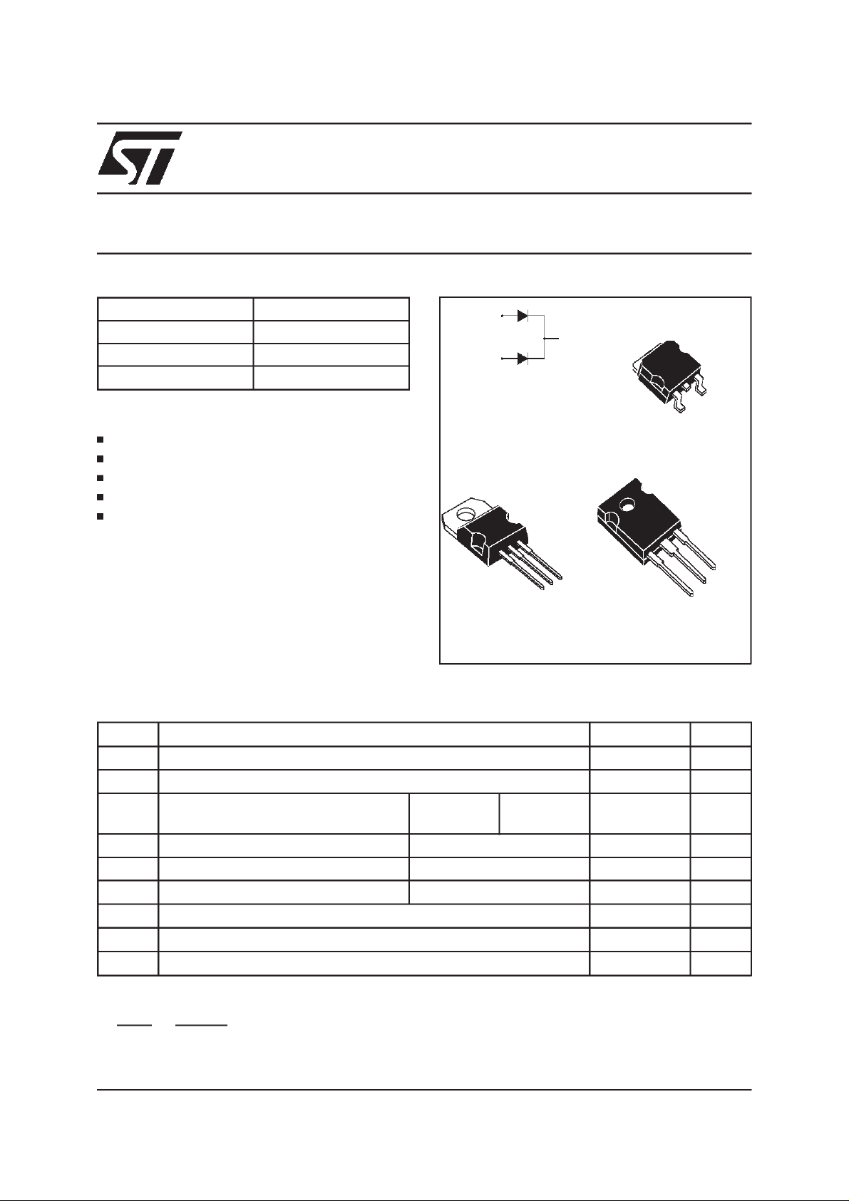
DESCRIPTION
Dual center tap schottky rectifiers suited for
Switched Mode Power Supplies and high
frequencyDC to DCconverters.
2
PackagedinTO-247,TO-220ABandD
PAKthese
devicesare intended for use in low voltage,high
frequency inverters, free-wheeling and polarity
protectionapplications.
ABSOLUTE RATINGS
(limitingvalues,per diode)
A1
A2
A1
TO-220AB
STPS30L40CT
K
K
A2
A1
2
PAK
D
STPS30L40CG
A2
K
A2
K
A1
TO-247
STPS30L40CW
Symbol Parameter Value Unit
V
RRM
I
F(RMS)
I
F(AV)
I
FSM
I
RRM
I
RSM
T
stg
Tj
dV/dt
dPtot
*:
dTj
July 1999 -Ed: 3A
Repetitivepeak reverse voltage
RMSforwardcurrent
Averageforward current Tc= 135°C
Surgenonrepetitiveforwardcurrent tp = 10 ms Sinusoidal
Repetitivepeak reverse current tp=2µs square F=1kHz
Non repetitivepeakreverse current tp = 100 µs square
Storagetemperaturerange
Maximumoperatingjunction temperature*
Criticalrateof riseofreversevoltage
<
Rth(j
δ =0.5
1
thermal runawayconditionfor a diode on its own heatsink
a
)
−
Per diode
Per device
40 V
30 A
15
30
220 A
1A
3A
- 65 to+ 150 °C
150 °C
10000 V/µs
A
1/6
Page 2
STPS30L40CG/CT/CW
THERMAL RESISTANCES
Symbol Parameter Value Unit
R
th (j-c)
R
th (c)
Junctionto case
Whenthediodes1 and2 areused simultaneously:
∆ Tj(diode1)= P(diode1)x R
(Perdiode) + P(diode2)x R
th(j-c)
Per diode
Total
Coupling 0.10 °C/W
th(c)
1.60
0.85
°C/W
STATICELECTRICALCHARACTERISTICS
(per diode)
Symbol Parameter TestsConditions Min. Typ. Max. Unit
*
I
R
V
F
Reverseleakage
current
*
Forward voltagedrop Tj =25°CI
Tj = 25°CV
Tj = 100°C
Tj = 125°CI
Tj = 25°CI
Tj = 125°CI
R=VRRM
=15A
F
=15A
F
=30A
F
=30A
F
20 50 mA
0.42 0.50
0.59 0.67
360 µA
0.55 V
0.74
Pulsetest: * tp = 380µs,δ<2%
Toevaluatethe conductionlossesusethe followingequation:
P = 0.330 x I
F(AV)
+0.011I
F2(RMS)
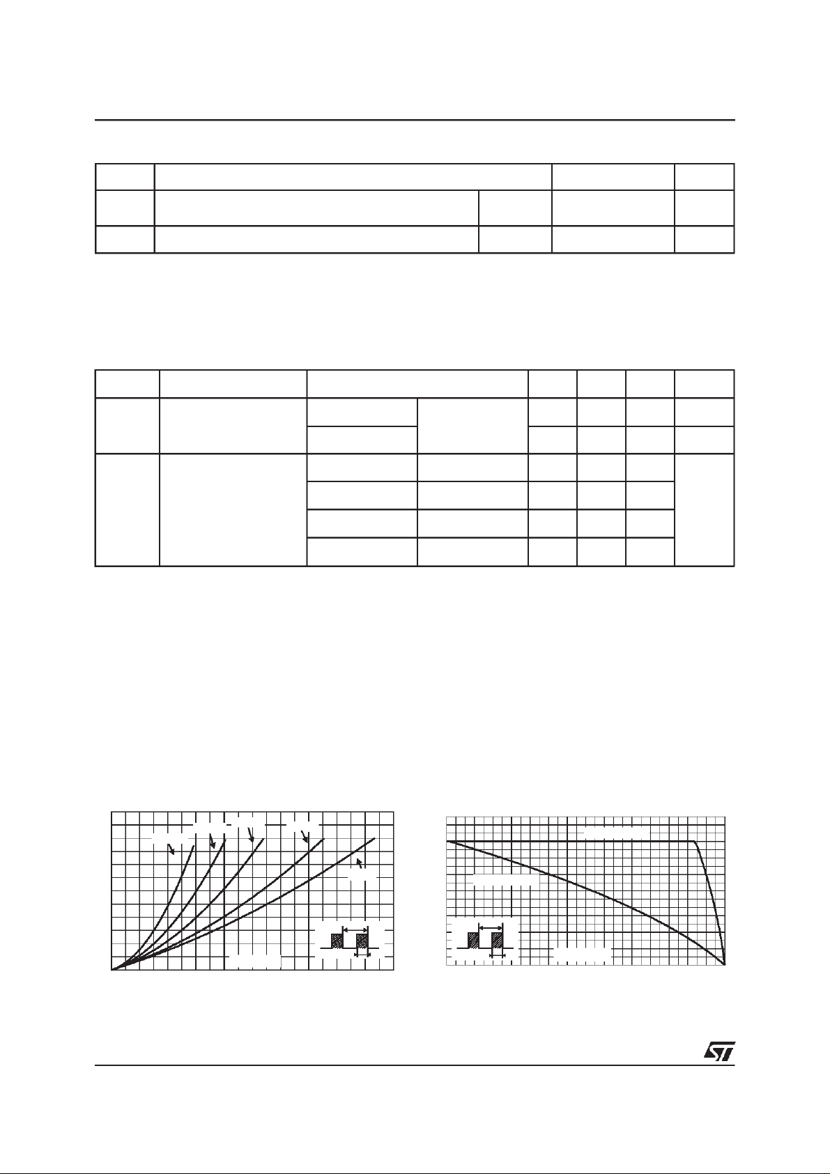
Fig. 1: Average forward power dissipation versus
averageforwardcurrent(per diode).
PF(av)(W)
12
10
8
6
4
2
0
02468101214161820
2/6
δ = 0.05
δ = 0.1
δ = 0.2
IF(av)A
δ= 0.5
δ =1
T
=tp/T tp
δ
Fig. 2:
Average current versus ambient
temperature(δ=0.5) (perdiode).
IF(av)(A)
18
16
14
12
10
Rth(j-a)=15°C/W
8
6
4
2
0
0 25 50 75 100 125 150
δ
=tp/T
T
tp
Rth(j-a)=Rth(j-c)
Tamb(°C)
Page 3

STPS30L40CG/CT/CW
Fig. 3: Non repetitive surge peak forward current
versus overload duration (maximum values) (per
diode).
IM(A)
200
180
160
140
120
100
80
60
IM
40
20
0
1E-3 1E-2 1E-1 1E+0
δ=0.5
t
t(s)
Tc=25°C
Tc=75°C
Tc=125°C
Fig. 5: Reverse leakage current versus reverse
voltageapplied (typicalvalues)(perdiode).
IR(mA)
2E+2
1E+2
1E+1
1E+0
Tj=150°C
Tj=100°C
Tj=75°C
Fig. 4: Relative variation of thermal transient
impedancejunctionto caseversuspulseduration.
Zth(j-c)/Rth(j-c)
1.0
0.8
δ = 0.5
0.6
0.4
δ = 0.2
δ = 0.1
0.2
0.0
1.0E-4 1.0E-3 1.0E-2 1.0E-1 1.0E+0
Fig. 6:
Single pulse
tp(s)
Junction capacitance versus reverse
T
=tp/T tp
δ
voltageapplied(typicalvalues)(perdiode).
C(pF)
2000
1000
500
F=1MHz
Tj=25°C
1E-1
1E-2
0 5 10 15 20 25 30 35 40
Fig. 7:
Forward voltage drop versus forward
Tj=25°C
VR(V)
current(maximumvalues)(per diode).
IFM(A)
200
100
10
1
0.0 0.2 0.4 0.6 0.8 1.0 1.2 1.4 1.6 1.8 2.0
Typicalvalues
Tj=150°C
Tj=125°C
Tj=25°C
VFM(V)
200
100
12 51020 50
Fig. 8 :
Thermal resistance junction to ambient
VR(V)
versus copper surface under tab (Epoxy printed
circuitboardFR4,copperthickness: 35µm)
(STPS30L40CGonly).
Rth(j-a) (°C/W)
80
70
60
50
40
30
20
10
0
0 5 10 15 20 25 30 35 40
S(Cu) (cm )
3/6
Page 4

STPS30L40CG/CT/CW
PACKAGEMECHANICALDATA
TO-220AB
H2
Dia
L5
L6
L2
F2
F1
F
G1
G
L9
L4
DIMENSIONS
REF.
A
C
A 4.40 4.60 0.173 0.181
C 1.23 1.32 0.048 0.051
Millimeters Inches
Min. Max. Min. Max.
D 2.40 2.72 0.094 0.107
L7
E 0.49 0.70 0.019 0.027
F 0.61 0.88 0.024 0.034
F1 1.14 1.70 0.044 0.066
F2 1.14 1.70 0.044 0.066
G 4.95 5.15 0.194 0.202
D
G1 2.40 2.70 0.094 0.106
H2 10 10.40 0.393 0.409
L2 16.4typ. 0.645typ.
L4 13 14 0.511 0.551
L5 2.65 2.95 0.104 0.116
M
E
L6 15.25 15.75 0.600 0.620
L7 6.20 6.60 0.244 0.259
L9 3.50 3.93 0.137 0.154
M 2.6typ. 0.102 typ.
Diam. 3.75 3.85 0.147 0.151
Coolingmethod: C
Recommendedtorque value: 0.55m.N
Maximumtorque value : 0.70m.N
4/6
Page 5

PACKAGEMECHANICAL DATA
2
PAK
D
L2
L
L3
E
A1
B2
B
G
C2
STPS30L40CG/CT/CW
DIMENSIONS
REF.
A
A 4.40 4.60 0.173 0.181
A1 2.49 2.69 0.098 0.106
A2 0.03 0.23 0.001 0.009
D
B 0.70 0.93 0.027 0.037
B2 1.14 1.70 0.045 0.067
C 0.45 0.60 0.017 0.024
C2 1.23 1.36 0.048 0.054
D 8.95 9.35 0.352 0.368
E 10.00 10.40 0.393 0.409
C
R
G 4.88 5.28 0.192 0.208
L 15.00 15.85 0.590 0.624
L2 1.27 1.40 0.050 0.055
L3 1.40 1.75 0.055 0.069
A2
M 2.40 3.20 0.094 0.126
R 0.40typ. 0.016 typ.
V2 0° 8° 0° 8°
M
*
V2
Millimeters Inches
Min. Max. Min. Max.
* FLATZONE NO LESSTHAN 2mm
Coolingmethod: byconduction(method C)
FOOT PRINT (in millimeters)
2
PAK
D
16.90
10.30
1.30
8.90
3.70
5.08
5/6
Page 6

STPS30L40CG/CT/CW
PACKAGEMECHANICAL DATA
TO-247
V
V
H
L5
L
F2
F4
L1
F3
L3
F1
V2
F(x3)
G
==
Dia.
L4L2
ME
A
D
DIMENSIONS
REF.
Millimeters Inches
Min. Typ. Max. Min. Typ. Max.
A 4.85 5.15 0.191 0.203
D 2.20 2.60 0.086 0.102
E 0.40 0.80 0.015 0.031
F 1.00 1.40 0.039 0.055
F1 3.00 0.118
F2 2.00 0.078
F3 2.00 2.40 0.078 0.094
F4 3.00 3.40 0.118 0.133
G 10.90 0.429
H 15.45 15.75 0.608 0.620
L 19.85 20.15 0.781 0.793
L1 3.70 4.30 0.145 0.169
L2 18.50 0.728
L3 14.20 14.80 0.559 0.582
L4 34.60 1.362
L5 5.50 0.216
M 2.00 3.00 0.078 0.118
V5° 5°
V2 60° 60°
Dia. 3.55 3.65 0.139 0.143
Coolingmethod: C
Recommendedtorquevalue: 0.8m.N
Maximumtorque value : 1.0m.N
Orderingtype Marking Package Weight Baseqty Delivery mode
STPS30L40CT STPS30L40CT TO-220AB 2g 50 Tube
STPS30L40CG STPS30L40CG D
STPS30L40CG-TR STPS30L40CG D
2
PAK 1.8g 50 Tube
2
PAK 1.8g 500 Tape& reel
STPS30L40CW STPS30L40CW TO-247 4.4g 30 Tube
EpoxymeetsUL94,V0
Informationfurnished is believedto beaccurate andreliable. However, STMicroelectronics assumes noresponsibility for theconsequences of
use ofsuch informationnor forany infringementof patentsor otherrights of third parties which mayresult fromitsuse. Nolicense is granted by
implication or otherwise under any patent or patent rights of STMicroelectronics.Specifications mentioned in this publication are subject to
change without notice. This publication supersedes andreplacesall informationpreviously supplied.
STMicroelectronics products are not authorized for use as critical components in life support devices or systems without express written approval ofSTMicroelectronics.
The ST logo is a registered trademark of STMicroelectronics
1999 STMicroelectronics- Printed inItaly - All rights reserved.
STMicroelectronics GROUP OF COMPANIES
Australia -Brazil - China - Finland - France - Germany - Hong Kong- India - Italy -Japan - Malaysia
Malta - Morocco - Singapore - Spain - Sweden - Switzerland - United Kingdom -U.S.A.
http://www.st.com
6/6
 Loading...