

Page 1
®
MAIN PRODUCT CHARACTERISTICS
STPS3045G
POWER SCHO TTKY REC TIFIER
Tj
V
I
F(AV)
V
RRM
(max)
(max)
F
30 A
45 V
175°C
0.63 V
K
FEATURES AND BE NE F ITS
VERY SMALL CONDUCTION LOSS ES
NEGLIGIBLE SWIT CHING LOS SE S
EXTRE MELY F AST SWI TCHI NG
A
A
LOW THERMAL RESISTANCE
HIGH DISSIPATION M INIATURE PACKAGE
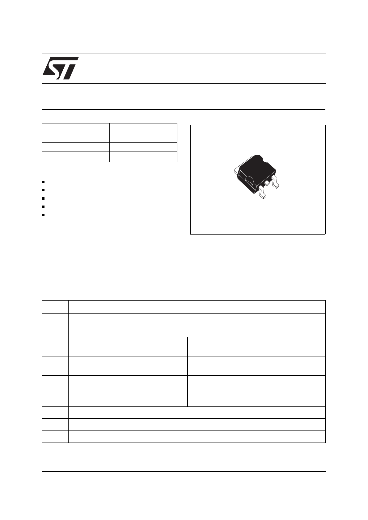
D
2
PAK
DESCRIPTION
Single Schottky rectifier suited for switchmode
power supply and high frequency DC to DC converters.
2
Packaged in D
PAK surface mount package , this
device is intended for use in low voltage, high frequency inverters, free wheeling and polarity pr otection applications.
ABSOLUTE RATINGS
(limiting values)
Symbol Parameter Value Unit
V
RRM
I
F(RMS)
I
F(AV)
I
FSM
Repetitive peak reverse voltage 45 V
RMS forward current 50 A
Average forward current Tc = 150°C
δ
= 0.5
Surge non repetitive forward current tp = 10 ms
30 A
200 A
Sinusoidal
I
RRM
Repetitive peak reverse current tp = 2 µs
1A
F = 1kHz square
I
RSM
Non Repetitive peak reverse current tp = 100µs square 3 A
Tstg Storage temperature range - 65 to + 175
Tj Maximum operating junction temperature* 175 °C
dV/dt Critical rate of rise of reverse voltage 10000 V/µs
dPtot
dTj
* :
October 1999 - Ed: 4A
1
<
Rth
thermal runaway condition for a diode on its own heatsink
(
)
j−a
°
C
1/5
Page 2

STPS3045G
THERMAL RE SISTA NC ES
Symbol Parameter Value Unit
R
th (j-c)
Junction to case 1
°
STATIC ELECTRICAL CHARACTER ISTICS
Symbol Parameter Tests Conditions Min. Typ. Max. Unit
* Reverse leakage current Tj = 25°CV
I
R
= V
R
RRM
500
Tj = 125°C2080mA
** Forward voltage drop Tj = 125°CI
V
F
Tj = 25°CI
Tj = 125°CI
Pulse test : * tp = 5 ms, δ < 2 %
** tp = 380 µs, δ < 2%
= 30 A 0.53 0.63 V
F
= 60 A 0.84
F
= 60 A 0.68 0.78
F
To evaluate the conduction losses use the following equation :
P = 0.48 x I
F(AV)
+ 0.005 I
F2(RMS)
C/W
µ
A
Fig. 1:
Average forward power dissipation versus
average forward current.
PF(av)(W)
25
20
15
10
5
0
0 5 10 15 20 25 30 35 40
δ = 0.05
δ = 0.1
δ = 0.2
IF(av) (A)
δ = 0.5
δ
δ = 1
T
=tp/T
Fig. 2:
Average forward current versus ambient
temperature (δ=0.5).
IF(av)(A)
35
30
25
20
15
Rth(j-a)=30°C/W
10
tp
5
0
0 25 50 75 100 125 150 175
Rth(j-a)=Rth(j-c)
Tamb(°C)
δ
=tp/T
T
tp
2/5
Page 3

Fig. 3:
Non repetitive surge peak forward current
versus overload duration (maximum values).
STPS3045G
Fig. 4:
junction to case versus pulse duration.
Relative variation of thermal impedance
IM(A)
400
350
300
250
200
150
100
I
M
50
0
1E-3 1E-2 1E-1 1E+0
Fig. 5:
t
δ
=0.5
t(s)
Reverse leakage current versus reverse
Tc=75°C
Tc=100°C
Tc=125°C
voltage applied (typical values)
IR(µA)
1E+5
1E+4
1E+3
Tj=150°C
Tj=125°C
Tj=100°C
Tj=75°C
Zth(j-c)/Rth(j-c)
1.0
0.8
δ = 0.5
0.6
0.4
δ = 0.2
δ = 0.1
0.2
Single pulse
0.0
1E-4 1E-3 1E-2 1E-1 1E+0
Fig. 6:
Junction capacitance versus reverse
tp(s)
δ
=tp/T
T
tp
voltage applied (typical values).
C(nF)
5.0
1.0
F=1MHz
Tj=25°C
1E+2
1E+1
Tj=50°C
Tj=25°C
VR(V)
1E+0
0 5 10 15 20 25 30 35 40 45
Fig. 7:
Forward voltage drop versus forward current
(maximum values).
IFM(A)
200
100
10
1
0.0 0.2 0.4 0.6 0.8 1.0 1.2 1.4
Typical values
Tj=125°C
Tj=25°C
Tj=125°C
VFM(V)
0.1
12 51020 50
Fig. 8:
Thermal resistance junction to ambient versus copper surface under tab (Epoxy printed c ircuit
board, copper thickness: 35µm)
Rth(j-a) (°C/W)
80
70
60
50
40
30
20
VR(V)
10
0
0 2 4 6 8 101214161820
S(Cu) (cm²)
3/5
Page 4

STPS3045G
PACKAGE MECHANICAL DAT A
2
D
PAK
E
L2
L
L3
A1
B2
B
G
* FLAT ZONE NO LESS THAN 2mm
C2
DIMENSIONS
REF.
A
Millimeters Inches
Min. Max. Min. Max.
A 4.40 4.60 0.173 0.181
A1 2.49 2.69 0.098 0.106
A2 0.03 0.23 0.001 0.009
D
B 0.70 0.93 0.027 0.037
B2 1.14 1.70 0.045 0.067
C 0.45 0.60 0.017 0.024
C2 1.23 1.36 0.048 0.054
C
R
D 8.95 9.35 0.352 0.368
E 10.00 10.40 0.393 0.409
G 4.88 5.28 0.192 0.208
A2
L 15.00 15.85 0.590 0.624
L2 1.27 1.40 0.050 0.055
L3 1.40 1.75 0.055 0.069
M
*
V2
M 2.40 3.20 0.094 0.126
R 0.40 typ. 0.016 typ.
V2 0° 8° 0° 8°
FOOTPRINT DIMENSIONS
16.90
10.30
8.90
(in millimeters)
5.08
1.30
3.70
4/5
Page 5

STPS3045G
Type Marking Package Weight Base qty Delivery mode
2
STPS3045G ST PS3045G D
STPS3045G-TR STPS3045G D
Epoxy meets UL94, V0
PAK 1.48g 50 Tube
2
PAK 1.48g 500 Tape & Reel
Information furnished is believed to be accurate and reliable. However, STMicroelectronics assumes no responsibility for the consequences of
use of such information nor for any infringement of patents or other rights of third parties which may result from its use. No license is granted by
implication or otherwi se un der any pat ent or patent rights of STMic roelec tronics. S pecifications ment ioned in t his publ ication are subject to
change without notice. This publication supersedes and replaces all information previously supplied.
STMicroelectronics products are not authorized for use as crit ic al components in life support devices or systems wi thout express writte n approval of STMicroelectronics.
The ST logo is a registered trademark of STMicroe lectronics
© 1999 STMicroelectronics - Printed in Italy - All rights reser ved.
STMicroelectronics GROUP OF COMPANIES
Australia - Brazil - China - Finland - France - Germany - Hong Kong - India - Italy - Japan - Malaysia
Malta - Morocco - Singapore - Spain - Sweden - Switzerland - United Kingdom - U.S.A.
http://www.st.com
5/5
 Loading...