

Page 1
STPS2545C
Power Schottky rectifier
Datasheet − production data
Features
■ Very small conduction losses
■ Negligible switching losses
■ Extremely fast switching
■ Low thermal resistance
■ Avalanche capability specified
■ ECOPACK
®
2 compliant component
(STPS2545CT)
Description
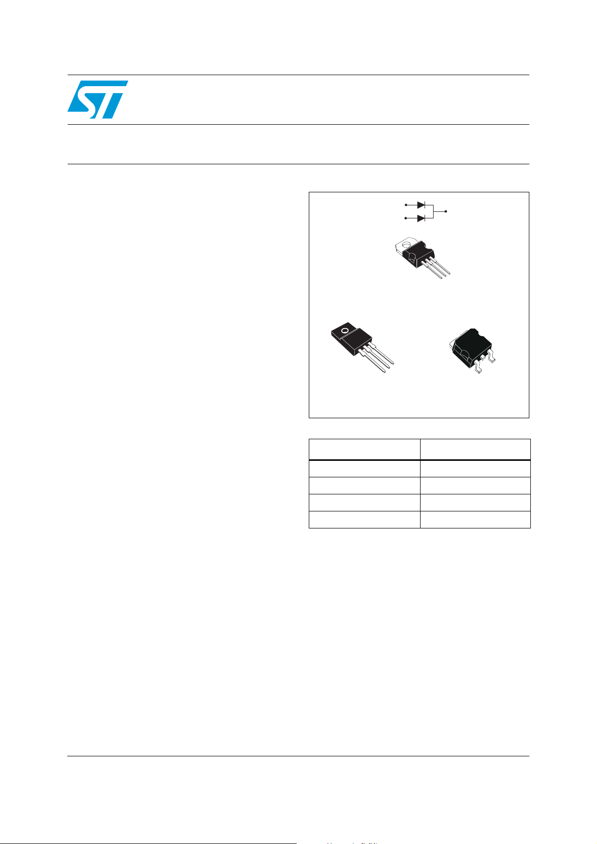
Dual center tab Schottky rectifier suited for switch
mode power supplies and high frequency DC to
DC converters.
This device is especially intended for use in low
volage, high frequency inverters, free-wheeling
and polarity protection applications.
A1
A2
TO-220AB
STPS2545CT
A2
K
A1
TO-220FPAB
STPS2545CFP
Table 1. Device summary
Symbol Value
I
2 x 12.5 A
F(AV)
45 V
V
RRM
T
j (max)
V
0.57 V
F(max)
K
A2
K
A1
K
A1
2
PAK
D
STPS2545CG
175 °C
A2
June 2012 Doc ID 8736 Rev 4 1/10
This is information on a product in full production.
www.st.com
10
Page 2
Characteristics STPS2545C
1 Characteristics
Table 2. Absolute ratings (limiting values, per diode)
Symbol Parameter Value Unit
V
I
F(RMS)
I
F(AV)
I
I
I
P
T
Repetitive peak reverse voltage 45 V
RRM
Forward rms current 30 A
2
Average forward current
δ = 0.5
Surge non repetitive forward current t
FSM
Repetitive peak reverse current
RRM
Non repetitive peak reverse current
RSM
Repetitive peak avalanche power
ARM
Storage temperature range -65 to + 175 °C
stg
Maximum operating junction temperature
T
j
TO-220AB D
TO-220FPAB
PA K
(1)
=160 °C
T
c
T
=140 °C
c
= 10 ms sinusoidal 200 A
p
= 2 µs square F=1 kHz
t
p
= 100 µs square
t
p
= 1 µs Tj = 25 °C
t
p
Per diode 12.5
Per device 25
1 A
2A
4800 W
175 °C
A
dV/dt Critical rate of rise reverse voltage 10000 V/µs
<
Rth(j-a)
1
dPtot
1. condition to avoid thermal runaway for a diode on its own heatsink
dTj
Table 3. Thermal resistances
Symbol Parameter Value Unit
2
TO-220AB / D
PAK Per diode 1.6
° C/W
TO-220FPAB 4
Junction to case
R
th (j-c)
TO-220AB / D2PAK Total 1.1
° C/W
TO-220FPAB 3.5
2
PA K 0 .6
° C/W
R
th (c)
Coupling
TO-220AB / D
TO-220FPAB 3
When the diodes 1 and 2 are used simultaneously :
ΔTj(diode 1) = P(diode1) x R
2/10 Doc ID 8736 Rev 4
(Per diode) + P(diode 2) x R
th(j-c)
th(c)
Page 3
STPS2545C Characteristics
Table 4. Static electrical characteristics (per diode)
Symbol Parameter Tests Conditions Min. Typ. Max. Unit
(1)
I
Reverse leakage current
R
(1)
VF
Forward voltage drop
1. Pulse test : tp = 380 µs, δ < 2%
Tj = 25 °C
= 125 °C 9 25 mA
VR = V
T
j
= 125 °C IF = 12.5 A 0.50 0.57
T
j
= 25 °C IF = 25 A 0.84
j
= 125 °C IF = 25 A 0.65 0.72
T
j
RRM
125 µA
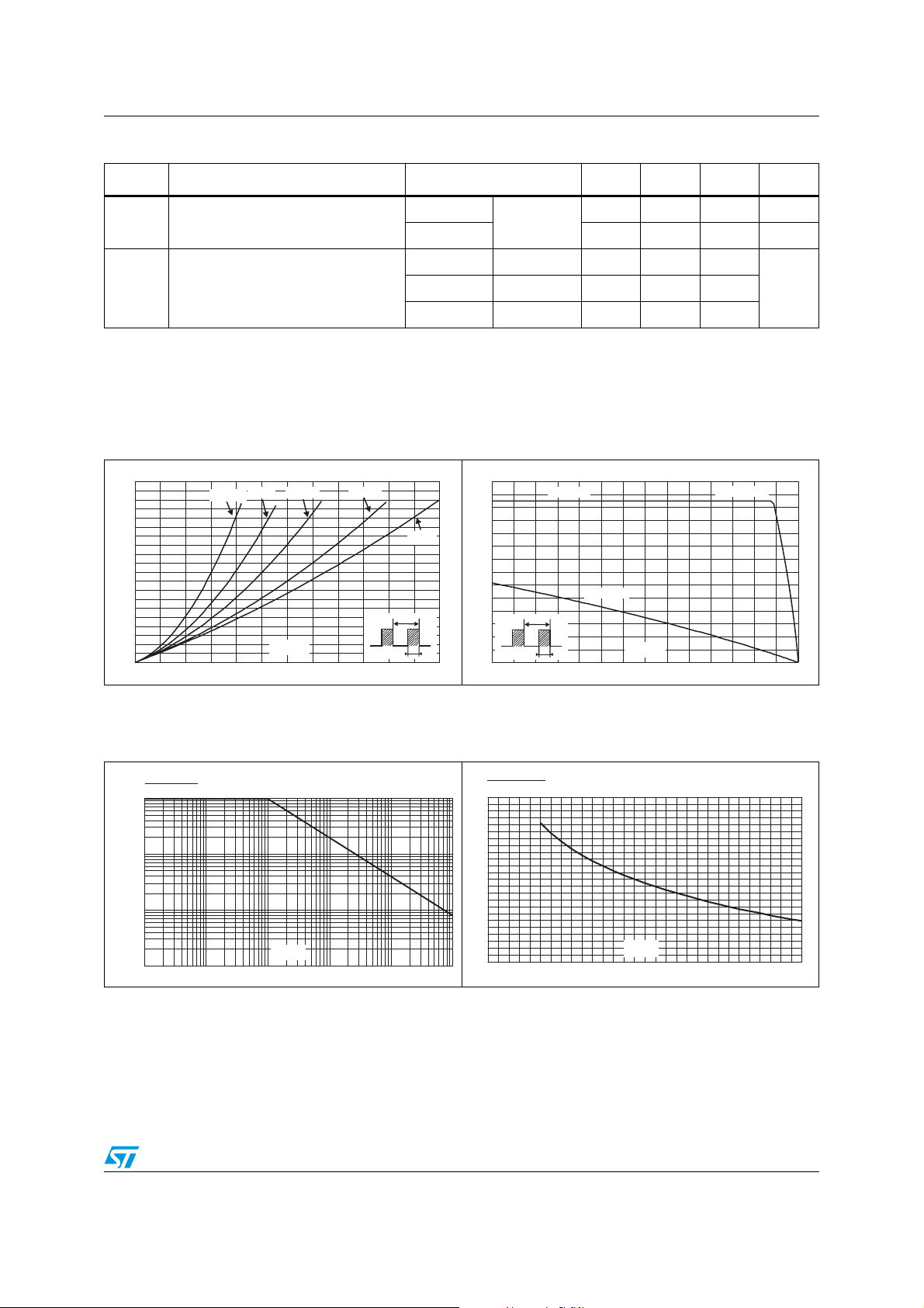
To evaluate the conduction losses use the following equation :
P = 0.42 x I
Figure 1. Conduction losses versus average
current)
P (W)F(AV)
10
9
8
7
6
5
4
3
2
1
0
0.0 2.5 5.0 7.5 10.0 12.5 15.0
δ = 0.05
δ = 0.1
Figure 3. Normalized avalanche power
derating versus pulse duration
+ 0.012 x I
F(AV)
δ = 0.2
I (A)F(AV)
δ = 0.5
F2(RMS)
T
=tp/T
δ
δ = 1
Figure 2. Average forward current versus
ambient temperature (δ = 0.5)
I (A)F(AV)
14
12
10
8
6
4
2
tp
δ
0
0 25 50 75 100 125 150 175
=tp/T
Rth
=Rth
(j-a)
(j-c)
Rth
=50°C/W
(j-a)
T
tp
T (°C)amb
Figure 4. Normalized avalanche power
derating versus junction
TO-220AB/D²PAK
temperature
P(t)
P(t)
ARM p
P (1µs)
ARM
1
P (25°C)
ARM
1.2
1
ARM p
V T
0.1
0.01
0.001
0.10.01 1
t (µs)
p
10 100 1000
0.8
0.6
0.4
0.2
T (°C)
0
j
0 25 50 75 100 125 150
Doc ID 8736 Rev 4 3/10
Page 4

Characteristics STPS2545C
Figure 5. Non repetitive surge peak forward
current versus overload duration
(maximum values)
I (A)M
200
180
160
140
120
100
80
60
40
IM
20
0
1.E-03 1.E-02 1.E-01 1.E+00
δ=0.5
t
t(s)
TO-220AB, D PAK
2
TC=25°C
TC=75°C
TC=125°C
Figure 7. Relative variation of thermal
impedance junction to case versus
pulse duration (TO-220AB, D
Zth(j-c) / Rth(j-c)
1.0
0.9
0.8
0.7
δ = 0.5
0.6
0.5
0.4
δ = 0.2
δ = 0.1
0.3
0.2
Single pulse
0.1
0.0
1.E-03 1.E-02 1.E-01 1.E+00
t (s)
P
δ
=tp/T
2
T
PAK)
tp
Figure 9. Reverse leakage current versus
reverse voltage applied
(typical values)
I (mA)R
1.E+02
1.E+01
Tj=150°C
Tj=125°C
Figure 6. Relative variation of thermal
impedance junction to case versus
pulse duration (TO-220FPAB)
I (A)M
120
100
80
60
40
IM
20
0
1.E-03 1.E-02 1.E-01 1.E+00
δ=0.5
t
t(s)
TC=25°C
TC=125°C
Figure 8. Relative variation of thermal
impedance junction to case versus
pulse duration (TO-220FPAB)
Zth(j-c) / Rth(j-c)
1.0
0.9
0.8
0.7
0.6
= 0.5
δ
0.5
0.4
= 0.2
δ
0.3
= 0.1
δ
0.2
0.1
Single pulse
0.0
1.E-03 1.E-02 1.E-01 1.E+00 1.E+01
t (s)
P
δ
T
=tp/T
Figure 10. Junction capacitance versus
reverse voltage applied
(typical values)
C(nF)
10.0
F=1MHz
V
osc
T
=30mV
=25°C
j
TC=75°C
tp
1.E+00
1.E-01
1.E-02
1.E-03
0 5 10 15 20 25 30 35 40 45
Tj=100°C
Tj=75°C
Tj=50°C
Tj=25°C
V (V)R
1.0
0.1
1 10 100
4/10 Doc ID 8736 Rev 4
V (V)
R
Page 5

STPS2545C Characteristics
Figure 11. Forward voltage drop versus
forward current
I (A)
FM
100
Tj=125°C
Tj=125°C
(Maximum values)
(Maximum values)
Tj=125°C
Tj=125°C
(Typical values)
(Typical values)
10
1
0.0 0.2 0.4 0.6 0.8 1.0 1.2 1.4
V (V)
FM
Tj=25°C
(Maximum values)
Figure 12. Thermal resistance junction to
ambient versus copper surface
under tab
Rth(j-a)(°C/W)
80
70
60
50
40
30
20
10
0
0 5 10 15 20 25 30 35 40
epoxy printed board FR4, Cu = 35 µm
S(cm²)
Doc ID 8736 Rev 4 5/10
Page 6

Package information STPS2545C
2 Package information
● Epoxy meets UL94, V0
● Lead-free packages
In order to meet environmental requirements, ST offers these devices in different grades of
ECOPACK
specifications, grade definitions and product status are available at: www.st.com
ECOPACK
Table 5. TO-220AB dimensions
®
packages, depending on their level of environmental compliance. ECOPACK®
®
is an ST trademark.
.
Dimensions
Ref.
Millimeters Inches
Min. Max. Min. Max.
A 4.40 4.60 0.173 0.181
H2
Dia
A
C
C 1.23 1.32 0.048 0.051
D 2.40 2.72 0.094 0.107
E 0.49 0.70 0.019 0.027
L2
F2
F1
L5
L6
L9
L4
F
G1
L7
F 0.61 0.88 0.024 0.034
F1 1.14 1.70 0.044 0.066
F2 1.14 1.70 0.044 0.066
G 4.95 5.15 0.194 0.202
D
G1 2.40 2.70 0.094 0.106
H2 10 10.40 0.393 0.409
L2 16.4 typ. 0.645 typ.
M
E
L4 13 14 0.511 0.551
L5 2.65 2.95 0.104 0.116
G
L6 15.25 15.75 0.600 0.620
L7 6.20 6.60 0.244 0.259
L9 3.50 3.93 0.137 0.154
6/10 Doc ID 8736 Rev 4
M 2.6 typ. 0.102 typ.
Diam. 3.75 3.85 0.147 0.151
Page 7

STPS2545C Package information
Table 6. TO-220FPAB dimensions
Dimensions
Ref.
Millimeters Inches
Min. Max. Min. Max.
A 4.4 4.6 0.173 0.181
A
H
B
B 2.5 2.7 0.098 0.106
D 2.5 2.75 0.098 0.108
E 0.45 0.70 0.018 0.027
Dia
L6
L2
L3
L5
F1
L4
F2
F
G1
G
D
L7
E
F 0.75 1 0.030 0.039
F1 1.15 1.70 0.045 0.067
F2 1.15 1.70 0.045 0.067
G 4.95 5.20 0.195 0.205
G1 2.4 2.7 0.094 0.106
H 10 10.4 0.393 0.409
L2 16 Typ. 0.63 Typ.
L3 28.6 30.6 1.126 1.205
L4 9.8 10.6 0.386 0.417
L5 2.9 3.6 0.114 0.142
L6 15.9 16.4 0.626 0.646
L7 9.00 9.30 0.354 0.366
Dia. 3.00 3.20 0.118 0.126
Doc ID 8736 Rev 4 7/10
Page 8

Package information STPS2545C
m
D
Table 7. D
L2
L
L3
2
PAK dimensions
E
A1
B2
B
G
* FLAT ZONE NO LESS THAN 2m
Dimensions
Ref.
Millimeters Inches
Min. Max. Min. Max.
A 4.40 4.60 0.173 0.181
A
C2
A1 2.49 2.69 0.098 0.106
A2 0.03 0.23 0.001 0.009
B 0.70 0.93 0.027 0.037
B2 1.14 1.70 0.045 0.067
C 0.45 0.60 0.017 0.024
C2 1.23 1.36 0.048 0.054
C
R
D 8.95 9.35 0.352 0.368
E 10.00 10.40 0.393 0.409
A2
G 4.88 5.28 0.192 0.208
L 15.00 15.85 0.590 0.624
M
*
V2
L2 1.27 1.40 0.050 0.055
L3 1.40 1.75 0.055 0.069
M 2.40 3.20 0.094 0.126
Figure 13. Footprint (dimensions in mm)
16.90
10.30
8.90
R 0.40 typ. 0.016 typ.
V2 0° 8° 0° 8°
5.08
1.30
3.70
8/10 Doc ID 8736 Rev 4
Page 9

STPS2545C Ordering information
3 Ordering information
Table 8. Ordering information
Order code Marking Package Weight Base qty Delivery mode
STPS2545CT STPS2545CT TO-220AB 2.20 g 50 Tube
STPS2545CFP STPS2545CFP TO-220FPAB 2.0 g 50 Tube
2
STPS2545CG STPS2545CG D
STPS2545CG-TR STPS2545CG D
PAK 1.48 g 50 Tube
2
PAK 1.48 g 1000 Tape and reel
4 Revision history
Table 9. Document revision history
Date Revision Changes
July-2003 2A Last release.
21-Jun-2010 3 Updated ECOPACK statement.
28-Jun-2012 4 Corrected typographical error in Ta b l e 3 .
Doc ID 8736 Rev 4 9/10
Page 10

STPS2545C
Please Read Carefully:
Information in this document is provided solely in connection with ST products. STMicroelectronics NV and its subsidiaries (“ST”) reserve the
right to make changes, corrections, modifications or improvements, to this document, and the products and services described herein at any
time, without notice.
All ST products are sold pursuant to ST’s terms and conditions of sale.
Purchasers are solely responsible for the choice, selection and use of the ST products and services described herein, and ST assumes no
liability whatsoever relating to the choice, selection or use of the ST products and services described herein.
No license, express or implied, by estoppel or otherwise, to any intellectual property rights is granted under this document. If any part of this
document refers to any third party products or services it shall not be deemed a license grant by ST for the use of such third party products
or services, or any intellectual property contained therein or considered as a warranty covering the use in any manner whatsoever of such
third party products or services or any intellectual property contained therein.
UNLESS OTHERWISE SET FORTH IN ST’S TERMS AND CONDITIONS OF SALE ST DISCLAIMS ANY EXPRESS OR IMPLIED
WARRANTY WITH RESPECT TO THE USE AND/OR SALE OF ST PRODUCTS INCLUDING WITHOUT LIMITATION IMPLIED
WARRANTIES OF MERCHANTABILITY, FITNESS FOR A PARTICULAR PURPOSE (AND THEIR EQUIVALENTS UNDER THE LAWS
OF ANY JURISDICTION), OR INFRINGEMENT OF ANY PATENT, COPYRIGHT OR OTHER INTELLECTUAL PROPERTY RIGHT.
UNLESS EXPRESSLY APPROVED IN WRITING BY TWO AUTHORIZED ST REPRESENTATIVES, ST PRODUCTS ARE NOT
RECOMMENDED, AUTHORIZED OR WARRANTED FOR USE IN MILITARY, AIR CRAFT, SPACE, LIFE SAVING, OR LIFE SUSTAINING
APPLICATIONS, NOR IN PRODUCTS OR SYSTEMS WHERE FAILURE OR MALFUNCTION MAY RESULT IN PERSONAL INJURY,
DEATH, OR SEVERE PROPERTY OR ENVIRONMENTAL DAMAGE. ST PRODUCTS WHICH ARE NOT SPECIFIED AS "AUTOMOTIVE
GRADE" MAY ONLY BE USED IN AUTOMOTIVE APPLICATIONS AT USER’S OWN RISK.
Resale of ST products with provisions different from the statements and/or technical features set forth in this document shall immediately void
any warranty granted by ST for the ST product or service described herein and shall not create or extend in any manner whatsoever, any
liability of ST.
ST and the ST logo are trademarks or registered trademarks of ST in various countries.
Information in this document supersedes and replaces all information previously supplied.
The ST logo is a registered trademark of STMicroelectronics. All other names are the property of their respective owners.
© 2012 STMicroelectronics - All rights reserved
STMicroelectronics group of companies
Australia - Belgium - Brazil - Canada - China - Czech Republic - Finland - France - Germany - Hong Kong - India - Israel - Italy - Japan -
Malaysia - Malta - Morocco - Philippines - Singapore - Spain - Sweden - Switzerland - United Kingdom - United States of America
www.st.com
10/10 Doc ID 8736 Rev 4
 Loading...