

Page 1
®
LOW DROP POWER SCHOTTKY RECTIFIER
MAIN PRODUCT CHARACTERISTIC S
STPS20L25CT/CG
I
F(AV)
V
RRM
2 x 10 A
25 V
Tj (max) 150 °C
(max) 0.35 V
V
F
FEATURES AND BENEFITS
VERY LOW F O RW ARD VOLTAG E DROP FOR
LESS POWER DISSIPATION AND REDUCED
HEATSINK
OPTIMIZED CONDUCTION/REVERSE LOSSES
TRADE-OFF WHICH MEANS THE HIGHEST
EFFICIENCY IN THE APPLICATIONS
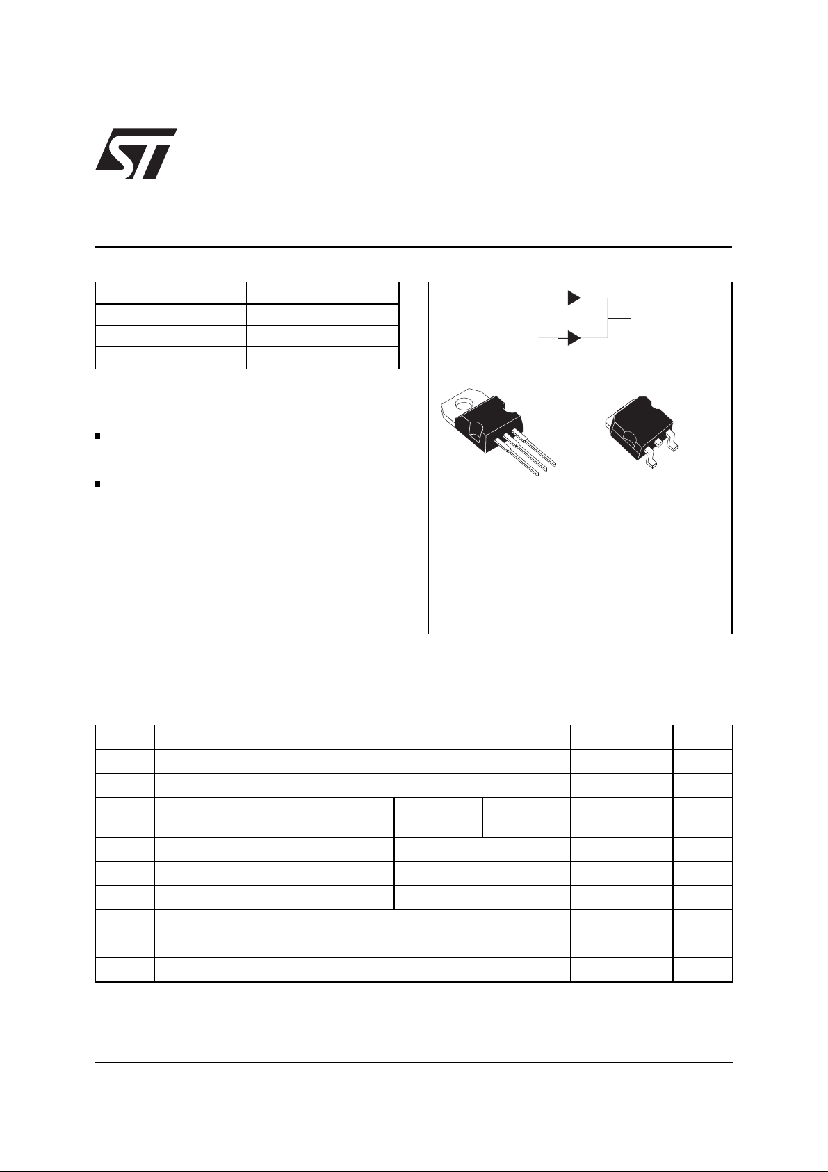
DESCR IPTION
Dual center tap Schottky rectifier suited to
Switched Mode Power Supplies and high
frequency DC to DC converters.
Packaged in TO-220AB and D
2
PAK, this device is
especially intended for use as a rectifier at the
secondary of 3.3V SMP S units.
A1
A2
A1
TO-220AB
STPS20L25CT
K
K
A2
K
A2
A1
D2PAK
STPS20L25CG
ABSOLUTE RATINGS
(limiting values, per diode)
Symbol Parameter Value Unit
V
RRM
I
F(RMS)
I
F(AV)
I
FSM
I
RRM
I
RSM
T
stg
Repetitive peak reverse voltage 25 V
RMS forward current 30 A
Average forward current Tc = 145°C
δ
= 0.5
Per diode
Per device
10
20
Surge non repetitive forward current tp = 10 ms S inusoidal 220 A
Repetitive peak reverse current tp=2 µs square F=1kHz 1 A
Non repetitive peak reverse current tp = 100 µs square 3 A
Storage temperature range - 65 to + 150
Tj Maximum operating junction temperature * 150 °C
dV/dt Critical rate of rise of reverse voltage 10000 V/µs
dPtot
* :
June 1999 - Ed : 3A
dTj
<
1
Rth(j−a
thermal runaway condition for a diode on its own heatsink
)
A
°
C
1/5
Page 2
STPS20L25CT/CG
THERMAL RE SISTA NC ES
Symbol Parameter Value Unit
R
th (j-c)
Junction to case Per diode 1.5
Total 0.8
R
th (c)
Coupling
0.1
When the diodes 1 and 2 are used simultaneously :
∆
Tj(diode 1) = P(diode1) x R
(Per diode) + P(diode 2) x R
th(j-c)
th(c)
STATIC ELECTRICAL CHARACTE RISTICS (per diode)
Symbol Tests conditions Tests conditions Min. Typ. Max. Unit
I
* Reverse leakage current Tj = 25°CV
R
= V
R
RRM
800
Tj = 125°C 125 250 m A
V
* Forward voltage drop Tj = 25°CI
F
Tj = 125°CI
Tj = 25°CI
Tj = 125°CI
= 10 A 0.46 V
F
= 10 A 0.30 0.35
F
= 20 A 0.56
F
= 20 A 0.41 0.48
F
°
C/W
µ
A
Pulse test : * tp = 380 µs, δ < 2%
To evaluate the maximum conduction losses use the following equation :
P = 0.22 x I
Fig.1 :
Average forward power dissipation versus
average forward current.
PF(av)(W)
5
4
3
2
1
0
01234567891011
F(AV)
δ = 0.05
+ 0.013 I
δ = 0.1
IF(av) (A)
F2(RMS )
δ = 0.2
δ = 0.5
δ
=tp/T
T
δ = 1
Fig.2 :
Average forward current versus ambient
temperature ( δ = 0.5).
IF(av)(A)
12
10
8
6
4
2
tp
0
0 25 50 75 100 125 150
δ
=tp/T
T
tp
Rth(j-a)=Rth(j-c)
Rth(j-a)=50°C/W
Tamb(°C)
2/5
Page 3

STPS20L25CT/CG
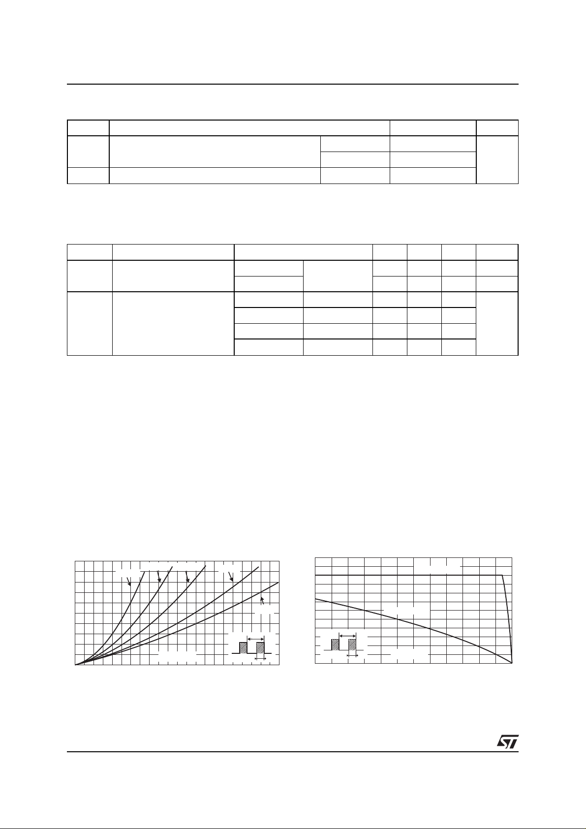
Fig.3 :
Non repetitive surge peak forward current
versus overload duration (maximum values).
IM(A)
200
180
160
140
120
100
80
60
I
M
40
20
0
1E-3 1E-2 1E-1 1E+0
Fig.5 :
t
δ
=0.5
t(s)
Reverse leakage current versus reverse
Tc=25°C
Tc=75°C
Tc=100°C
voltage applied (typical values).
IR(mA)
5E+2
1E+2
1E+1
1E+0
Tj=150°C
Tj=125°C
Fig.4 :
Relative variation of thermal impedance
junction to case versus pulse duration.
Zth(j-c)/Rth(j-c)
1.0
0.8
δ = 0.5
0.6
0.4
δ = 0.2
δ = 0.1
0.2
0.0
1.0E-4 1.0E-3 1.0E-2 1.0E-1 1.0E+0
Fig.6 :
Single pulse
Junction capacitance versus reverse
tp(s)
δ
=tp/T
T
tp
voltage applied (typical values).
C(nF)
5.0
1.0
F=1MHz
Tj=25°C
1E-1
1E-2
0 5 10 15 20 25
Fig.7 :
Forward voltage drop versus forward
Tj=25°C
VR(V)
current (maximum values).
IFM(A)
100.0
Typical values
10.0
1.0
0.1
0.0 0.1 0.2 0.3 0.4 0.5 0.6 0.7 0.8 0.9 1.0
Tj=150°C
Tj=25°C
Tj=125°C
VFM(V)
0.1
12 51020 50
Fig.8 :
Thermal resistance junction to ambient
versus copper surface under tab (Epoxy printed
circuit board FR4, copper thickness : 35 µm).
(STPS20L25G only)
Rth(j-a) (°C/W)
80
70
60
50
40
30
20
VR(V)
10
0
0 4 8 12 16 20 24 28 32 36 40
S(Cu) (cm²)
3/5
Page 4

STPS20L25CT/CG
PACKAGE MECHANICAL DAT A
2
PAK
D
E
L2
L
L3
A1
B2
B
G
* FLAT ZONE NO LESSTHAN 2mm
C2
DIMENSIONS
REF.
A
Millimeters Inches
Min. Max. Min. Max.
A 4.40 4.60 0.173 0.181
A1 2.49 2.69 0.098 0.106
A2 0.03 0.23 0.001 0.009
D
B 0.70 0.93 0.027 0.037
B2 1.14 1.70 0.045 0.067
C 0.45 0.60 0.017 0.024
C2 1.23 1.36 0.048 0.054
C
R
D 8.95 9.35 0.352 0.368
E 10.00 10.40 0.393 0.409
G 4.88 5.28 0.192 0.208
L 15.00 15.85 0.590 0.624
A2
L2 1.27 1.40 0.050 0.055
L3 1.40 1.75 0.055 0.069
M
*
V2
M 2.40 3.20 0.094 0. 126
R 0.40 typ. 0.016 typ.
V2 0° 8° 0° 8°
FOOTPRINT DIMENSIONS
16.90
10.30
8.90
4/5
(in millimeters)
1.30
3.70
Cooling method: by conduction ( method C)
5.08
Page 5

PACKAGE ME CHANICAL D AT A
TO-220AB
H2
Dia
L5
L6
L2
F2
F1
F
G1
G
L9
L4
STPS20L25CT/CG
DIMENSIONS
REF.
A
C
A 4.40 4.60 0.173 0.181
C 1.23 1.32 0.048 0.051
D 2.40 2.72 0.094 0.107
L7
E 0.49 0.70 0.019 0.027
F 0.61 0.88 0.024 0.034
F1 1.14 1.70 0.044 0.066
F2 1.14 1.70 0.044 0.066
D
G 4.95 5.15 0.194 0.202
G1 2.40 2.70 0.094 0.106
H2 10 10.40 0.393 0.409
L2 16.4 typ. 0.645 typ.
M
E
L4 13 14 0.511 0.551
L5 2.65 2.95 0.104 0.116
L6 15.25 15.75 0.600 0.620
L7 6.20 6.60 0.244 0.259
L9 3.50 3.93 0.137 0.154
M 2.6 typ. 0.102 typ.
Diam. 3.75 3.85 0.147 0.151
Millimeters Inches
Min. Max. Min. Max.
Cooling method : C
Recommended torque value : 0.55 m.N
Maximum torque value : 0.70 m.N
Ordering type Marking Package Weight Base qty
Delivery
mode
STPS20L25CT STPS20L25CT TO-220AB 2.23g 50 Tube
2
STPS20L25CG STPS20L25CG D
STPS20L25CG-TR STPS20L25CG D
PAK 1.48g 50 Tube
2
PAK 1.48g 1000 Tape & reel
Epoxy meets UL94,V0
Information furnished is believed to be accurate and reliable. However, STMicroelectronics assumes no responsibility for the consequences of
use of such information nor for any infringement of patents or other rights of third parties which may result from its use. No license is granted by
implication or oth erwise under any patent or patent rights of STMi croelectronics . Specifications mentioned i n this publication are subjec t to
change without notice. This publication supersedes and replaces all information previously supplied.
STMicroelectr oni cs products are n ot au thorized for use as critical components in life support devi ces or systems wi t hout express written approval of STMicroelectronics.
The ST logo is a registered trademark o f STMicroelectron ics
© 1999 STMicroelectronics - Printed in Italy - All rights reserved.
STMicroelectronics GROUP OF COMPANIES
Australia - Brazil - China - Finland - France - Germany - Hong Kong - India - Italy - Japan - Malaysia
Malta - Morocco - Singapore - Spain - Sweden - Switzerland - United Kingdom - U.S.A.
http://www.st.com
5/5
 Loading...