

Page 1

HIGH SPEED PROTECTION SWITCH
■ 24mA CMOS OUTPUT DRIV E CURRENT
■ LVTTL INPUT THRESHOLDS
■ CONTROLLEDSKEW BETWEEN DATA AND
CLOCK SIGNALS
■ LVDS INPUT-OUTPUT UP TO 155 MHZ
■ IMPROVED LATCH-UP IMMUNITY UP TO
300mA
DESCRIPTION
The STLVD112 is a low voltage differential to
LVTTL signal converter with enhanced l oop-back
and crosspoint features. The synchronous design
allows a phase alignment between a clock and its
data; this means a better BER (Bit Error Rate)
performance.
The advanced 0.35µm tec hnology makes the
STLVD112 suitable for data rates up to 200Mbit.
The main application field is SDH/SONE T telecom
infrastructure. The STLVD112 flexible switch
architecture makes it eas y to implement multiple
protection schemes in STM1 access systems.
Thanks to the flexibl e multiplexing allowed, it
becomes simple to redirect the data/c lock signal
coming from the faulty access card to the spare
card. In normal mode the STLVD11 2 c onv ert s the
differential data levels of the LVDS and related
STLVD112
TSSOP
clock s ignal from (to) the line interface in LVTTL
level signals to (from) the backpanel. In addition
the switch functions prevent the equipment from
line interface faults. In fact, it is possible to switch
the signals coming from a different line interface to
the local line interface or the signals from the loca l
line interface to a different line interface.
ORDERING CODES
Type
STLVD112BTR -40 to 85 °C TSSOP48 (Tape & Reel) 1000 parts per reel
STLVD112CTR 0 to 70 °C TSSOP48 (Tape & Reel) 1000 parts per reel
Temperature
Range
Package Comments
1/11April 2003
Page 2
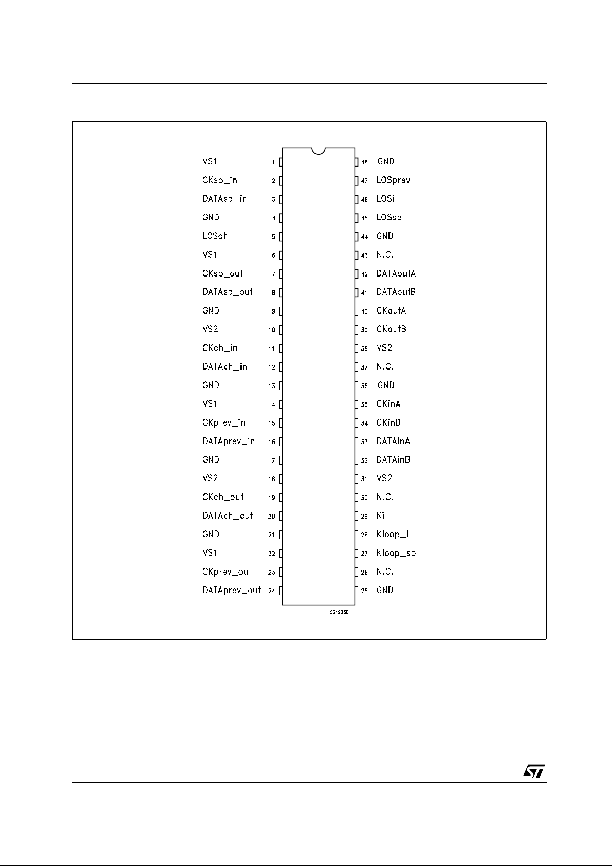
STLVD112
PIN CONFIGURATION
2/11
Page 3
PIN DESCRIPTION
PlN N° SYMBOL NAME AND FUNCTION
1, 6, 14, 22 VS1 Main Power Supply
2 CKsp_in LVTTL Clock Input
3 DATAsp_in LVTTL Data Input
4, 9, 13, 17, 21,
25, 36, 44, 48
5 LOSch Control Output
7 CKsp_out LVTTL Clock Output
8 DATAsp_out LVTTL Data Output
10, 18, 31, 38 VS2 Second Power Supply
11 CKch_in LVTTL Clock Input
12 DATAch_in LVTTL Data Input
15 CKprev_in LVTTL Clock Input
16 DATAprev_in LVTTL Data Input
19 CKch_out LVTTL Clock Output
20 DATAch_out LVTTL Data Output
23 CKprev_out LVTTL Clock Output
24 DATAprev_out LVTTL Data Output
26, 30, 37, 43 N.C. Not Connected
27 Kloop_sp Control Input
28 Kloop_I Control Input
29 Ki Control Input
32 DATAinB LVDS Data Input 33 DATAinA LVDS Data Input +
34 CKinB LVDS Clock Input 35 CKinA LVDS Clock Input +
39 CKoutB LVDS Clock Output 40 CKoutA LVDS Clock Output +
41 DATAoutB LVDS Data Output 42 DATAoutA LVDS Data Output +
45 LOSsp Control Output
46 LOSi Control Input
47 LOSprev Control Input
GND
Ground
STLVD112
TRUTH TABLES FOR THE FIVE MUX
INPUTS OUTPUT
Ki Kloop_sp Kloop_i DATA_out
LOW X X DATAch_in
HIGH X X DATAsp_in
INPUTS OUTPUT
Ki Kloop_sp Kloop_i DATAch_out
X X LOW DATAin
X X HIGH DATAch-in
3/11
Page 4
STLVD112
INPUTS OUTPUT
Ki Kloop_sp Kloop_i DATAsp_out
LOW LOW X DATAprev_in
HIGH LOW X DATA_in
X HIGH X DATAsp_in
INPUTS OUTPUT
Ki Kloop_sp Kloop_i LOSch
X X LOW LOSi
X X HIGH LOW
INPUTS OUTPUT
Ki Kloop_sp Kloop_i LOSsp
LOW LOW X LOSprev
HIGH LOW X LOSi
X HIGH X LOW
ABSOLUTE MAXIMUM RATINGS
Symbol Parameter Value Unit
VS1, VS2 Supply Voltage
VS2 Supply Voltage
V
V
DC Input Voltage
I
DC Output Voltage
O
Iik DC Input Diode Clamp Current ±20 mA
Iok DC Output Diode Clamp Current ±20 mA
I
T
T
Absolute Maximum Ratings are those values beyond which damage to the device may occur. Functional operation under these conditions is
not implied.
DC Output Current
O
Lead Temperature (10sec)
L
Storage Temperature Range
stg
-0.3 to 4.6 V
-0.3 to (VS1 + 0.3) V
-0.3 to (VS1 + 0.3) V
-0.3 to (VS1 + 0.3) V
±50 mA
300 °C
-65 to 150 °C
RECOMMENDED OPERATING CONDITIONS
Symbol Parameter Value Unit
VS1, VS2 Supply Voltage
VS2 Supply Voltage
V
V
DC Input Voltage
I
DC Output Voltage
O
Top Operating Temperature -45 to 85 °C
dt/dv Maximum Input Rise and Fall Time 10 ns/V
4/11
3 to 3.6 V
3 to (VS1 + 0.3) V
0 to VS1 V
0 to VS1 V
Page 5

STLVD112
ELECTRICAL CHARACTERISTICS (Over r ec ommended operating conditions, unless otherwise noted.
All typical values are at T
Symbol Parameter Test Conditions
Low Level Output Voltage I
V
OL
High Level Output Voltage I
V
OH
Low Level Input Thresholds V
V
IL
High Level Input Thresholds V
V
IH
I
Input Leakage Current VIN= GND or V
IN
Quiescent Supply Current VIN= GND or V
I
CC
LVDS DRIVER ELECTRICAL CHARACTERISTICS (Over recomm ended operating conditions, unless
otherwise noted. All typical values are at T
Symbol Parameter Test Conditions
Differential Output Voltage RL= 100 Ω 247 364 454 mV
OD
Change in differential output voltage
OD
between logic states
Steady-state common-mode output
voltage
Change in steady-state common-
mode output voltage between logic
State
Peak-to-Peack common-mode output
voltage
Short Circuit Output Current V
SC
Power Off Output Current VCC=0,VO= 2.4V -1 1 µA
∆V
V
∆V
∆V
V
OC(SS)
OC(SS)
OC(PP)
I
I
OFF
=25°C and VS1,VS2=3.3V)
A
= 24 mA 0.2 0.4 V
OUT
=24mA VSI-0.5 VSI-0.3 V
OUT
= 0.1V or VS1- 0.1 0 0.8 V
OUT
= 0.1V or VS1- 0.1 2 V
OUT
CC
CC
= 155MHz 110
f
CLOCK
=25°C and VS1,VS2=3.3V)
A
or V
O(Y)
=0 ±12
V
OD
Value
Min. Typ. Max.
SI
-1 1 µA
15 mA
Value
Min. Typ. Max.
-50 50 mV
1 1.15 1.30 V
-50 50 mV
100 150 mV
= 0 -24 -4 mA
O(Z)
Unit
V
Unit
LVDS RECEIVER ELECTRICAL CHARACT ERISTICS (Over recommended operating conditions,
unless otherwise noted. All typical values are at T
Symbol Parameter Test Conditions
V
V
|V
Positive-going Differential Input
ITH+
Voltage Threshold
Negative-going Differential Input
ITH-
Voltage Threshold
| Magnitude of Differential Input
ID
Voltage
V
Common-mode Input Voltage 0.5
IC
=25°C and VS1,VS2=3.3V)
A
Min. Typ. Max.
-100 mV
0.1 0.6 V
|V
Value
100 mV
2.4-0.5
|
ID
|VID|
V
CC
-1
Unit
V
5/11
Page 6
STLVD112
LVDS SWITCHING TIMING CHARACTERISTICS (Over recommended operating conditions, unless
otherwise noted. All typical v alues are at T
Symbol Parameter Test Conditions
Minimum Pulse Width <1 ns
t
W
AC LVTTL IN LVTTL OUT (Over recommended op erating conditions, unless otherwise noted. All typical
values are at T
Symbol Parameter Test Conditions
t
PLH
t
PHL
t
TLH
t
THL
f
opr
=25°C and VS1,VS2=3.3V)
A
Propagation Delay Time, low-to-highlevel output (50% to 50%)
Propagation Delay Time, high-to-lowlevel output (50% to 50%)
Transition Time, low-to-high-level
output (10% to 90%)
Transition Time, high-to-low-level
output (90% to 10%)
Operative frequency 100 155 200 MHz
=25°C and VS1,VS2=3.3V)
A
Measured with VIN=0 to 2.5V,
f
= 1MHz, f
CLOCK
t
= 0.4ns, +Duty Cycle=50%
r=tf
t
PHL,tPLH
are referred to output
DATA
= 0.5MHz
clock transitions.
Value
Unit
Min. Typ. Max.
Value
Unit
Min. Typ. Max.
2.4 3.9 5.6 ns
2.5 4.2 5.3 ns
0.7 1.3 1.6 ns
0.7 1.1 1.3 ns
AC CONTROL OUTPUT (LOSsp, LOSch) (Over recommended operating conditions, unless otherwise
noted. All typical values are at T
Symbol Parameter Test Conditions
t
t
t
t
Propagation Delay Time, low-to-high-
PLH
level output (50% to 50%)
Propagation Delay Time, high-to-low-
PHL
level output (50% to 50%)
Transition Time, low-to-high-level
TLH
output (10% to 90%)
Transition Time, high-to-low-level
THL
output (90% to 10%)
=25°C and VS1,VS2=3.3V)
A
Measured with VIN=0 to 2.5V,
f
= 1MHz, f
CLOCK
t
= 0.4ns, +Duty Cycle=50%
r=tf
t
PHL,tPLH
are referred to output
clock transitions.
DATA
Value
Unit
Min. Typ. Max.
2.4 3.6 4.4 ns
= 0.5MHz
2.4 3.4 4.2 ns
0.9 1.9 2.3 ns
0.7 1.0 1.2 ns
AC LVTTL IN LVDS OUT (Over recommended operating conditions, unless otherwise note d. All typical
values are at T
Symbol Parameter Test Conditions
t
PLH
t
PHL
t
TLH
t
THL
f
opr
=25°C and VS1,VS2=3.3V)
A
Value
Unit
Min. Typ. Max.
Propagation Delay Time, low-to-highlevel output (50% to 50%)
Propagation Delay Time, high-to-lowlevel output (50% to 50%)
Transition Time, low-to-high-level
Measured with VIN=0 to 2.5V,
f
= 1MHz, f
CLOCK
t
= 0.4ns, +Duty Cycle=50%
r=tf
t
PHL,tPLH
are referred to output
DATA
= 0.5MHz
clock transitions.
2.8 3.8 4.7 ns
2.6 3.4 4.1 ns
0.4 0.5 0.6 ns
output (20% to 80%)
Transition Time, high-to-low-level
0.4 0.6 0.7 ns
output (80% to 20%)
Operative frequency 100 155 200 MHz
6/11
Page 7
STLVD112
AC LVDS IN LVTTL O UT (Over recommended operating conditions, unless otherwise noted. All typical
values are at T
Symbol Parameter Test Conditions
t
PLH
t
PHL
t
TLH
t
THL
f
opr
=25°C and VS1,VS2=3.3V)
A
Value
Unit
Min. Typ. Max.
Propagation Delay Time, low-to-highlevel output (50% to 50%)
Propagation Delay Time, high-to-lowlevel output (50% to 50%)
Transition Time, low-to-high-level
output (10% to 90%)
Transition Time, high-to-low-level
V
= 400mV
DIFF
Measured with V
f
= 1MHz, f
CLOCK
= 0.4ns, +Duty Cycle=50%
t
r=tf
t
PHL,tPLH
ICM
DATA
are referred to output
clock transitions
=1.2V,
= 0.5MHz
4.3 5.6 6.9 ns
4.1 5.4 6.7 ns
0.7 0.9 1.1 ns
0.8 1.0 1.3 ns
output (90% to 10%)
Operative frequency 100 155 200 MHz
LVTTL IN LVTTL OUT (V
T
=25°C)
A
=3to3.6VTA= -45 to 80°C, unless otherwise noted. Typical values are at
CC
Value
Symbol Parameter Test Conditions
Min. Typ. Max.
Setup Time f = 10MHz, V
t
s
Hold Time 1 ns
t
H-
V
V
DIFF
INTTL
= 400mV,
= 0 to 2.5V
ICM
= 1.2 V
1ns
LVTTL IN LVDS OUT (Over recommended operating conditions, unless otherwise noted. All typical
values are at T
Symbol Parameter Test Conditions
t
s
t
H-
=25°C and VS1,VS2=3.3V)
A
Value
Min. Typ. Max.
Setup Time f = 10MHz, V
V
= 400mV,
Hold Time 1 ns
V
DIFF
INTTL
= 0 to 2.5V
ICM
= 1.2 V
1ns
LVDS IN LVTTL OUT (Over recommended operating conditions, unless otherwise noted. All typical
values are at T
Symbol Parameter Test Conditions
t
s
t
H-
=25°C and VS1,VS2=3.3V)
A
Value
Min. Typ. Max.
Setup Time f = 10MHz, V
V
= 400mV,
Hold Time 1 ns
V
DIFF
INTTL
= 0 to 2.5V
ICM
= 1.2 V
1.5 ns
Unit
Unit
Unit
7/11
Page 8

STLVD112
LOGIC DIAGRAM
8/11
Page 9

STLVD112
TSSOP48 MECHANICAL DATA
mm. inch
DIM.
MIN. TYP MAX. MIN. TYP. MAX.
A 1.2 0.047
A1 0.05 0.15 0.002 0.006
A2 0.9 0.035
b 0.17 0.27 0.0067 0.011
c 0.09 0.20 0.0035 0.0079
D 12.4 12.6 0.488 0.496
E 8.1 BSC 0 .31 8 BSC
E1 6.0 6.2 0.236 0.244
e 0.5 BSC 0.0197 BSC
K0˚ 8˚0˚ 8˚
L 0.50 0.75 0.020 0.030
A2
A
A1
b
e
D
K
c
E1
L
E
PIN 1 IDENTIFICATION
1
7065588C
9/11
Page 10
STLVD112
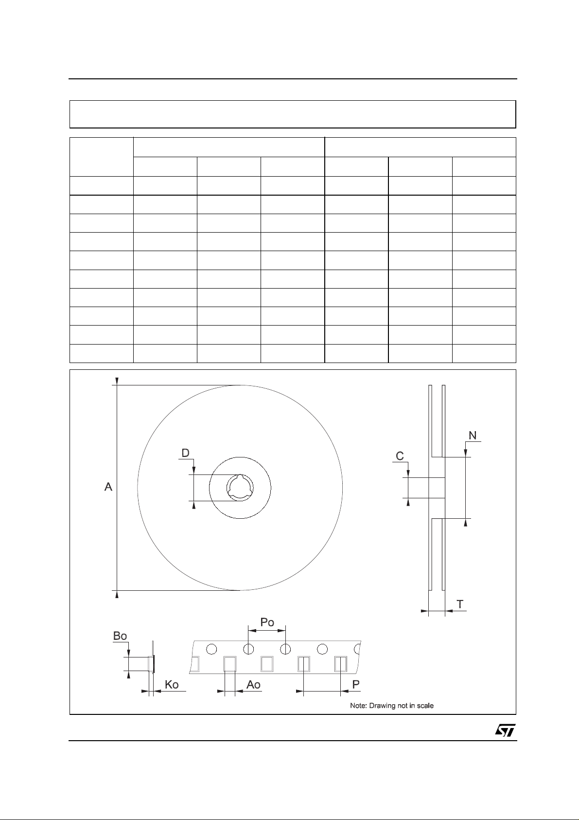
Tape & Reel TSSOP48 MECHANICAL DATA
mm. inch
DIM.
MIN. TYP MAX. MIN. TYP. MAX.
A 330 12.992
C 12.8 13.2 0.504 0.519
D 20.2 0.795
N 60 2.362
T 30.4 1.197
Ao 8.7 8.9 0.343 0.350
Bo 13.1 13.3 0.516 0.524
Ko 1.5 1.7 0.059 0.067
Po 3.9 4.1 0.153 0.161
P 11.9 12.1 0.468 0.476
10/11
Page 11

STLVD112
Information furnished is believed to be accurate and reliable. However, STMicroelectronics assumes no responsibility for the
consequences of use o f suc h inf ormat ion n or f or an y infr ingeme nt of paten ts or oth er ri gh ts of third part ies whic h may resul t f rom
its use. No license is granted by implication or otherwise under any patent or patent rights of STMicroelectronics. Specifications
mentioned in this publication are subject to change without notice. This publication supersedes and replaces all information
previously supplied. STMicroelectronics products are not authorized for use as critical components in life support devices or
systems without express written approval of STMicroelectronics.
Australia - Brazil - Canada - China - Finland - France - Germany - Hong Kong - India - Israel - Italy - Japan - Malaysia - Malta - Morocco
© The ST logo is a registered trademark of STMicroelectronics
© 2003 STMicroelectronics - Printed in Italy - All Rights Reserved
STMicroelectronics GROUP OF COMPANIES
Singapore - Spain - Sweden - Switzerland - United Kingdom - United States.
© http://www.st.com
11/11
 Loading...