

Page 1
STLC60135
TOSCA
DTM modem for ADSL, compatible with the
followingstandards:
– ANSI T1.413 Issue 2
– ITU-T G.992.1(G.dmt)
– ITU-T G.992.2(G.lite)
Samechip for both ATU-C and ATU-R
Supportseither ATM (Utopia level1 & 2) or bit-
stream interface
16 bit multiplexed microprocessor interface (lit-
tle and bigendiancompatibility)
Analog Front End management
Dual latencypaths: fast and interleaved
ATM’s PHY layer: cell processing (cell deline-
ation, cell insertion,HEC)
ADSL’soverheadmanagement
Reed Solomonencode/decode
Trellis encode/decode(Viterbi)
DMT mapping/ demapping over 256 carriers
Fine (2ppm) timing recover using Rotor and
AdaptativeFrequencyDomainEqualizing
TimeDomain Equalization
Frontend digitalfilters
0.35µmHCMOS6Technology
144 pin PQFPpackage
PowerConsumption1 Watt at 3.3V
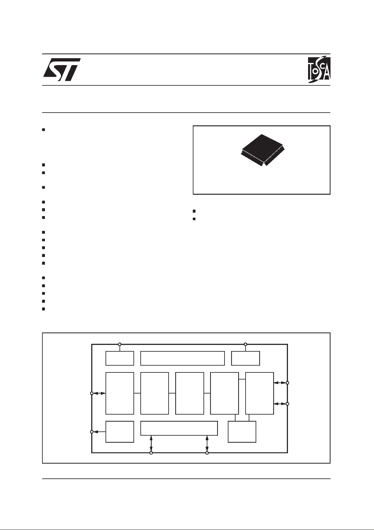
Figure 1. Block Diagram
ADSL DMT TRANSCEIVER
PQFP144
ORDERING NUMBER: STLC60135
Applications
ATU-C:
ATU-R:
DSLAM,Routersat Central Office
Routers at SOHO, stand-alone mo-
dems, PC motherboards
GeneralDescription
The STLC60135 is the DMT modem and ATM
framerof theSTMicroelectronicsTosca chipset.
When coupled with STLC60134 analog front-end
and an external controller running dedicated firmware, the product fulfils ANSI T1.413 “Issue 2”
DMT ADSL specification.
The STLC60135 may be used at both ends of
ADSL loop: ATU-C and ATU-R. The chip supports UTOPIA level 1 and UTOPIA level 2 interface and a non ATM synchronous bit-stream interface.
AFE
INTERFACE
AFE
CONTROL
September 1999
TEST SIGNALS CLOCK
TEST
MODULE
DSP
FRONT-END
AFE
CONTROL
INTERFACE
CONTROLLER BUS GENERAL PURPOSE I/Os
DATA SYMBOLTIMING UNIT VCXO
FFT/IFFT
ROTOR
CONTROLLER INTERFACE
TRELLIS
CODING
MAPPER/
DEMAPPER
GENERIC
TC
REED/
SOLOMON
ATM
SPECIFIC
TC
INTERFACE
MODULE
STM
UTOPIA
D98TL315
1/25
Page 2
STLC60135
The STLC60135 can be splitted up into two different sections. The physical one performs the DMT
modulation, demodulation,Reed-Solomonencoding, bit interleavingand 4D trellis coding.
The ATM section embodies framing functions for
the generic and ATM Transmission Convergence
(TC) layers. The generic TC consists of data
scrambling and Reed Solomon error corrections,
with and without interleaving.
The STLC60135 is controlled and programmed
by an external controller (ADSL Transceiver Controller, ATC) that sets the programmable coefficients.
Transient Energy Capabilities
ESD
ESD (Electronic Discharged) tests have been
performed for the HumanBody Model (HBM) and
for the Charged Device Model (CDM).
The pins of the device are to be able to withstand
minimum 1500V for the HBM and minimum250V
for CDM.
Latch-up
The maximum sink or sourcecurrentfrom any pin
is limitedto 100mA to prevent latch-up.
The firmware controls the initialization phase and
carriesout the consequentadaptationoperations.
ABSOLUTE MAXIMUM RATINGS
Symbol Parameter Min Typ Max Unit
V
DD
P
tot
T
amb
Supply Voltage 3.0 3.3 3.6 V
Total Power Dissipation 900 1400 mW
Ambient Temperature 1m/s airflow -40 85 °C
Figure 2. Pin Connection
AFTXD_0
IDDq
VDD
AFTXED_3
VSS
AFTXED_2
AFTXED_1
AFTXED_0
VDD
CTRLDATA
52 53
VDD
U_RXDATA_7
U_RX_ADDR_0
U_RX_ADDR_1
MCLK
CLWD
AFRXD_3
VSS
AFRXD_2
124 122123 121120119118117
54 55 56 57 58 59
VSS
GP_IN0
U_RX_ADDR_2
U_RX_ADDR_3
U_RX_ADDR_4
AFRXD_1
AFRXD_0
VDD
VSS
VDD
GP_IN1
PDOWN
GP_OUT
TESTSE
62 63 64 65 66 67
60 61
VDD
U_TX_REFB
U_RX_REFB
TRSTB
VSS
116 114115 113112111110109
U_RXCLK
U_RXSOC
AFTXD_1
VSS
AFTXD_2
AFTXD_3
VDDVDD
140
141
1
VSS
2
AD_0
3
AD_1
4
AD_2
5
VDD
6
AD_3
7
AD_4
8
VSS
9
AD_5
10
AD_6
VDD
12
AD_7
13
AD_8
14
AD_9
15
VSS
16
AD_10
17
AD_11
18
VDD
19
AD_12
20
VSS
21
PCLK
22
VDD
23
AD_13
24
AD_14
25
AD_15
26
VSS
27
BE1
28
ALE
29
VDD
30
CSB
31
WR_RDB
32
RDYB
OBC_TYPE
33
34
INTB
35
RESETB
36
VSS VSS
37 38 39 40
U_RXDATA_0
41 42 43 44 45
VSS
U_RXDATA_1
135134133132 130131 129128127126125
137142143144
138
139
136
461147 48 49 50 51
VSS
VDD
U_RXDATA_3
U_RXDATA_4
U_RXDATA_5
U_RXDATA_2
U_RXDATA_6
TCK
VDD
TMS
68 69 70
VSS
U_RXCLAV
U_RXENBB
TDI
TDO
U_TXCLK
U_TXSOC
SLT_FRAME_S
SLT_REQ_S
VSS
108
VDD
107
SLT_REQ_F
106
SLT_DAT_S0
105
SLT_DAT_S1
104
SLT_DAT_F0
103
SLT_DAT_F1
102
VSS
101
SLT_FRAME_F
100
SLAP_CLOCK
99
SLR_VAL_F
98
SLR_DAT_F0
97
SLR_DAT_F1
96
SLR_VAL_S
95
VDD
94
SLR_DAT_S0
93
SLR_DAT_S1
92
SLR_FRAME_S
91
VSS
90
SLR_FRAME_F
89
U_TX_ADDR_0
88
U_TX_ADDR_1
87
U_TX_ADDR_2
86
VDD
85
U_TX_ADDR_3
84
U_TX_ADDR_4
83
U_TX_DATA_0
82
U_TX_DATA_1
81
VDD
80
U_TX_DATA_2
79
U_TX_DATA_3
78
U_TX_DATA_4
77
U_TX_DATA_5
76
VDD
75
U_TX_DATA_6
74
U_TX_DATA_7
73
71
72
VDD
D98TL367B
U_TXENBB
U_TX_CLAV
2/25
Page 3

PIN FUNCTIONS
Pin Name Type Supply Driver BS Function
1 VSS 0V Ground
2 AD_0 B VDD BD8SCR B Data 0
3 AD_1 B VDD BD8SCR B Data 1
4 AD_2 B VDD BD8SCR B Address / Data 2
5 VDD (V
6 AD_3 B VDD BD8SCR B Address / Data 3
7 AD_4 B VDD BD8SCR B Address / Data 4
8 VSS 0V Ground
9 AD_5 B VDD BD8SCR B Address / Data 5
10 AD_6 B VDD BD8SCR B Address / Data 6
11 VDD (V
12 AD_7 B VDD BD8SCR B Address / Data 7
13 AD_8 B VDD BD8SCR B Address / Data 8
14 AD_9 B VDD BD8SCR B Address / Data 9
15 VSS 0V Ground
16 AD_10 B VDD BD8SCR B Address / Data 10
17 AD_11 B VDD BD8SCR B Address / Data 11
18 VDD (V
19 AD_12 B VDD BD8SCR B Address / Data 12
20 VSS 0V Ground
21 PCLK I VDD IBUF I Processor clock
22 VDD (V
23 AD_13 B VDD BD8SCR B Address / Data 13
24 AD_14 B VDD BD8SCR B Address / Data 14
25 AD_15 B VDD BD8SCR B Address / Data 15
26 VSS 0V Ground
27 BE1 I VDD IBUF I Address 1
28 ALE I VDD IBUF C Address Latch
29 VDD (V
30 CSB I VDD IBUF I Chip Select
31 WR_RDB I VDD IBUF I Specifies the direction of the access cycle
32 RDYB OZ VDD BT4CR O Controls the ATC bus cycle termination
33 OBC_TYPE I-PD VDD IBUF I ATC Mode Selection (0 = i960; 1 = generic)
34 INTB O VDD IBUF O Requests ATC interrupt service
35 RESETB I VDD IBUF I Hard reset
36 VSS 0V Ground
37 VDD (V
38 U_RxData_0 OZ VDD BD8SRC B Utopia RX Data 0
39 U_RxData_1 OZ VDD BD8SRC B Utopia RX Data 1
40 VSS 0V Ground
41 U_RxData_2 OZ VDD BD8SRC B Utopia RX Data 2
42 U_RxData_3 OZ VDD BD8SRC B Utopia RX Data 3
43 VDD (V
+ 3.3V) Power Supply
SS
SS + 3.3V) Power Supply
SS + 3.3V) Power Supply
+ 3.3V) Power Supply
SS
SS + 3.3V) Power Supply
+ 3.3V) Power Supply
SS
+ 3.3V) Power Supply
SS
STLC60135
3/25
Page 4

STLC60135
PIN FUNCTIONS (continued)
Pin Name Type Supply Driver BS Function
44 U_RxData_4 OZ VDD BD8SRC B Utopia RX Data 4
45 U_RxData_5 OZ VDD BD8SRC B Utopia RX Data 5
46 VSS 0V Ground
47 U_RxData_6 OZ VDD BD8SRC B Utopia RX Data 6
48 U_RxData_7 OZ VDD BD8SRC B Utopia RX Data 7
49 VDD (V
50 U_RxADDR_0 I VDD IBUF I Utopia RX Address 0
51 U_RxADDR_1 I VDD IBUF I Utopia RX Address 1
52 U_RxADDR_2 I VDD IBUF I Utopia RX Address 2
53 U_RxADDR_3 I VDD IBUF I Utopia RX Address 3
54 VSS 0V Ground
55 U_RxADDR_4 I VDD IBUF I Utopia RX Address 4
56 GP_IN_0 I-PD VDD IBUFDQ I General purpose input 0
57 VDD (V
58 GP_IN_1 I-PD VDD IBUFDQ I General purpose input 1
59 VSS 0V Ground
60 U_RxRefB O VDD IBUF O 8kHz clock to ATM device
61 U_TxRefB I VDD BT4CR I 8kHz clock from ATM device
62 VDD (V
63 U_Rx_CLK I VDD IBUF Utopia RX Clock
64 U_Rx_SOC OZ VDD BD8SCR Utopia RX Start of Cell
65 U_RxCLAV OZ VDD BD8SCR Utopia RX Cell Available
66 U_RxENBB I VDD IBUF Utopia RX Enable
67 VSS 0V Ground
68 U_Tx_CLK I VDD IBUF Utopia TX Clock
69 U_Tx_SOC I VDD IBUF Utopia TX Start of Cell
70 U_TxCLAV OZ VDD BD8SCR Utopia TX Cell Available
71 U_TxENBB I VDD IBUF Utopia TX Enable
72 VDD (V
73 VSS 0V Ground
74 U_TxData_7 I VDD IBUF I Utopia TX Data 7
75 U_TxData_6 I VDD IBUF I Utopia TX Data 6
76 VDD (V
77 U_TxData_5 I VDD IBUF I Utopia TX Data 5
78 U_TxData_4 I VDD IBUF I Utopia TX Data 4
79 U_TxData_3 I VDD IBUF I Utopia TX Data 3
80 U_TxData_2 I VDD IBUF I Utopia TX Data 2
81 VDD (V
82 U_TxData_1 I VDD IBUF I Utopia TX Data 1
83 U_TxData_0 I VDD IBUF I Utopia TX Data 0
84 U_TxADDR_4 I VDD IBUF I Utopia TX Address 4
85 U_TxADDR_3 I VDD IBUF I Utopia TX Address 3
86 VDD (V
87 U_TxADDR_2 I VDD IBUF I Utopia TX Address 2
88 U_TxADDR_1 I VDD IBUF I Utopia TX Address 1
89 U_TxADDR_0 I VDD IBUF I Utopia TX Address 0
90 SLR_ FRAME_F O VDD BT4CR Frame Identifier Fast
91 VSS 0V Ground
SS + 3.3V) Power Supply
+ 3.3V) Power Supply
SS
+ 3.3V) Power Supply
SS
SS + 3.3V) Power Supply
+ 3.3V) Power Supply
SS
+ 3.3V) Power Supply
SS
+ 3.3V) Power Supply
SS
4/25
Page 5

PIN FUNCTIONS (continued)
Pin Name Type Supply Driver BS Function
92 SLR_FRAME_S O VDD BT4CR Receive Frame Identifier Interleaved
93 SLR_DATA_S_1 O VDD BT4CR Receive Data Interleave 1
94 SLR_DATA_S_0 O VDD BT4CR Receive Data Interleave 0
95 VDD (V
96 SLR_VAL_S O VDD BT4CR Receive Data Valid Indicator Interleaved
97 SLR_DATA_F_1 O VDD BT4CR Receive Data Fast 1
98 SLR_DATA_F_0 O VDD BT4CR Receive Data Fast 0
99 SLR_VAL_F O VDD BT4CR Receive Data Valid Indicator Fast
100 SLAP_CLOCK O VDD BT4CR Clock for SLAP I/F
101 SLT_FRAME_F O VDD BT4CR Transmit Start of frame Indicator Fast
102 VSS 0V Ground
103 SLT_DATA_F_1 I VDD IBUFDQ Transmit Data Fast 1
104 SLT_DATA_F_0 I VDD IBUFDQ Transmit Data Fast 0
105 SLT_DATA_S_1 I VDD IBUFDQ Transmit Data Interleave 1
106 SLT_DATA_S_0 I VDD IBUFDQ Transmit Data Interleave 0
107 SLT_REQ_F O VDD BT4CR Transmit Byte Request Fast
108 VDD (V
109 VSS 0V Ground
110 SLT_REQ_S O VDD BT4CR Transmit Byte Request Interleaved
111 STL_FRAME_S O VDD BT4CR Transmit Start of frame Indication Interleaved
112 TDI I-PU VDD IBUFUQ JTAG I/P
113 TDO OZ VDD BT4CR JTAG O/P
114 TMS I-PU VDD IBUFUQ JTAG Made Select
115 VDD (V
116 TCK I-PD VDD IBUFDQ JTAG Clock
117 VSS 0V Ground
118 TRSTB I-PD VDD IBUFDQ JTAG Reset
119 TESTSE I VDD IBUF none Enables scan test mode
120 GP_OUT O VDD BD8SCR O General purpose output
121 PDOWN O VDD BT4CR O Power down analog front end (Reset)
122 VDD (V
123 AFRXD_0 I VDD IBUF I Receive data nibble
124 AFRXD_1 I VDD IBUF I Receive data nibble
125 AFRXD_2 I VDD IBUF I Receive data nibble
126 AFRXD_3 I VDD IBUF I Receive data nibble
127 VSS 0V Ground
128 CLWD I VDD IBUF I Start of word indication
129 MCLK I VDD IBUF C Master clock
130 CTRLDATA O VDD BT4CR O Serial data Transmit channel
131 VDD (V
132 AFTXED_0 O VDD BT4CR O Transmit echo nibble
133 AFTXED_1 O VDD BT4CR O Transmit echo nibble
134 VSS 0V Ground
135 AFTXED_2 O VDD BT4CR O Transmit echo nibble
136 AFTXED_3 O VDD BT4CR O Transmit echo nibble
137 VDD (V
138 IDDq I VDD IBUF none Testpin, active high
SS + 3.3V) Power Supply
+ 3.3V) Power Supply
SS
SS + 3.3V) Power Supply
+ 3.3V) Power Supply
SS
+ 3.3V) Power Supply
SS
SS + 3.3V) Power Supply
STLC60135
5/25
Page 6
STLC60135
PIN FUNCTIONS (continued)
Pin Name Type Supply Driver BS Function
139 AFTXD_0 O VDD BT4CR O Transmit data nibble
140 AFTXD_1 O VDD BT4CR O Transmit data nibble
141 VSS 0V Ground
142 AFTXD_2 O VDD BT4CR O Transmit data nibble
143 AFTXD_3 O VDD BT4CR O Transmit data nibble
144 VDD (V
I/O DRIVER FUNCTION
Driver Function
BD4CR CMOS bidirectional, 4mA, slew rate control
BD8SCR CMOS bidirectional, 8mA, slew rate control, Schmitt trigger
IBUF CMOS input
IBUFDQ CMOS input, pull down, IDDq control
IBUFUQ CMOS input, pull up, IDDq control
PIN SUMMARY
Mnemonic Type BS Type Signals Function
SS + 3.3V) Power Supply
Power Supply
VDD (VSS+ 3.3V) Power Supply
VSS 0V Ground
ATC Interface
ALE I C 1 Used to latch the address of the internal register to be accessed
PCLK I I 1 Processor clock
CSB I I 1 Chip selected to respond to bus cycle
BE1 I I 1 Address 1 (notmultiplexed)
WR_RDB I I 1 Specifies the direction of the access cycle
RDYB OZ O 1 Controls the ATC bus cycle termination
INTB O O 1 Requests ATC interrupt service
AD IO B 16 MultiplexedAddress/Data bus
OBC_TYPE I-PD I 1 Select betweeni960 (0) or generic (1) controller interface
Test Access Part Interface
TDI I-PU 1 refer to section
TDO OZ 1
TCK I-PD 1
TMS I-PU 1
TRSTB I-PD 1
Analog Front End Interface
AFRXD I I 4 Receive data nibble
AFTXD O O 4 Transmit data nibble
AFTXED O O 4 Transmit echo nibble
CLWD I I 1 Start of word indication
PDOWN O O 1 Power down analog front end
CTRLDATA O O 1 Serial data transmit channel
MCLK I C 1 Master clock
6/25
Page 7
PIN SUMMARY(continued)
Mnemonic Type BS Type Signals Function
ATM UTOPIA Interface
U_RxData OZ B 8 Receive interface Data
U_TxData I I 8 Transmit interface Data
U_RxADDR I I 5 Receive interface Address
U_TxADDR I I 5 Transmit interface Address
U_RxCLAV OZ O 1 Receive interface Cell Available
U_TxCLAV OZ O 1 Transmit interface Cell Available
U_RxENBB I-TTL I 1 Receive interface Enable
U_TxENBB I-TTL I 1 Transmit interface Enable
U_RxSOC OZ O 1 Receive interface Start of Cell
U_TxSOC I-TTL I 1 Transmit interface Start of Cell
U_RxCLK I-TTL C 1 Receive interface Utopia Clock
U_TxCLK I-TTL C 1 Transmit interface Utopia Clock
U_RxRefB O O 1 8kHz reference clock to ATM device
U_TxRefB I-TTL I 1 8kHz reference clock from ATM device
ATM SLAP Interface
SLR_VAL_S O 1
SLR_VAL_F O 1
SLR_DATA_S O 2
SLR_DATA_F O 2
SLT_REQ_S O 1
SLT_REQ_F O 1
SLT_DATA_S I 2
SLT_DATA_F I 2
SLAP_CLOCK O 1
SLR_FRAME_I O 1
SLT_FRAME_I O 1
SLR_FRAME_F O 1
SLT_FRAME_F O 1
STLC60135
Miscellaneous
GP_IN I-PD I 2 General purpose input
GP_OUT O O 1 General purpose output
RESETB I I I Hard reset
TESTSE I none none Enable scan test mode
IDDq I none none Test pin, active high
I = Input, CMOS levels
I-PU = Input with pull-up resistance, CMOS levels
I-PD = Input with pull-down resistance, CMOS levels
I-TTL = Input TTL levels
O = Push-pull output
OZ = Push-pull output with high-impedance state
IO = Input / Tristate Push-pull output
BS cell = Boundary-Scan cell
I = Input cell
O = Output cell
B = Bidirectional cell
C = Clock
7/25
Page 8
STLC60135
Main Block Description
The following drawings describe the sequence of
functionsperformed by the chip.
DSP Front-End
The DSP Front-End contains 4 parts in the receive direction: the Input Selector, the Analog
Front-End Interface, the Decimator and the Time
Equalizer. The input selector is used internally to
enable testloopbacksinside the chip. The Analog
Front-End lnterface transfers 16-bit words, multiplexed on 4 input/outputsignals. Word transfer is
carried out in 4 clock cycles.
The Decimator receive 16-bits samples at 8.8
MHz (as sent by the Analog Front-End chip:
STLC60134) and reducesthis rate to 2.2 MHz.
The Time Equalizer (TEQ) module is a FIR filter
with programmablecoefficients. Its main purpose
is to reduce the effect of Inter-Symbol Interferences (ISI) by shortening the channel impulse response.
Both the Decimatorand TEQ can be bypassed.
In the transmit direction, the DSP Front-End in-
cludes: sidelobe filtering, clipping, delay equalization and interpolation. The sidelobe filtering and
Figure 3. DSP Front-End Receive
delay equalizationare implemented by IIR Filters,
reducing the effect of echo in FDM systems.Clipping is a statistical process limiting the amplitude
of the output signal, optimizingthe dynamicrange
of the AFE. The interpolator receives data at 2.2
MHz and generates samples at a rate of 8.8
MHz.
DMT Modem
This module is a programmable DSP unit. Its instruction set enables the basic functions of the
DMT algorithm like FFT, IFFT, Scaling, Rotor and
Frequency Equalization(FEQ) in compliance with
ANSI T1.413 specifications.
In the RX path, the 512-point FFT transforms the
time-domain DMT symbol into a frequency domain representation which can be further decoded by the subsequentdemapping stages.
In other words, the Fast Fourier Transform process is used to transform from time domain to frequency domain (receive path). On ATU-C side,
128 time samples are processed. On ATU-R side,
1024 timesamplesare processed.
After the first stage time domain equalization and
FFT block an ICI (InterCarrier Interference) free
informationstream turns out.
Figure 4. DSP Front-End Transmit
BYPASS
FROM
ANALOG
FRONT-END
IN
SELECT
AFE
I/F
DEC TEQ
Figure 5. DMT Modem (Rx & Tx)
TO/FROM
DSP FE
FFT
IFFT
TO DMT
MODEM
D98TL372A
FEQ
FTG
FEQ
COEFFICIENTS
FEQ
UPDATE
ROTOR
FROM
DMT
MODEM
Filtering
Clipping
Delay
Equalizer
TRELLIS
CODING
DECODING
MAPPER
DEMAPPER
MONITOR
MONITOR
INDICATIONS
Interpolator
AFE
I/F
D98TL316A
OUT
SELECT
TO/FROM
TC
D98TL382
TO ANALOG
FRONT END
8/25
Page 9

STLC60135
This stream is still affected by carrier specific
channel distortion resulting in an attenuation of
the signal amplitude and a rotation of the signal
phase. To compensate, a Frequency domain
equalizer (FEQ) and a Rotor (phase shifter) are
implemented. The frequencydomain equalisation
performs an operation on the received vector in
order to match it with the associated point in the
constellation. The coefficient used to performthe
equalisation are floating point, and may be updated by hardware or software, using a mechanism of active and inactive table to avoid DMT
synchroproblems.
In the transmit path, the IFFT reverses the DMT
symbol from frequency domain to time domain.
The IFFT block is preceded by Fine Tune Gain
(FTG) and Rotor stages, allowing for a compensation of the possible frequency mismatch between the master clock frequency and the transmitter clock frequency (which may be locked to
another reference).
The Inverse Fast Fourier Transform process is
used to transformfrom frequency domain to time
domain ( transmit path). On ATU-C side, 512 frequencies are processed, giving 1024 samples in
the time domain. On ATU-R side, 256 positive
frequencies are processed, giving 512 samplesin
the time domain.
The FFT module is a slaveDSP engine controlled
by the firmware running on an external controller.
It works off line and communicates with other
blocks through buffers controlled by the “Data
Symbol Timing Unit”. The DSP executes a program stored in a RAM area, which constitutes a
flexible element that allows for future system enhancements.
DPLL
The Digital PLL module receives a metric for the
phase error of the pilot tone. In general,the clock
frequencies at the ends (transmitter and receiver)
do not match exactly. The phase error is filtered
and integratedby a low pass filter, yielding an estimation of the frequency offset. Various processes can use this estimate to deal with the frequency mismatch.
Figure 6. Generic TC Layer Functions
In particular, small accumulated phase error can
be compensatedin the frequencydomain by a rotation of the received code constellation (Rotor).
Larger errors are compensated in the time domain by inserting or deleting clock cycles in the
sample input sequence.
Eventually that leads to achieve less than 2ppm
between the two ends.
Mapper/Demapper, Monitor, Trellis Coding,
FEQ Update
The Demapper converts the constellation points
computed by the FFT to a block of bits. This
means to identify a point in a 2D QAM constellation plane. The Demapper supports Trellis coded
demodulation and provides a Viterbi maximum
likelihood estimator. When the Trellis is active,
the Demapper receives an indication for the most
likely constellationsubset to be used.
In the transmit direction, the mapper receives a
bit streamfrom the Trellis encoder and modulates
the bit stream on a set of carriers (up to 256). It
generate coordinates for 2n QAM constellation,
where n < 15 for all carriers.
The Mapper performs the inverse operation,
mapping a block of bits into one constellation
point (in a complex x+jy representation) which is
passed to the IFFT block. The Trellis Encoder
generates redundant bits to improve the robustness of the transmission, using a 4-Dimensional
Trellis Coded Modulation scheme. This feature
can be disabled.
The Monitor computes error parameters for carriers specified in the Demapper process. Those
parameters can be used for updates of adaptive
filters coefficients, clock phase adjustments, error
detection,etc. A series of values is constantly
monitored, such as signal power, pilot phase deviations, symbol erasures generation, loss of
frame,etc.
GenericTC Layer Functions
These functions relate to byte oriented data
streams. They are completely described in ANSI
T 1.4 13. Additions described in the Issue 2 of
INDICATION
AOC EOC
BITS
TO/FROM
DEMAPPER
DATA
PATX
MERGER
INTERLEAVER
DE-INTERLEAVER
FAST
RS
CODING
DECODING
F
DESCRAMBLER
I
DESCRAMBLER
PMD
SCRAMBLER
PMD
SCRAMBLER
FRAMER
DEFRAMER
D98TL317A
F
TO
ATM
TC
I
9/25
Page 10

STLC60135
this specificationare alsosupported.
The data received from the demapper may be
split into two paths, one dedicated to an interleaved data flow the other one for a fast data
flow. No external RAM is needed for the interleaved path.
The interleaving/deinterleaving is used to increase the error correcting capability of block
codes for error bursts. After deinterleaving (if applicable), the data flow enters a Reed-Solomon
error correcting code decoder, able to correct a
number of bytes containing bit errors. The decoder also uses the information of previous receiving stages that may have detected the errored bytes and have labelled them with an
“erasure”indication”.
Each time the RS decoder detects and corrects
errors in a RS codeword, an RS correction event
is generated.The occurrence of such events can
be signalledto themanagementlayer.
After the RS decoder, the corrected byte stream
is descrambled in the PMD (Physical Medium Dependent) descramblers.
Two descramblers are used, for interleaved and
non-interleaveddata flows.
These are defined in ANSIT1.413.
After descrambling, the data flows enter the Deframer that extracts and processes bytes to support Physical layer related functions according to
ANSI T1.413. The ADSL frames indeed contain
physical layer-related information in addition to
the data passed to the higher layers. In particular,
the deframer extracts the EOC (Embedded Operations Channel), the AOC (ADSL Overhead
Control) and the indicators bits and passes them
to the appropriate processing unit (e.g. the transceiver controller). The deframer also performs a
CRC check (Cyclic Redundancy Check ) on the
received frame and generates events in case of
error detection.
Event counters can be read by management
processes. The outputs of the deframer are an interleavedand a fast data streams.
These data streams can either carry ATM cells or
another type of traffic. In the latter case, the ATM
specific TC layer functionalblock, described hereafter, is bypassed and the data stream is directly
presentedat the input of the interface module.
Figure 7. ATM Specific TC Layer Functions
BER
FROM
GENERIC
TC
FAST
SLOW
CELL
SCRAMBLER
DESCRAMBLER
SYNCHRONIZER
CELL
SCRAMBLER
DESCRAMBLER
SYNCHRONIZER
HEC
HEC
CELL
INSERTION/
FILTER
CELL
INSERTION/
FILTER
BER
D98TL318A
TO
INTERFACE
MODULE
Figure 8. InterfaceModule
FROM
ATM TC
FAST BYTE STREAM
FAST ATM
SLOW ATM
SLOW BYTE STREAM
UTOPIA
UTOPIA
UTOPIA
UTOPIA
SLAP
SLAP
LEVEL
1
LEVEL
2
LEVEL
1
LEVEL
2
D98TL319A
module collects cells (from the cell-based function
module) or a Byte stream (from the deframer).
Cells are stored in FIFO’s (424 bytes or 8 cell
wide, transmit buffers have the same size), from
which they are extracted by 2 interface submodules, one providing a Utopia level 1 interface
and the other a Utopia level 2 interface.
Byte stream are dumped on the SLAP (Synchronous Link AccessProtocol) interface.
Only one type of interface can be enabled in a
specific configuration.
ATM SpecificTC Layer Functions
The 2 bytes streams (fast and slow) are received
from the byte-based processing unit. When ATM
cells are transported, this block provides basic
cell functions such as cell synchronization, cell
payload descrambling, idle/unassigned cell filter,
cell Header ErrorCorrection(HEC) and detection.
The cell processing happens according to ITU-T
I.163 standard. Provision is also made for BER
measurements at this ATM cell level. When non
cell oriented byte streams are transported, the
cell processing unit is not active. The interface
10/25
DMT SymbolTiming Unit (DSTU)
The DSTU interfaces with various modules, like
DSP FrontEnd, FFT/IFFT, Mapper/Demapper,
RS , Monitor and Transceiver Controller. It consists of a real time and a scheduler modules. The
real time unit generate a timebase for the DMT
symbols (sample counter), superframes (symbol
counter) and hyper-frames (sync counter). The
timebasescan be modified by various control features. They are continuously fine-tuned by the
DPLL module.
Page 11

STLC60135
The DSTU schedulers execute a program, controlled by program opcodes and a set of variables, the most important of which are real time
counters. The transmit and receive sequencers
are completely independentand run different programs. An independent set of variables is assigned to each of them. The sequencer programs
can be updatedin real time.
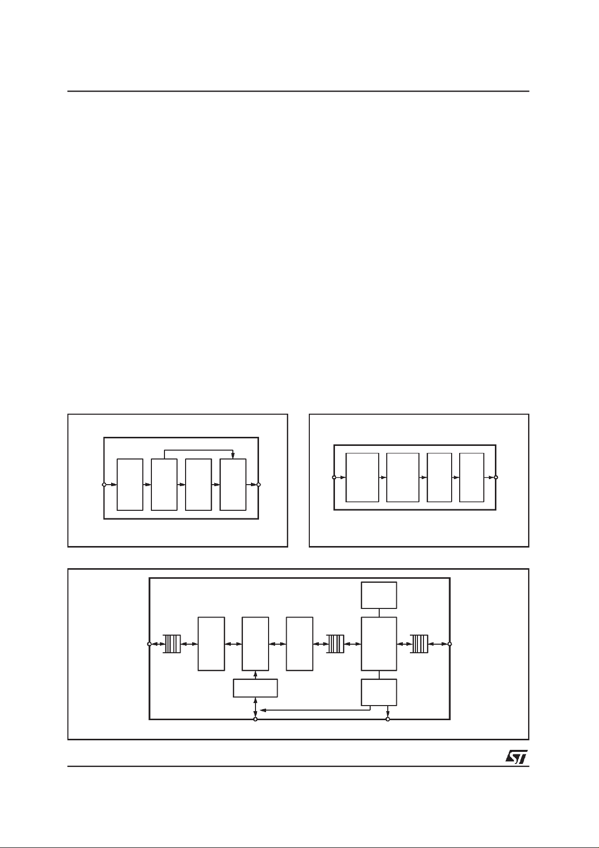
STLC60135 interfaces
Overview
Figure 9. STLC60135interfaces
AFE INTERFACE TO
ADSL LINE (STLC60134)
The STLC60135 is controlled and configured by
an external processor across the processor interface. All programmable coefficients and parameters are loaded throughthis path.
The ADSL initialization is also controlled by this
interface
Two interface types are supported; A generic
asynchronous interface (i.e. PowerPC or any microprocessor interface) and a specific i960 interface. The choice is made by the OBC_TYPEpin.
(0 selects i960 type interface, 1 selects generic
access).
Data andaddressesare multiplexed.
STLC60135 works in 16 bits data access, so ad-
RESET
JTAG
CLOCK
STLC60135
PROCESSOR
INTERFACE
(ATC)
dress bit 0 is not used. Address bit 1 is not multiplexed with data. It has its own pin : BE1
Byte acces are not supported. Access cycle read
or write are always in 16 bits data wide, ie bit address A0 is always zero value. The interrupt request pin to the processor is INTB, and is an
Open Drain output.
DIGITAL
UTOPIA/BITSTREAM INTERFACE
INTERFACE
D98TL368A
Tle STLC60135 supports both little and big endian. The default feature is big endian.
Figure 10. Processor Interface Read cycle i960 mode
ProcessorInterface (ATC)
T
TwTwTwTwTdTrT
a
PCLK
ALE
CSB
RDYB
AD
BE1
WR_RDB
Wait
ADDR DATA
ADD(1)
in
Figure 11. Processor Interface WriteCycle i960 mode
T
TwTwTwTwTdTrT
a
PCLK
ALE
CSB
RDYB
AD
BE1
WR_RDB
Wait
ADDR DATA
ADD(1)
out
a
D98TL324A
a
D98TL325A
ATC samples data
(1): The RDYB output is
in tri-state, except for 2 cycles
STLC60135 samples data
(1): The RDYB output is
in tri-state, except for 2 cycles
continuously
continuously
11/25
Page 12

STLC60135
The processor interface in i960 mode
The i960 mode supportsa synchronousbus interface protocol.
Address and data are multiplexed.The processor
is bus master and the STLC60135 is bus slave.
Synchronous means that all signals are synchronous withthe input clock PCLK pin.
The bus cycles are directly started and drivenby
the processor. Addresses (BE1, AD[2..15]) have
to be present before ATCassertsthe ALE signal.
STLC60135 latches the address on the falling
edge of ALE signal.
The RDYB output is synchronousto PCLK.
A bus cycle consists of an Access cycle (Ta),
Wait cycles (Tw), Data cycle (Td) and Recovery
cycle (Tr).
Processor Interface Pins and Functional Descriptioni960 mode
Name Type Function
AD[0...15] I/O Multiplexed Address/Data bus
BE1 I Address bit 1
ALE I Address Latch Enable
WR_RDB I Accessdirection:Write(1),Read (0)
PCLK I Processor Clock
CSB I Chip Select
RDYB OZ Bus cycle ready indication
INTB O Interrupt
GenericInterface
This interface is suitable for a number of processors using a multiplexedAddress/databus. In this
case, synchronisation of the input signals with
PCLK pin is not necessary.
Figure 12. Generic ProcessorInterface Write TimingCycle
T
alew
ALE
CSB
AD(15-0)
WRB
READY
T
ale2cs
T
avs
T
cs2wr
T
cs2rdy
T
avh
T
wr2d
T
wdvd
T
wrw
T
wr2cs
T
dvh
T
mclk
T
csre
RDB
Figure 13. Generic ProcessorInterface Read Timing Cycle
T
T
alew
ale2Z
ALE
CSB
AD(15-0)
RDB
READY
WRB
12/25
T
ale2cs
T
avs
T
avh
T
wr2d
T
wdvd
T
csrd
T
wrw
T
csrs
T
csre
T
T
T
rdy2wr
rd2cs
T
rdy2dr
dvh
D98TL327
T
mclk
D98TL328
Page 13

STLC60135
Genericprocessor interface Cycle Timing
All AC characteristicsare indicatedfor a 100pF capacitiveload.
Symbol Parameters Min Typ Max Unit
tr & tf Rise & Fall time (10% to 90%) 3 ns
Talew ALE pulse width 12 ns
Tavs Address Valid setup time 10 ns
Tavh Address Valid Hold time 10 ns
Tale2cs ALE to CSB 0 ns
Tale2Z ALE to high Z state of address bus 50 ns
Tcs2rdy CSB to RDYB asserted 60 ns
Tcsre Access Time 900 µs
Tcs2wr CSB to WRB 0 ns
Twr2d WRB to data 15 ns
Trdy2wr RDYB to WRB 0 ns
Tdvs data setup time 10 ns
Tdvh data hold time 1/2Tmclk Tmclk ns
Twr2cs WRB to CSB -10 ns
Tcs2rd CSB to RDB 0 ns
Trdy2rd RDY to RDB 0 ns
Trd2cs RDB to CSB -10 ns
Tmclk Master clock Timing
Figure14.Waveforms
T
alew
ALE
AD(15:0)
T
avs
Generic Processor Interface Pins and Functional Description
Name Type Function
AD[0..15] I/O Multiplexed address / data bus
ALE I Address Latch Enable
RDB I Read cycle indication
WRB I Write cycle indication
CSB I Chip Select
RDYB OZ Buscyclereadyindication
INTB O Interrupt
Digital interfaceATM or serial
Digital Interface for data to the loop before modulation andfrom the loop after demodulation.
Thisinterfacecollectscells (fromthe cellbasedfunction module) or a byte stream (from the deframer).
T
avh
D98TL326
Cells are stored in a fifo, 2 interfac es submodules
can extract data from the fifo. Byte streams are
dumped on the bitstream interface (with no fifo).
3 kinds of interfaceare allowed
UtopiaLevel1
UtopiaLevel2
Bitstreambased on a proprietaryexchange
The interface selection is programmed by writing
the Utopia PHY addressregister.
Only one interface can be enabled in a ST60135
configuration.
Utopia Level 1 supports only one PHY device.
Utopia Level 2 supports multi-PHY devices (See
Utopia Level 2 specifications).
Each bufferprovides storagefor 8 ATM cells (both
directionsfor Fastand Interleavedchannel).
13/25
Page 14

STLC60135
The Utopia Level 2 supports point to multipoint
configurationsby introducingan addressingcapability and by making distinction between polling
and selectinga device.
Figure15.ReceiveInterface
ATMPHY
RxREF*
RxCLAV
PHY
RECEIVE
RxENB*
RxCLK
RxDATA
RxSOC
D98TL330
CELL
RECEIVE
8
Figure16.TransmitInterface
PHY
PHY
TRANSMIT
TxREF*
TxCLAV
TxENB*
TxCLK
TxDATA
TxSOC
8
ATM LAYER
CELL
TRANSMIT
Utopia Level 1 Interface
The ATM forum takes the ATM layer chip as a
reference. It defines the direction from ATM to
physical layer as the Transmit direction. The direction from physical layer to ATM is the Receive
direction. Figures 15 & 16 show the interconnection between ATM and PHY layer devices, the
optional signals are not supported and not
shown.
The Utopia interface transfers one byte in a single clock cycle, as a result cells are transformed
in 53 clockcycles.
Both transmit and receive are synchronized on
clocks generated by the ATM layer chip, and no
specific relationshipbetween receive and transmit
clocks is required.
In this mode, the STLC60135 can only support
one data flow : either interleaved or fast .
Figure17.Timing(Utopia 1 ReceiveInterface)
RxCLK
RxSOC
RxENB
RxDATA
RxCLAV
X H1 H2 P44 P45 P46 P47 P48 X
D98TL369
D98TL370
Pin Description
Name Type Meaning Usage Remark
RxClav O Receive Cell available Signals to the ATM chip that the
STLC60135 has a cell ready for
transfer
RxEnb* I Receive Enable Signals to theSTLC60135 that the
ATM chip will sample and accept
data during next clock cycle
RxClk I Receive Byte Clock Gives the timing signal for the
transfer, generated by ATM layer
chip.
RxData O Receive Data (8bits) ATM cell data, from STLC60135
chip to ATM chip, byte wide. Rx
Data [7] is the MSB.
RxSOC O Receive Start Cell Identifies the cell boundary on
RxData
RxRef * O Reference Clock 8 kHz clock transported over the
network
*Active low signal
14/25
Remains active for the entire cell
transfer
RxData and RxSOC could be tristate when RxEnb* is inactive
(high). Active low signal
Indicate to the ATM layer chip that
RxData contains the first valid byte
of a cell.
Activelow signal
Page 15

STLC60135
When RxEnb is asserted, the STLC60135reads
data from its internal fifo and presents it on
RxData and RxSOC on each low-to-high transi-
tion of RxClk, ie the ATM layer chip samples all
RxData and RxSOC on the rising edge of RxSOC
on the rising edge of RxClk.
Pin Description
Name Type Meaning Usage Remark
TxClav O Transmit Cell available Signals to the ATM chip that the
physical layer chip is ready to
accept a complete cell
TxEnb* I Transmit Enable Signals to the STLC60135 that
TxData and TxSOC arevalid
TxClk I Transmit Byte Clock Gives the timing signal for the
transfer, generated by ATM layer
chip.
TxData I Transmit Data (8bits) ATM cell data, from ATM layer chip
to STLC60135, byte wide. TxData
[7] is the MSB.
TxSOC I Transmit Start of Cell Identifies the cell boundary on
TxData
TxRef * I Reference Clock 8kHz clock from the ATM layer chip
*Active low signal
Remains active for the entire cell
transfer
TxData contains the first validbyte
of the cell.
The STLC60135 samples TxData and TxSOC
signals on the rising edge of TxClk, if TxEnb is
asserted.
RxData, RxSOC, RxClav AC electrical characteristics
TxClk, RxClk, AC electrical characteristics
Symbol Parameters Min Max Unit
Symbol Parameters Min Max Unit
F Clock frequency 1.5 25 MHz
Tc Clock duty cycle 40 60 %
Tj Clock peak to peak jitter 5 %
Trf Clock rise fall time 4 ns
L Load 100 pF
TxData, TxSOC, AC electricalcharacteristics
Symbol Parameters Min Max Unit
T5 Inputset-uptimeto TxClk 10 ns
T6 Hold time to TxClk 1 ns
L Load 100 pF
T7 Input set-up time to
TxClk
T8 Hold time to Tx Clk 1 ns
T9 Signal going low
impedance to RxClk
T10 Signal going High
impedance to RxClk
T11 Signal going low
impedance to RxClk
T12 Signal going High
impedance to RxClk
L Load 100 pF
10 ns
10 ns
0ns
1ns
1ns
Figure18.Timing (Utopia 1 Transmit Interface)
TxCLK
TxSOC
TxENB
TxDATA
TxCLAV
X H1 H2 P44 P45 P46 P47 P48 X
D98TL371
15/25
Page 16

STLC60135
Figure19.TimingSpecification(Utopia 1)
CLOCK
SIGNAL
(at input)
SIGNAL
(highz)
T11 T9 T12 T10
T5,T7
T6,T8
D98TL331
DIGITAL INTERFACE
Utopia Level 2 Interface
The ATM forum takes the ATM layer chip as a
reference. It defines the direction from ATM to
physical layer as the Transmit direction. The direction from physical layer to ATM is the Receive
direction. Figure 20 shows the interconnection
between ATM and PHY layer devices, the optional signals are not supportedand not shown.
The UTOPIA interface transfers one byte in a single clock cycle, as a result cells are transferred in
53 clockcycles.
Both transmit and receive interfacesare synchronized on clocks generated by the ATMlayer chip,
and no specificrelationshipbetween Receive and
Transmit clock is assumed, they must be regarded as mutually asynchronous clocks. Flow
Figure20. Signal at Utopia Level2 Interface
PHY
RECEIVE
control signals are available to match the bandwidth constraints of the physical layer and the
ATM layer. The UTOPIA level 2 supports point to
multipoint configurations by introducing on addressing capability and by making a distinction
between polling and selectinga device:
- the ATM chip polls a specific physical layer chip
by putting its address on the address bus when
the Enb* line is asserted. The addressed physical
layer answers the next cycle via the Clav line reflecting its status at thattime.
- the ATM chip selects a specificphysical layer by
putting its address on the address bus when the
Enb* line is deasserted and asserting the Enb*
line on the next cycle. The addressed physical
layer chip will be the target or source of the next
cell transfer.
ATMPHY
RxADDR 5
RxCLAV 1
RxENB*
RxCLK
RxDATA 8
RxSOC
RxREF*
ATM
RECEIVE
16/25
PHY
TRANSMIT
TxADDR 5
TxCLAV 1
TxENB*
TxCLK
TxDATA 8
TxSOC
TxREF*
D98TL329
ATM
TRANSMIT
Page 17

Utopia Level 2 Signals
The physical chip sends cell data towards the
ATM layerchip.
The ATM layer chip polls the status of the fifo of
the physical layer chip.
The cell exchange proceedslike:
a) The physical layer chip signals the availability
of a cell by asserting RxClav when polled by the
ATM chip.
b) The ATM chips selects a physical layer chip,
then starts the transfer by asserting RxEnb*.
c) If the physical layer chip has data to send, it
puts them on the RxData line the cycle after it
sampled RxEnb* active. It also advances the offset in the cell. If the data transferred is the first
byte of a cell, RxSOC is 1b at the time of the data
transfer, 0b otherwise.
d) The ATM chip accepts the data when they are
available. If RxSOC was 1b during the transfer, it
resets its internal offset pointer to the value 1,
otherwise it advancesthe offset in the cell.
STLC60135
STLC60135 Utopia Level 2 MPHY Operation
Utopia level 2 MPHY operation can be done by
various interface schemes. The STLC60135 supports only the required mode, this mode is referred to as ”Operation with 1 TxClav and 1
RxClav”.
PHY Device Identification
The STLC60135 holds 2 PHY layer Utopia ports,
one is dedicated to the fast data channel, the
other one to the interleaved data channel. The
associated PHY address is specified by the
PHY_ADDR_x fields in the Utopia PHY address
register. Beware that an incorrect address configuration may lead to bus conflicts. A feature is
defined to disable(tri-state) all outputsof the Utopia interface. It is enabled by the TRI_STATE_EN
bit in the Rx_interfacecontrol register.
Pin DescriptionUtopia 2 (ReceiveInterface)
Name Type Meaning Usage Remark
RxClav O Receive Cell available Signals to the ATM chip that the
STLC60135 has a cell ready for
transfer
RxEnb* I Receive Enable Signals to the physical layer that
the ATM chip will sample and
accept data during next clock cycle
RxClk I Receive Byte Clock Gives the timing signal for the
transfer, generated by ATM layer
chip.
RxData O Receive Data (8 bits) ATM cell data, from physical layer
chip to ATM chip, byte wide.
RxSOC O Receive Start Cell Identifies the cell boundary on
RxData
RxAddr I Receive Address(5 bits) Use to select the port that will be
active or polled
RxRef * O Reference Clock 8kHz clocktransportedover the
network
*Active low signal
Remains active for the entire cell
transfer
RxData and RxSOC could be tristate when RxEnb* is inactive
(high)
Indi ca teto theATMlayerchipthat
RxData contains the first validbyte
of a cell.
17/25
Page 18

STLC60135
Pin Description Utopia 2 (Transmitinterface)
Name
TxClav O Transmit Cell
TxEnb* I Transmit Enable Signals to thephysical layer that
TxClk I Transmit Byte Clock Gives the timing signal for the
TxData I Transmit Data (8 bits) ATM cell data, to physical layer
TxSOC I Transmit Start of Cell Identifies the cell boundary on
TxAddr I Transmit Address
TxRef * I Reference Clock 8kHz clock from the ATM layer chip
*Active low signal
BitStreamInterface
The Bitstream interface is a proprietary point to
Type
Meaning Usage Remark
available
(5 bits)
Signals to theATM chip that the
physical layer chip is ready to
accept a cell
TxData and TxSOC are valid
transfer, generated by ATM layer
chip.
chip to ATM chip, byte wide.
TxData
Use to select the port that will be
active or polled
enabled by the TransceiverController. A disabled
cell interfacedoes not dump data on its interface.
point interface. The STLC60135 is the bus master of the interface. The interface is synchronous,
a common clockis used.
Receive SLAP Interface
The interface signals use 2 signaltypes: (refer to
fig. 22)
SLAP (Synchronous Link Access Protocol) Interface
The SLAP interface is a point to point bitstream
interface. The STLC60135 is the bus master of
the interface.
The interface is synchronous, a common clock
(SLAP_CLOCK) is used. The basic idea is illustrated in Figure 20.
The SLAP interface dumps the data of the fast
and interleavedchannels on 2 separatesub interfaces.
The data flow from the SLAP interface must be
- SLR_DATA[1:0]:data pins, a byte is transferred
in 4 cycles of 2 bits. The msb are transmitted first,
odd bitsare asserted on SLR_DATA[1].
- SLR_VAL: indicates the data transfer and the
byte boundary
- SLR_FRAME: indicates the start of a superframe
Notice 2 SLAP interfaces are supported, one for
the fast data flow, the other one for the interleaved data flow.
The logic timingdiagram is shown in figure 23.
Remains active for the entire cell
transfer
Figure21.CommonClockDataTransfer
18/25
SOURCE
RISING
CLOCK
DCKQ
QN
SLAP_CLOCK
FALLING
CLOCK
DCKQ
QN
SINK
D98TL332
Figure22. ReceivePath,SLAPInterface
SLAP_CLOCK
DATA 2
EXTERNAL
COMPONENT
(SLAVE)
VALID
FRAME
MODEM
(MASTER)
D98TL333
Page 19

Figure23.ReceiveSLAPInterfaceTiming
STLC60135
STM_CLOCK
VALID
SLR_DATA(1)
SLR_DATA(0)
0123 8
minimum 8 cycles
UNDEFINED UNDEFINEDFRAME
b7 b5 b3 b1
one byteas 4 times 2 bits
b6 b4 b2 b0
The implementation must guarantee that all active SLR_Valid signals must be separated by at
least 8 clock cycles.
Refer to Figure 23. The SLR_FRAME signals are
asserted when the first pair of bits of a frame are
transferred. For the fast channel a frame is defined as a superframetimebase.
For the interleaved channel the frame is defined
by a timebase period of 4 superframes. Both
timebasesare synchronizedto the data flow.
TransmitSLAP Interface
The Transmit interface uses the following signals
(refer to Figure 24)
- SLT_REQ:byte request
- SLT_FRAME:start of frameindication
Figure24. InterfaceTowardsPHYLayer
CLOCK
SLR_VAL must not repeat
a 8 clock cycle period
D98TL334
in
- SLT_DATA [1:0] data pins, a byte is transferred
2 bits at the time in 4 successive clock cycles.
MSB first, odd bits on SLT_DATA[1]
The logical timing diagram is shown in Figure 25.
The delay between Request and the associated
data byte is defined as 8 cycles.
The SLT_FRAME signals are asserted when the
first pair of bitsof a frame are transferred.For the
fast channel a frame is defined as a superframe
timebase.
For the interleaved channel the frame is defined
by a timebaseperiod of 4 superframes.
Both timebasesare synchronized to the data flow
and guarantee that the frame indication is asserted when the first bits of the first DMT symbol
are transferred.
Figure25.TransmitSLAP InterfaceTiming
Diagram
REQUEST
EXTERNAL
COMPONENT
(SLAVE)
DATA2
FRAME
Figure26.InterfaceTiming
CLOCK
T
s
ALL INPUTS
ALL OUTPUTS
ThT
T
hd
T
d
0891CLOCK
MODEM
(MASTER)
D98TL335
T
per
i
D98TL337
SLT_REQUEST
SLT_DATA(1)
SLT_DATA(0)
11
102
b7 b5 b3 b1
one byte in 4 cycles
b6 b4 b2 b0
UNDEFINEDSLT_FRAME
STM_CLOCK
Request may be repeated after 4
Delay Request-Data equals 8 cycles
repeated each superframe/
S-frame
UNDEFINED
D98TL336
cycles
19/25
Page 20

STLC60135
SLAP INTERFACE, AC ElectricalCharacteristics
Symbol Parameter Test Condition Min. Typ. Max. Unit
Tper Clock Period refer to MCLK ns
Th Clock High 11 ns
Tl Clock Low 11 ns
Ts Setup 3 ns
Thd Hold 2 ns
Td Data Delay 20pF load 3 6 ns
AnalogFront End Control Interface
The Analog Front End Interface is designed to be
connected to the STLC60134 Analog Front End
component.
TransmitInterface
The 16 bit words are multiplexed on 4 AFTXD
output signals. As a result 4 cycles are needed to
transfer 1 word. Refer to table 1 for the bit/pin allocation for the 4 cycles. The first of 4 cycles is
identifiedby the CLWD signal. Refer to Figure 26.
Figure27. TransmittWordTimingDiagram
MCLK
CLWD
AFTXD
AFTXED
Cycle0 Cycle1 Cycle2 Cycle3
GP_OUT
Test0 Test1 Test2 Test3
D98TL320
Figure28. ReceiveWord TimingDiagram
MCLK
CLWD
AFRXD
Cycle0 Cycle1 Cycle2 Cycle3
GP_IN(0)
Test0 Test1 Test2 Test3
D98TL321
The STLC60135 fetches the 16 bit word to be
multiplexed on AFTXD from the Tx Digital FrontEnd module.
Receive Interface
The 16 bit receive word is multiplexed on 4
AFRXD input signals. As a result 4 cycles are
needed to transfer 1 word. Refer to Table 2 for
the bit / pin allocationfor the 4 cycles.The first of
4 cycles is identified by the CLWD must repeat
after 4 MCLK cycles.
Table 1: Transmitted Bits Assigned to Signal /
Time Slot
Cycle 0 Cycle 1 Cycle 2 Cycle 3
AFTXD[0] b0 b4 b8 b12
AFTXD[1] b1 b5 b9 b13
AFTXD[2] b2 b6 b10 b14
AFTXD[3] b3 b7 b11 b15
GP_OUT t0 t1 t2 t3
Table 2: Transmitted Bits Assigned to Signal /
Time Slot
Cycle 0 Cycle 1 Cycle 2 Cycle 3
AFRXD[0] b0 b4 b8 b12
AFRXD[1] b1 b5 b9 b13
AFRXD[2] b2 b6 b10 b14
AFRXD[3] b3 b7 b11 b15
GP_IN t0 t1 t2 t3
Figure29.TransmitInterface
20/25
MCLK
AFTXD
AFTXED
CLWD
Tc
Tv
D98TL322
Figure30. ReceiveInterface
MCLK
Ts
Th
AFRXD
D98TL323
Page 21

STLC60135
Table 3: Master Clock (MCLK) AC ElectricalCharacteristics
Symbol Parameter Test Condition Min. Typ. Max. Unit
F Clock Frequency 35.328 MHz
Tper Clock Period 28.3 ns
Th Clock Duty Cycle 40 60 %
Table 4: AFTXD, AFTXED, CLWD AC Electrical Characteristics
Symbol Parameter Test Condition Min. Typ. Max. Unit
Tv Data Valid Time 0 10 ns
Tc Data Valid Time 0 10 ns
Table 5: AFRXD AC ElectricalCharacteristics
Symbol Parameter Test Condition Min. Typ. Max. Unit
Ts Data setup Time 5 ns
Th Data hold Time 5 ns
Tests, Clock, JTAG Interface
- Mclk: Master Clock (35.328MHz) generated by
VCXO
- ATM receive interface, asynchronousclock generated by Utopia Master
- ATM transmit interface, asynchronous clock
generatedby Utopia Master
- ATC clock (Pclk): external asynchronous clock
(synchronouswith ATC in case of i960 specificinterface)
JTAG TP interface: Standard Test Access Port,
Used with the boundary scan for chip and board
testing.
This JTAG TAP interface consistsin 5 signals:
TDI, TDO, TCK & TMS.
TSRTB: Test Reset, reset the TAP controller.
TRSTB is an activelow signal.
Table 6: BoundaryScan Chain Sequence
Sequence
Number
2 AD_0 B
3 AD_1 B
4 AD_2 B
6 AD_3 B
7 AD_4 B
9 AD_5 B
10 AD_6 B
12 AD_7 B
13 AD_8 B
14 AD_9 B
16 AD_10 B
Mnemonic Pin BS Type
17 AD_11 B
19 AD_12 B
21 PCLK I
23 AD_13 B
24 AD_14 B
25 AD_15 B
27 BE1 I
28 ALE C
30 CSB I
31 WR_RDB I
32 RDYB O
33 OBC_TYPE I
34 INTB O
35 RESETB I
38 U_RxData_0 B
39 U_RxData_1 B
41 U_RxData_2 B
42 U_RxData_3 B
44 U_RxData_4 B
45 U_RxData_5 B
46 VSS
47 U_RxData_6 B
48 U_RxData_7 B
50 U_RxADDR_0 I
51 U_RxADDR_1 I
52 U_RxADDR_2 I
53 U_RxADDR_3 I
55 U_RxADDR_4 I
56 GP_IN_0 i
58 GP_IN_1 I
60 U_RxRefB O
21/25
Page 22

STLC60135
Table 6: (continued)
Sequence
Number
61 U_TxRefB I
63 U_RxCLK
64 U_RxSOC
65 U_RxCLAV
66 U_RxENBB
68 U_TxCLK
69 U_TxSOC
70 U_TxCLAV
71 U_TxENBB
74 U_TxData_7 I
75 U_TxData_6 I
77 U_TxData_5 I
78 U_TxData_4 I
79 U_TxData_3 I
80 U_TxData_2 I
82 U_TxData_1 I
83 U_TxData_0 I
84 U_TxADDR_4 I
85 U_TxADDR_3 I
87 U_TxADDR_2 I
88 U_TxADDR_1 I
89 U_TxADDR_0 I
90 SLR_FRAME_F
92 SLR_FRAME_S
93 SLR_DATA_S_1
94 SLR_DATA_S_0
96 SLR_DATA_S
97 SLR_DATA_F_1
98 SLR_DATA_F_0
99 SLR_VAL_F
100 SLAP_CLOCK
101 SLT_FRAME_F
103 SLT_DATA_F_1
104 SLT_DATA_F_0
105 SLT_DATA_S_1
106 SLT_DATA_S_0
107 SLT_REQ_F
110 SLT_REQ_S
111 SLT_FRAME_S
112 TDI
113 TDO
114 TMS
116 TCK
118 TRSTB
119 TESTSE none
120 GP_OUT O
Mnemonic Pin BS Type
121 PDOWN O
123 AFRXD_0 I
124 AFRXD_1 I
125 AFRXD_2 I
126 AFRXD_3 I
128 CLWD 1 I
129 MCLK 1 C
130 CTRLDATA 1 O
132 AFTXED_0 O
133 AFTXED_0 O
135 AFTXED_0 O
136 AFTXED_0 O
138 IDDq none
139 AFTXD_0 O
140 AFTXD_1 O
142 AFTXD_0 O
143 AFTXD_1 O
Generalpurpose I/O register
2 generalPurpose Register (0x040)
Field Type
GP_IN R [0,1] 2 Sampled level
GP_OUT RW [2] 1 Output level on
Position
bits
Length
Function
on pins GP_IN
pins GP_OUT
bits from 3 to 15are reserved
Reset Initialization
The STLC60135 supports two reset modes:
- A ’hardware’ reset is activated by the RESETB
pin (active low). A hard reset occurswhen a low
input value is detected at the RESETB input.
The low level must be applied for at least 1ms
to guarantee a correct reset operation. All
clocks and power supplies must be stable for
200ns prior to the rising edge of the RESETB
signal.
- ’Soft’ reset activated by the controller write access to a soft reset configuration bit. The reset
process takes less than 10000 MCLK clock cycles.
ELECTRICALSPECIFICATIONS
Generic
The values presented in the following table apply
for all inputs and/or outputs unless specified otherwise. Specifically they are not influenced by the
choicebetween CMOS or TTL levels.
22/25
Page 23

STLC60135
DC ElectricalCharacteristics
(All voltages are referencedto VSS, unless otherwisespecified, positivecurrent is towards the device)
IO Buffers Generic DC Characteristics
Symbol Parameter Test Condition Min. Typ. Max. Unit
I
IN
I
OZ
I
PU Pull up Current VIN =VSS -25 -66 -125 mA
I
PD
R
PU
R
PD
IO Buffers Dynamic DC Characteristics
Important for transient but measured at (near) DC
Symbol Parameter Test Condition Min. Typ. Max. Unit
C
IN Input Capacitance @f = 1MHz 5 pF
dl/dt Current Derivative 8mA driver, slew rate control 23.5 mA/ns
I
peak
C
OUT
Input Leakage Current VIN=VSS,VDDno pull up /
-10 10
µ
pull down
Tristate Leakage Current VIN=VSS,VDDno pull up /
-10 10
µ
pull down
Pull Down Current VIN=V
Pull up Resistance VIN=V
Pull Down Resistance VIN=V
DD
SS
DD
25 66 125 mA
50 K
50 K
8mA driver, no slew rate control 89 -125 mA/ns
Peak Current 8mA driver, slew rate control 85 mA
8mA driver, no slew rate control 100 mA
Output Capacitance (also
@f = 1MHz 7 pF
bidirectional and tristate drivers)
A
A
Ω
Ω
Input / Output CMOS GenericCharacteristics
The values presented in the following table apply for all CMOS inputs and/or outputs unless specified
otherwise.
CMOS IO Buffers Generic Characteristics
Symbol Parameter Test Condition Min. Typ. Max. Unit
V
IL
V
IH
V
HY
Low Level Input Voltage 0.2 x V
High Level Input Voltage 0.8 x V
Schmitt trigger hysteresis slow edge < 1V/ms, only for
DD
0.8 V
DD
V
V
SCHMITx
V
OL
V
OH High Level Output Voltage IOUT = XmA* 0.85 x VDD V
* The reference current is dependent on the exact buffer chosen and is a part of the buffer name. The available values are 2, 4 and 8mA.
Low Level Output Voltage I
= XmA* 0.4 V
OUT
Input/ Output TTL Generic Characteristics
The values presented in the following table apply for all TTL inputs and/or outputs unless specified otherwise
Symbol Parameter Test Condition Min. Typ. Max. Unit
V
IL
V
IH
V
ILHY
V
IHHY
V
HY
V
OL Low Level Output Voltage IOUT = XmA* 0.4 V
V
OH High Level Output Voltage IOUT = XmA* 2.4 V
* The reference current is dependent on the exact buffer chosen and is a part of the buffer name. The available values are 2, 4 and 8mA.
Low Level Input Voltage 0.8 V
High Level Input Voltage 2.0 V
Low Level Threshold, falling slow edge < 1V/ms 0.9 1.35 V
High Level Threshold, rising slow edge < 1V/ms 1.3 1.9 V
Schmitt Trigger Hysteresis slow edge < 1V/ms 0.4 0.7 V
23/25
Page 24

STLC60135
PQFP144 PACKAGE MECHANICAL DATA
DIM.
mm inch
MIN. TYP. MAX. MIN. TYP. MAX.
A 4.07 0.160
A1 0.25 0.010
A2 3.17 3.42 3.67 0.125 0.135 0.144
B 0.22 0.38 0.009 0.015
C 0.13 0.23 0.005 0.009
D 30.95 31.20 31.45 1.219 1.228 1.238
D1 27.90 28.00 28.10 1.098 1.102 1.106
D3 22.75 0.896
e 0.65 0.026
E 30.95 31.20 31.45 1.219 1.228 1.238
E1 27.90 28.00 28.10 1.098 1.102 1.106
E3 22.75 0.896
L 0.65 0.80 0.95 0.026 0.031 0.037
L1 1.60 0.063
K
D
D1
PQFP144
73108
72
36
109
B
144
1
e
0°
37
(min.), 7°(max.)
E3D3E1
E
L1
A
A2
A1
0.10mm
.004
Seating Plane
B
C
L
K
24/25
Page 25

STLC60135
Information furnished is believed to be accurate and reliable. However, STMicroelectronics assumes no responsibility for the consequences
of use of such information nor for any infringement of patents or other rights of third parties which may result from its use. No license is
granted by implication or otherwise under any patent or patent rights of STMicroelectronics. Specification mentioned in this publication are
subject to change without notice. This publication supersedes and replaces all information previously supplied. STMicroelectronics products
are not authorized for use as critical components in life support devices or systems without express written approval of STMicroelectronics.
The ST logo is a trademark of STMicroelectronics
Tosca is trademark of STMicroelectronics
1999 STMicroelectronics and Alcatel Alsthom, Paris – Printed in Italy – All Rights Reserved
STMicroelectronics GROUP OF COMPANIES
Australia - Brazil - China - Finland - France - Germany - Hong Kong - India - Italy - Japan - Malaysia - Malta - Morocco -
Singapore - Spain - Sweden - Switzerland - United Kingdom - U.S.A.
http://www.st.com
25/25
 Loading...