

Page 1
TOSCA INTEGRATEDADSL CMOS
FULLY INTEGRATEDAFEFORADSL
OVERALL 12 BIT RESOLUTION, 1.1MHz
SIGNAL BANDWIDTH
8.8MS/sADC
8.8MS/sDAC
THD: -60dB @FULL SCALE
4-BIT DIGITAL INTERFACE TO/FROM THE
DMT MODEM
1V FULL SCALEINPUT
DIFFERENTIAL ANALOGI/O
ACCURATE CONTINUOUS-TIME CHANNEL
FILTERING
3rd & 4th ORDER TUNABLE CONTINUOUS
TIME LP FILTERS
0.5 WATTAT 3.3V
0.5µm HCMOS5 LA TECHNOLOGY
64 PIN TQFP PACKAGE
DESCRIPTION
STLC60134S is the Analog Front End of the
STMicroelectronics Tosca ADSL chipset and
when coupled with STLC60135 (DTM modem)al-
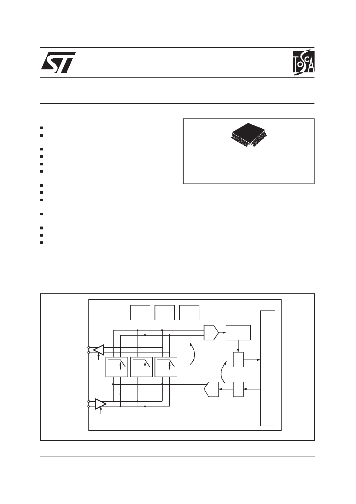
Figure 1. Block Diagram
STLC60134S
ANALOG FRONT-ENDCIRCUIT
TQFP64
ORDERING NUMBER: STLC60134S
lows to get a T1.413Issue 2 compliantsolution.
The STLC60134S analog front end handles 2
transmissionchannels on a balanced 2 wire interconnection; a 16 to 640Kbit/s upstream channel
and a 1.536 to 8.192Mbit/sdownstreamchannel.
A 256 carrier DMT coding (frequency spacing
4.3125kHz) transforms the downstream channel
to a 1MHz bandwidth analog signal (tones 32-
255) and the upstream channel (tones 8-31) to a
100kHzbandwidthsignal on the line.
This asymmetricaldata transmission system uses
high resolution, high speed analog to digital and
digital to analog conversion and high order analog filtering to reduce the echo and noise in both
August 1999
TXP
TXN
RXP(0:1)
RXN(0:1)
G=-15...0dB
step=1dB
+
+
-
AGCtx
G=0..31dB
step=1dB
+
+
-
AGCrx
1.1MHz
HC2
R-MOS-C
TUNING
1.1MHz
HC1
I/V-REF
138KHz
SC2
XTAL-DRIVER
VCXO
DAC
ANALOG
LOOP
ADC
DAC MUX
ERROR
CORRECTION
MUX
DIGITAL
LOOP
12 bits 4 bits
13 bits
4 bits
D99TL453
DIGITAL
IF
1/22
Page 2

STLC60134S
the ATU-C/ATU-R receivers and transmitters.External low noise driver and input stage used with
STLC60134Sguarantee low noise performances.
The STLC60134S chip can be used at ATU-C
and ATU-R ends (behaviour set by LTNT pin).
The selection consists mainly of a filter interchange between the RX and TX path. The filters
(with a programmablecutoff frequency) use automatic Continuous Time Tuning to avoid time varying phase characteristicwhich can be of dramatic
consequencefor DMT modem. It requiresfew external components, uses a 3.3V supply (a separate 3.0V supply of the digital part is possible)
and is packaged in a 64-pin TQFP in order to reduce PCB area.
The Receiver (RX) part
The DMT signal coming from the line to the
STLC60134S is first filtered by the two following
external filters:
POTSHP filter: Attenuation of speech and POTS
Channel filter:
signalling
Attenuation of echo signal to
improve RX dynamic
An analog multiplexer allows the selection between two input ports which can be used to select
an attenuated(0, 10dB for ex.) version of the signal in case of short loop or large echo. The signal is amplified by a low noise gain stage (031dB) then low-pass filtered to avoid anti-aliasing
and to ease further digital processing by removing unwantedhigh frequencyout-of-bandnoise.
A 12-bit A/D converter samples the data at
8.832MS/s (or 4.416MS/s in alternative mode),
transforms the signal into a digital representation
and sends it to the DMT signal processor via the
digital interface.
The Transmitter(TX) part
The 12-bit data words at 8.832MS/s (or
4.416MS/s) coming from the DMT signal processor through the digital interface are transformed
by D/A converterinto a analog signal.
This signal is then filtered to decrease DMT sidelobes level and meet the ANSI transmitter spectral response but also to reduce the out-of-band
noise (which can be echoedto the RX path)to an
acceptable level. The pre-driver buffers the signal
for the external line driver and in case of short
loop provide attenuation(-15...0dB).
The VCXO part
The VCXO is divided in a XTAL driver and a auxiliary 8 bits DAC for timing recovery.
The XTAL driver is able to operateat 35.328MHz
and provides an amplitude regulation mechanism
to avoid temperature / supply / technology de-
pendent frequencypulling.
The DAC which is driven by the CTRLIN pin provides a current output with 8-bit resolution and
can be used to tune the XTAL frequency with the
help of external components. A time constant between DAC input and VCXO output can be introduced (via the CTLIN interface) and programmed
with the help of an external capacitor (on VCOC
pin).
See chapter ’VCXO’ for the external circuit related to the VCXO
.
The Digital Interfacepart
The digital part of the STLC60134S can be divided in 3 sections:
The data interface converts the multiplexed
data from/to the DMT signal processor into
valid representation for the TX DAC and RX
ADC. It performs also the error correction
mechanism needed at the (redundant) ADC
output.
The control interface allows the board processor to configure the STLC60134S paths
(RX/TX gains, filter band, ...) or settings (OSR,
vcodac enable,digital / analog loopback,...).
The test interface to enable digital (Full Scan,
nandtree, loop backs, functional,...) or analog
(TIN, TOUT assignation) tests to be performed.
DMT Signal
A DMT signal is basically the sum of N independently QAM modulated signals, each carried
over a distinct carrier. The frequency separation
of each carrier is 4.3125kHz with a total number
of 256carriers (ANSI). For N large, the signal can
be modelledby a gaussianprocess with a certain
amplitude probability density function. Since the
maximum amplitude is expected to arise very
rarely, we decide to clip the signal and to tradeoff the resulting SNR loss against AD/DA dynamic. A clipping factor (Vpeak/Vrms= ”crest factor”) of 5 will be used resulting in a maximum
SNR of 75dB.
ADSLDMTsignalsarenominallysentat-40dBm/Hz
±3dB (-3.65dBm/carrier) with a maximal power of
100mW for down link transmitterand 15.7mWfor
uplink transmitter.
DMT symbols are transmitted without ’windowing’ causing sin (x)/x like sidelobes. For spectral
response shaping, the 1st sidelobe level is assumed to be 13dB under the carrier level with
an attenuationof -20dB/dec.
The minimum SNR + D needed for DMT carrier
⋅
demodulation is about (3
N + 20) dB with a
minimum of 38dB were N is the constellation size
of a carrier(in bits).
2/22
Page 3

STLC60134S
Maximum/ minimumsignal levels
The following table gives the transmitted and received signal levels for both ATU-R and ATU-C
sides. All the levels are referred to the line volt-
mit power and line impedance signal amplitudes
can differ from thesevalues.
The referenceline impedance for all power calculationsis 100Ω.
ages (i.e. after hybrid and transformers in TX direction, before hybrid and transformer in RX direction).
Note that signal amplitudes shown below are for
illustration purpose and depending on the trans-
Table 1. Target Signal Levels
Parameter ATU - C ATU - R
Max level 839 mVpdif 15.8 Vpdif 3.95 Vpdif 3.4 Vpdif
Max RMS level 168 mVrms 3.16 Vrms 791 mVrms 671mVrms
Min level 54 mVpdif 3.95 Vpdif 42 mVpdif 839 mVpdif
Min RMS level 11 mVrms 791 mVrms 8 mVrms 168mVrms
Table 2. Total Signal Level
Parameter ATU - C ATU - R
Max level for receiver 4 Vpdif (Long line) 4.2 Vpdif (Short line)
(on the line).
RX TX RX TX
(on the line).
RX TX RX TX
PACKAGE
The STLC60134S is packaged in a 64-pin TQFP
package (body size 10x10mm,pitch 0.5mm).
Figure 2. Pin Connection
TX1
TX0
NU3
NU2
NU1
NU0
CTRLIN
DVSS1
CLKM
CLNIB
CLWD
RX3
RX2
RX1
RX0
TX3
TX2DVDD2
62
63
64
1
2
3
4
5
6
7
8
9
10
12
13
14
15
16DVDD1
17 18 19 20 21
PDOWN
AVSS1
DVSS2
61
LTNT
RESETN
XTALO
XTALI
AVDD1
RES
VCXO
AVDD2
IVCO
IREF
AVSS2
60
59 58 57 56 5455 53 52 51 50 49
22 23 24 25 26
GP0
RES
VRAP
AVSS3
271128 29 30 31 32
VREF
VRAN
AVDD3
AVDD4
NC0
AVSS6
NC1
RXIP1
TXP
RXIN1
48
47
46
45
44
43
42
41
40
39
38
37
36
35
34
33
TXN
RXIP0
RXIN0
GC1
GC0
VCOC
GP2
AVDD6
AVDD5
RES
RES
AGND
RES
RES
AVSS5
AVSS4
GP1
D98TL355mod
3/22
Page 4

STLC60134S
Table 3. Pin Functions.
N. Name Function PCB connection Supply
ANALOGINTERFACE
24 VRAP positive voltage reference ADC Decoupling network AVDD3
25 VREF ground reference ADC Decoupling network AVDD3
26 VRAN negative voltage reference ADC Decoupling network AVDD3
31 TXP pre driver output Line driver input AVDD4
32 TXN pre driver output Linedriver input AVDD4
38 AGND virtual analog ground (AVDD/2 = 1.65V) Decoupling network AVDD5
44 VCOC VCODAC time constant capacitor VCODAC cap. AVDD5
45 GC0 External gain control output LSB AVDD5
46 GC1 External gain control output MSB AVDD5
47 RXN0 analog receive negative input Gain0 Echo filter output AVDD5
48 RXP0 analog receive positive input Gain 0 Echo filter output AVDD5
49 RXN1 analog receive negative input Gain1 (most sensitive input) Echo filter output AVDD5
50 RXP1 analog receive positive input Gain 1 (most sensitive input) Echo filter output AVDD5
53 IREF current reference TX DAC/DACE Decoupling network AVDD2
55 IVCO current reference VCO DAC VCO bias network AVDD1
56 VCXO VXCO control current VCXO filter AVDD1
59 XTALI XTAL oscillator input pin Crystal + varicap AVDD1
60 XTALO XTAL oscillator output pin Crystal + varicap AVDD1
DIGITAL INTERFACE
1 TX1 digital transmit input, parallel data DVDD2
2 TX0 digital transmit input, parallel data DVDD2
7 CTRLIN serial data input (settings) Async Interface DVDD2
9 CLKM master clock output, f = 35.328MHz Load = CL<30pF DVDD2
10 CLNIB nibbleclock output,f = 17.664MHz(OSR= 2) or ground(OSR = 4) Load = CL<30pF DVDD2
11 CLWD word clock output, f = 8.832/4.416MHz Load =CL<30pF DVDD2
12 RX3 digital receive output, parallel data Load =CL<30pF DVDD2
13 RX2 digital receive output, parallel data Load =CL<30pF DVDD2
14 RX1 digital receive output, parallel data Load =CL<30pF DVDD2
15 RX0 digital receive output, parallel data Load =CL<30pF DVDD2
18 PDOWN power down select, ”1” = power down Power down input DVDD2
19 LTNT ATU-R / ATU-C select pin
20 RESETN reset pin (active low) RC- reset DVDD2
22 GP0 General purpose output 0 (on AVDD 1) Echo filter output AVDD
33 GP1 General purpose output 1 (on AVDD 1) Echo filter output AVDD
43 GP2 General purpose output 2 (on AVDD 1) Echo filter output AVDD
63 TX3 digital transmit input, parallel data Load =CL<30pF DVDD2
64 TX2 digital transmit input, parallel data Load =CL<30pF DVDD2
21 RES RESERVED Must be connected
36,
37,39,
40, 57
RES
mode MSB
SUPPLYVOLTAGES
8 DVSS1 DVSS
16 DVDD1 Digital I/O supplyvoltage DVDD
17 DVDD2 digital internal supply voltage DVDD
23 AVSS3 AVSS
27 AVDD3 ADC supplyvoltage AVDD
1
, ATU-R = 0 /ATU-C = 1 / test
RESERVED
VDD in ATU-C mode DVDD2
to DVSS (input)
Must be connected
to AVSS (input)
4/22
Page 5

STLC60134S
Table 3. Pin Functions
(continued)
28 AVDD4 TX pre - drivers supply AVDD
34 AVSS4 AVSS
35 AVSS5 AVSS
41 AVDD5 CT filter supply AVDD
42 AVDD6 LNA supply AVDD
51 AVSS6 AVSS
52 AVSS2 AVSS
54 AVDD2 DAC and support circuit AVDD
58 AVDD1 XTAL oscillator supply voltage AVDD
61 AVSS1 AVSS
62 DVSS2 DVSS
SPARES
3 NU3 Not used inputs DVSS
4 NU2 Not used inputs DVSS
5 NU1 Not used inputs DVSS
6 NU0 Not used inputs DVSS
29 NC0
30 NC1
1
LT ↔ AUT-C; NT ↔ ATU-R
Figure 3. Grounding and DecouplingNetworks.
VRAP pin VRAN pin
10µF 100nF 10µF 100nF
10µF 100nF
10µF
VREF pin
ANALOG
VDD
IREF pin VCOC pin
ATU-C END: BLOCK DIAGRAM
The transformer at ATU-C side has 1:2 ratio. The
termination resistors are 12.5Ω in case of 100Ω
lines.
The hybrid bridge resistors should be < 2.5kΩ for
low-noise.
An HP filter must be used on the TX path to re-
4.7µ
H
L1
10µF 100nF
10µF100nF
10µF100nF
AVDD (each pin
have its own capacitor)
100nF
AGND pin
must
D98TL356
duce DMT sidelobes and out of band noise influence on the receiver. On the RX path, a LP filter
must be used in order to reduce the echo signal
level and to avoid saturation of the input stage of
the receiver.
The POTS filter is used in both directions to reduce crosstalk between STLC60134S signals
and POTS speech and signalling.
5/22
Page 6

STLC60134S
Figure 4. ATU-C ENDBlock Diagram.
POTS
LINE
Zo=100
2:1
HP POTS FILTER
RXT1 RXT2
RR
2R 2R
LP
POTS FILTER
12.512.5 LPF
GRX
RXP(0:1)
RXN(0:1)
0..31dB
LNA
35.328MHz
XTRAL
DRIVER
LP138KHz
SC2
12-bit A/D
CONVERTER
MASTER CLOCK
35.328MHz
NIBBLES 17.664MHz
WORD 8.832/4.416MHz
RXn
8.832MS/s
4.416MS/s
4
CTRLIN
LTNT=1
RESETN
TO
STLC60135
GTX
LINE
DRIVER
TXP
HPF
TXN
-15..0dB
PD
ATU-R END: BLOCK DIAGRAM
The ATU-R side block diagram is equal to the
ATU-C side block diagram with the following differences:
- Thetransformerratio is 1:1
- Terminationresistors are 50Ω for 100Ω lines.
An LP filter may be used on the TX path to re-
Figure 5. ATU-R END Block Diagram.
POTS
LINE
Zo=100
1:1
HP POTS FILTER
RXT1 RXT2
RR
5050 HPF
2R 2R
LP
POTSFILTER
GRX
RXP(0:1)
RXN(0:1)
VCXOUT
VCODAC
0..31dB
LNA
LP 1.1MHz
HC2
12-bit D/A
CONVERTER
4
D98TL357mod
TXn
8.832MS/s
4.416MS/s
duce DMT sidelobes and out of band noise influence on the receiver. On the RX path, a HP filter
must be used in order to reduce the echo signal
level and to avoid saturation of the input stage of
the receiver.
The POTS filter is used in both directions to reduce crosstalk between ADSL signals and POTS
speech and signalling. Low pass POTS filter can
be verysimple for Lite - ADSLapplication
35.328
MHz
MASTER CLOCK
XTAL
DRIVER
LP 1.1MHz
HC2
12- bitA/D
CONVERTER
35.328MHz
NIBBLES17.664MHz
WORD 8.832/4.416MHz
RXn
8.832MS/s
4.416MS/s
4
CTRLIN
LTNT=0
RESETN
TO
STLC60135
6/22
GTX
LINE
DRIVER
LPF
TXP
TXN
-15..0dB
PD
LP 138KHz
SC2
12-bit D/A
CONVERTER
4
D98TL358mod
TXn
8.832MS/s
4.416MS/s
Page 7
STLC60134S
RX PATH
Speech filter
An external bi-directional LC filter for up and
downstream POTS service splits the speech signal from the ADSL signal to the POTS circuits on
ATU-C.
The ADSL analog front end integrated circuit
does not contain any circuitry for the POTS service but it guarantees that bandwidth is not disturbed by spurious signals from the ADSL-spectrum.
Channel Filters
The external analog circuits provide partial echo
cancellation by an analog filtering of the receive
signal for both ATU-R (Reception of downstream
channel) and ATU-C (Reception of upstream
channel). This is feasible because the upstream
and the downstream data can be modulated on
separatecarriers (FDM).
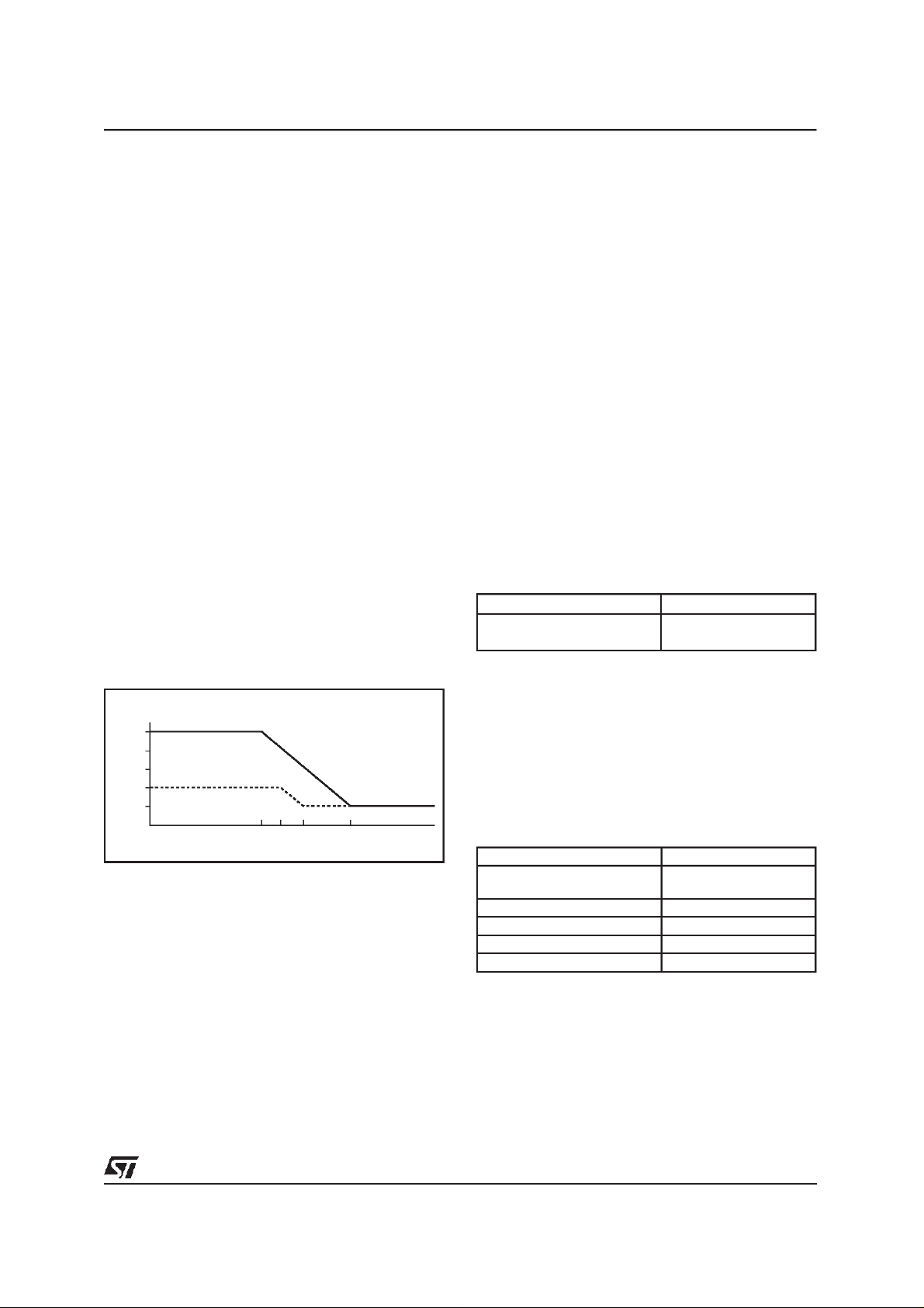
Line Noise Model
The power spectral density of the crosstalk noise
sources as described in ANSI document is given
in the figure below (no HDB3 interferer signals).
Also given in dotted line, is the noise model used
in this document to specify the sensivity requirements which are strongerthan the original ones.
Figure 6. CrosstalkPSD.
dBm/Hz
-100
-110
-120
-130
-140
D98TL359
79.5 138 250 795 kHz
the frequency band of interest. The maximum
noise density within the pass band can exceed
the average valueas follows:
ATU-R RX path (max AGCsetting):
<100nVHz
<31nVHz
-1/2
@ 138kHz
-1/2
for 250kHz< f
ATU-C RX path (max AGCsetting):
<100nVHz
-1/2
for 34.5kHz< f <138kHz
RX-PATHNOISE AT MINIMUM GAIN
At the minimum AGC the total average thermal
noise of the analog RX-path at the ADC input
should be lower than the ADC quantisationnoise.
The maximumnoise density within the pass band
can exceed the average value as follows:
ATU-R RX path (min AGCsetting):
<500nVHz
-1/2
@ 138kHz< f
ATU-C RX path (min AGCsetting):
<1.5µVHz
-1/2
@ 34.5kHz < f < 138kHz
These noise specifications correspond with 10bit
resolutionofthe complete RX-path.
Table 4. RX Common-mode Voltage
Description Value/Unit
Common mode signal V
at RXIN1 and RXIN2:
CM
1.6V < V
CM
<1.7V
AGC of RX path
The AGC gain in the RX-path is controlled
through a 5-bits digital code.
Four inputs are provided for RX input and the selection is made with the RXMUX bits of the
CTRLIN interface. This can be used to make
lower gain paths in case of high input signal.
Table 5. AGC Characteristics.
Signal to Noise Performance
RX- PATH SENSITIVITY AT MAXIMUM GAIN
The RX path sensitivity at the maximal RX-AGC
of the ATU-R receiver is defined at -140dBm/Hz
(for 100Ω ref) on the line. This figure corresponds
to the equivalent input noise of 31nVHz
-1/2
seen
on the line.
The sensitivity at the maximal RX - gain of the
ATU-C receiver is defined at -130dBm/Hz (for
100Ω ref) on the line. The figure corresponds to
the equivalent input noise of 100nVHz
-1/2
seen
on the line.
Both noise figures include the noise of the hybrid.
It is the equivalent average thermal noise over
Description Value/Unit
Input referred noise
(max. gain)
Max. input level 1Vpd
Max. output level 1Vpd
Gain range 0to 31dB withstep = 1dB
Gain and step accuracy
20nVHz
±
-1/2
0.3dB
RX Filters
The combination of the external filter (an LC ladder filter typically) with the integrated lowpass filter must provide:
- echo reduction to improve dynamicrange
- DMT sidelobe and out of band(anti-aliasing)
attenuation.
- Anti alias filter (60dB rejection @ image freq.)
7/22
Page 8

STLC60134S
ATU-R RX Filters
The integratedfilter havethe following characteristics:
Table 6. IntegratedHC Filter Characteristics
Description Value/Unit
Input referred noise 100nVHz
Max. input level 1Vpd
Max. output level 1Vpd
Type 3rd order butterworth
Frequency band 1.104MHz (0%setting, see below)
Frequency tuning -43.75%->+0%
Max. in-band ripple 1dB
Matlab Model
Default cut off frequency @ -3dB
Actual cut off @ -3dB
HC Freq. selection register
[B, A] = butter (3, w0, ’s’)
F0 = 1560KHz
w0 = 2 * pi * F0/((20 + n)/16)
n = -4,..,3
see (AFE settings ,Table 22)
-1/2
Table 7. Phase Characteristic
Description Value/Unit
Total RX filter group delay < 50µs @ 138kHz < f < 1.104MHz
Total RX filtergroup delay distortion < 15µs @ 138kHz < f < 1.104MHz
Figure 7. HC Filter Mask for ATU-R RX and ATU-C TX
AMPLITUTDE
0dB
+/-1dB
5dB 36dB 50dB
30 1104 2208 7728 16560 kHz
Note: The total ATU_RRX path (including ADC) group delay distortion is 16µs (i.e. = 15µs+1µs of ADC)
D98TL360
ATU-C RX filter
This filter is the sameas the one used forATU-R TX.
Linearity of RX
Linearity of the RX analog path is defined by the IM3 product of two sinusoidal signals with frequencies
f1 and f2 and each with 0.5Vpd amplitude (total ≤ 1Vpd) at the output of the RX - AGC amplifier (i.e: before the ADC) for the case of minimalAGC setting.
The following tables 8 and 9 list the RX path intermodulation distortion (as S/IM3 ratio) in downstream
and upstreambandwidth.
Table 8. Linearity of ATU-R RX
f1 (0.5Vpd)
f2 (0.5Vpd)
S/IM3 (AGC = 0dB) 59.5dB @ 100kHz
8/22
300kHz
200kHz
53.5dB @ 400kHz
43.5dB @ 700kHz
42.5dB @ 800kHz
500kHz
400kHz
59.5dB @ 300kHz
48.0dB @ 600kHz
700kHz
600kHz
48.0dB @ 500kHz
42.5dB @ 800kHz
Page 9

Table 9. Linearity of ATU-C RX
STLC60134S
f1 (0.5Vpd)
f2 (0.5Vpd)
S/IM3 (AGC = 20 dB) 2f2 - f1
2f1 - f2
80kHz
70kHz
56.5dB @ 60kHz
56.5dB @ 90kHz
Table 10. RX Filter to A/D Interface
RX filter to A/D maximal level: 1Vpd = full scale of A/D
Table 11. A/D Convertors (A pipeline architectureis used for A/Dconvertors).
Numbers of bits: 12bits
Minimum resolution of the A/D convertor 11bits
Linearity error of the A/D convertor <1LSB (out of 12bits)
Full scale input range: 1 Vpdif ±5%
Sampling rate: 8.832MHz (or 4.416MHz in OSR = 2 mode)
Maximum attenuation at 1.1MHz: <0.5dB without in-band ripple
Maximum group delay: <3µs
Maximum group delay distortion: <1µs
Power Supply Rejection
The noise on the power supplies for the RX path must be lowerthanthe following:
<50mVrmsin bandwhite noisefor any AVDD.
In this case, PSR (power supply rejection)of STLC60134SRX path is lower than -43dB.
TX PATH
TransmitterSpectralResponse
The two figures below show the ANSI spectral response mask for ATU-C and ATU-R transmitters
Figure 8. ATU-C TX spectralresponse mask
dBm/Hz
-40
-64
-90
+/-3dB
24dB 50dB
30 1104 2208 11040 KHz
D98TL361
Figure 9. ATU-R TX spectralresponse mask
dBm/Hz
-40
-64
-88
+/-3dB
24dB 48dB
30 138 181 224 KHz
D98TL362
9/22
Page 10

STLC60134S
Table 12. AGC of TX Path (from filter output to TXP and TXN).
0.3dB
-1/2
capacitive
< 50nVHz
<138kΩ
-1/2
@f>250k
-1/2
@ 34.5K < f
> 500
Ω
< 30pF
Ω
Output noise 25mVHz
Input level (nominal) 1Vpd
Output level nominal, full-scale 1.5Vpd
Maximum Output Load > 500Ω; <10pF
AGC range: -15dB...dB
AGC step: 1dB
Gain and step accuracy
±
Minimum code (0000) stands for AGC = -15dB and maximum (1111 - MSB left) for AGC = 0dB (See Tx
setting, Table22).
TX Pre-driverCapability
The pre-driver drives an external line power amplifierwhich transmits the required power to the line.
Table 13. TX Pre-driver
TX drive level to the external line driver for max. AGC setting 1.5 Vpdif
External line driver input impedance: resistive
Pre-driver characteristics:
closed loop gain: -15dB...0dBwith step = 1dB
ooutput impedance:
output offset voltage (0dB) < 10mV
input noise voltage (0dB) < 20nVHz
output common mode voltage: 1.6V < Vcm < 1.7V
TX Filter
The TX filters act not only to suppress the DMT sidebands but also as smoothingfilters on the D/A convertor’s output to suppress the image spectrum. For this reason they must be realized in a continuous
time approach.
ATU-R TX Filter
The purpose of this filter is to remove out-of-bandnoise of the ATU-R TX path echoed to the ATU-R RX
path. In order to meet the transmitter spectral response, an additional filtering must be (digitally) performed. Theintegrated filter has the following characteristics:
Table 14. IntegratedSC Filter Characteristics
Description Value/Unit
Input referred noise 100nVHz
Max. input level 1Vpd
Max. output level 1Vpd
Type 4th order chebytchef
Frequency band 138kHz (0%settingseebelow)
Frequency tuning -25%->+25%
Max. in-band ripple 1dB
Matlab Model
Default cut-off frequency @ -3dB
Actual cut-off @ -3dB
SC Freq. selection register
[B,A] = cheby1 (4,0.5,W0,’s’) {ripple= 0.5}
F0 = 151.8kHz
W0 = 2*pi*F0/((17+n)/16)
n = -4,..,3
see (AFE settings, Table 22)
-1/2
10/22
Page 11

STLC60134S
Table 15. Phase characteristics
Description Value/Unit
Total TX filter group delay <50µs @ 34.5kHz < f < 138kHz
Total TX filter group delaydistortion <20µs @ 34.5kHz < f < 138kHz
Note: The total ATU-RTX path (including DAC) group delay distortion is 16µs (i.e. = 15µs+1µs of DAC)
Figure 10. SC Filter Mask for ATU-CRXand ATU-R TX
AMPLITUTDE
0dB
+/-1dB
20dB
30 138 250 KHz
D98TL363
Table 16. D/A Convertor (A currentsteering architectureis used).
Description Value/Unit
Numbers of bits: 12bits
Minimum resolution of the D/A convertors 11bits
Linearity error of the A/D convertor <1LSB (out of 12bits)
Full scale input range: 1 Vpdif±5%
Sampling rate: 8.832MHz (or 4.416MHz in compatible mode)
Maximum group delay: <3µs
Maximum group delay distortion: <1µs
Linearity of ATU-C TX
Linearity of the TX is defined by the IM3 productof two sinusoidal signals with frequenciesf1 and f2 and
eachwith0.5Vpdamplitude(total≤ 1Vpd)atthe outputof thepre-driverforthe caseof atotalAGC= 0dB.
Table 17. Linearityof ATU-CTX
f1 (0.5Vpd)
f2 (0.5Vpd)
S/IM3 (AGC = 0dB) 59.5dB @ 100kHz
300kHz
200kHz
53.5dB @ 400kHz
43.5dB @ 700kHz
42.5dB @ 800kHz
500kHz
400kHz
59.5dB @ 300kHz
48.0dB @ 600kHz
700kHz
600kHz
48.0dB @ 500kHz
42.5dB @ 800kHz
11/22
Page 12

STLC60134S
Linearity of ATU-R TX
Table 18. Linearityof ATU-RTX
f1 (0.5Vpd)
f2 (0.5Vpd)
S/IM3 (AGC = 0 dB)
80kHz
70kHz
59.5dB (@ 60KHz, 90KHz)
TX IDLE CHANNEL NOISE
ATU-C TX idle channel noise
The idle channel noise specificationscorrespond with 11bit resolution of the complete TX-path. ATU-C
TX idle channeloutput noise on TX.
Table 19. ATU-C TX idle channel noise
For max AGC setting (0dB)
In-band noise
Out-of-band noise
For min AGC setting (=-15dB)
In-band noise 80nVHz
500nVHz
500nVHz
-1/2
-1/2
-1/2
@ 138kHz -1.104MHz
@ 34.5kHz -138kHz
@ 138kHz -1.104MHz
ATU-R TX idle channel noise
ATU-R TX idle channel outputnoise on TXP, TXN
Table 20. ATU-R TX idle channel noise
For max AGC setting (0dB)
In-band noise
Out-of-band noise
For min AGC setting (=-15dB)
In-band noise 500nVHz
1.6µVHz
1.6µVHz
150nVHz
-1/2
-1/2
-1/2
-1/2
@ 34.5kHz -138kHz
@ 138kHz
@ 250kHz -1.104MHz
@ 34kHz -138kHz
Power Supply Rejection
The noise on the power supplies for the TX-path must be lower than the following:
< 50mVrmsin-bandwhite noise for AVDD.
< 15mVrmsin-bandwhitenoiseforPre-driverAVDD.
VCXO
A voltage controlled crystal oscillator driver is integrated in STLC60134S. The nominal frequency is
35.328MHz.The quartz crystalis connectedbetweenthe pins XTALIand XTALO.
The principle of the VCXOcontrol is shownin figure11.
The information coming from the digital processor via the CTRLIN path is used to drive an 8-bit DAC
which generates a control current. This current is externally converted and filtered to generate the required control voltage (range:-15V to 0.5V)for the varicap. The VCXO circuit characteristicsare given in
Table 21.
12/22
Page 13

STLC60134S
Table 21. VCXO circuit Characteristics
Symbol Parameter Min. Nominal Max. Note
f
abs
f
range
I
O
I
i
N.B: frequency tuningrangeis proportional to the crystal dynamic capacitance Cm.
Figure 11. Principleof VCXO control
Absolute frequency accuracy -15ppm 35.328MHz +15ppm
Frequency Tuning Range
50ppm
±
VCXO Output Current 100µA Rref = 16.5k
AVDD = 3.3V
Reference Input Current 100µA 1mA AVDD = 3.3V
AVDD
S
C
÷AVDD/2
VCOCX
AVDD/22
Ω
CTRLIN
8 bits
DAC
(seeCTRLIN table)
1M
Ω
±30%
Filtered VCXO
Clk35
IVCO R
VCXOUT
XTALO
XTALI
REF
Ii
C
P
AVDD
IO=Ii
t Rt
C
D98TL364mod
AGND
-15V
The tuning mustbe monotonicwith 8-bit resolutionwith the worst-casetuning step of <2ppm/LSB(8-bit).
s
The time constant of the tuning must be variable from 5s to 10s through an external capacitor C
(R =
1MΩ ±30%). This determines the speed of the VCXO in normal operation (slow speed in ”show time”)
with filtered VCXO.For faster tracking, the previous filter is not used and the speeddepends on CtRt.
13/22
Page 14

STLC60134S
DIGITAL INTERFACE
ControlInterface
The digital setting codes for the STLC60134S configuration are sent over a serial line (CTRLIN) using
the word clock (CLWD).
The data burst is composed of 16 bits from whichthe first bit is used as start bit (’0’), the three LSBs being used to identify the data contained in the 12 remaining bits. Test related data are overruled by the
normal settingsif the TEST pin is low.
Table 22. Control InterfaceBit Mapping
M
S
B
b9b8b7b6b5b4b3b2b1b
b
b
b
b
b
b
1
1
4
5
0 x 0 0 0 External Gain Control GC1 (init = 0)
0 x 0 0 0 External Gain Control GC0 (init = 0)
0 0 0 0 0 Rx input selected = RXIN0, RXIP0 (init)
0 1 0 0 0 Rx input selected = RXIN1, RXIP1
0 00000 000AGCRXGain setting 0dB (init)
0 00001 000AGCRXGain setting 1dB
0 x x x x x 0 0 0 AGC RX Gain setting XdB
0 11111 000AGCRXGain setting 31dB
0 0 0 0 0 0 Normal mode Filter selection see LTNT pin (init)
0 0 1 0 0 0 In ATU-C conf, force HC2 for RX path, TX grounded
0 1 0 0 0 0 In ATU-C conf, force HC1 for RX path
0 1 1 0 0 0 Normal mode Filter selection see LTNT pin
b
b
1
1
4
5
0 0 0 0 0 0 0 1 TransmitTX - AGC setting -15dB (init)
0 0 0 0 1 0 0 1 TransmitTX - AGC setting -14dB
0 x x x x 0 0 1 TransmitTX - AGC setting (X - 15) dB
0 1 1 1 1 0 0 1 TransmitTX - AGC setting 0dB
0 0000 001Notused (init)
0 0000 001Notused (init)
0 0000 001Notused (init)
0 0000 001Notused (init)
0 x x x 0 0 1 General Purpose Output (GPO)setting (init = 000)
b
b
1
1
4
5
0 0 0 1 0 NormalMode (Digital path) (init)
0 1 0 1 0 Digital Loopback (digitalTX to digitalRX - DAC not used)
0 0 0 1 0 Normal Mode (Analog path)
0 1 0 1 0 Analog loopback (RXi to TXi - ADC not used)
0 0 0 1 0 VCO DAC disabled
0 1 0 1 0 VCO DAC enabled (init)
0 0 0 1 0 HC filter enabled (init)
0 1 0 1 0 HC filter enabled
1) After initialization, this bit has to be cleared (0) to make the device properly operate.
1
1
2
3
b
b
1
1
2
3
b
b
1
1
2
3
1
1
0
1
b9b8b7b6b5b4b3b2b1b
b
b
1
1
0
1
b9b8b7b6b5b4b3b2b1b
b
b
1
1
0
1
L
S
B
0
0 TX SETTINGS
0 AFE SETTINGS
RX SETTINGS
1)
(init)
14/22
Page 15

STLC60134S
Table 22. Control InterfaceBit Mapping (continued)
b9b8b7b6b5b4b3b2b1b
b
b
b
b
b
b
1
1
4
5
0 0 0 1 0 OSR set to 4 (init)
0 1 0 1 0 OSR set to 2
0 1 1 1 0 1 0 SC freq. selection: Fc = 138kHz (init) (*)
0 0 1 1 0 1 0 SC freq. selection: Fc ~ 110kHz (*)
0 1 0 1 0 1 0 SC freq. selection: Fc ~ 170kHz (*)
0 1 0 0 0 1 0 HC freq. selection: Fc = 1.104MHz (init)(*)
0 0 1 1 0 1 0 HC freq. selection: Fc ~ 768kHz (*)
0 0 0 1 0 VCXO output NOT filtered (”show-time”) (init)
0 1 0 1 0 VCXO output filtered
b
b
1
1
4
5
000000000 011VCODACCURRENT value @ MINIMUM
0 x x x x x x x x 0 1 1 VCO DAC CURRENT value @ X
011111111 011VCODACCURRENT value @ MAXIMUM
b
b
1
1
4
5
0 0 1 0 0 TXD Active (init)
0 1 1 0 0 TXD in powerdown
0 0 1 0 0 N.U. (init)
0 1 1 0 0 N.U.
0 0 1 0 0 ADC Active (init)
0 1 1 0 0 ADC in powerdown
0 0 1 0 0 HFC2 Active (init)
0 1 1 0 0 HFC2 in powerdown
0 0 1 0 0 HFC1 Active (init)
0 1 1 0 0 HFC1 in powerdown
0 0 1 0 0 SCF2 Active (init)
0 1 1 0 0 SCF2 in powerdown
0 0 1 0 0 SCF1 Active (init)
0 1 1 0 0 SCF1 in powerdown
0 0 1 0 0 LNA Active (init)
0 1 1 0 0 LNA inpowerdown
0 0 1 0 0 DAC Active (init)
0 1 1 0 0 DAC in powerdown
0 0 1 0 0 DACE Active (init)
0 1 1 0 0 DACE in powerdown
0 0 1 0 0 VCODAC Active (init)
0 1 1 0 0 VCODAC in powerdown
0 0 1 0 0 XTAL Active (init)
0 1 1 0 0 XTAL in powerdown
b
b
1
1
5
4
0 x x x x x x x x x x x x 1 0 1 RESERVED
0 x x x x x x x x x x x x 1 1 0 RESERVED
0 x x x x x x x x x x x x 1 1 1 RESERVED
(*) For each filter,8 possible frequency values (see table 6 and table 14). Notation is 2’s complementrange from -4 = 100b +3 = 011b.
Fc is the frequencyband (-1dB)
1
1
2
3
b
b
1
1
2
3
b
b
1
1
2
3
b
b
1
1
3
2
1
1
0
1
b9b8b7b6b5b4b3b2b1b
b
b
1
1
0
1
b9b8b7b6b5b4b3b2b1b
b
b
1
1
0
1
b
b
1
1
b9b8b7b6b5b4b3b2b1b
1
0
0 AFE SETTINGS
0 VCO DAC VALUE SETTINGS
0 POWER DOWN ANALOG BLOCK SETTINGS
0 RESERVED
15/22
Page 16

STLC60134S
ControlInterface Timing
The wordclock (CLWD) is usedto sampleat negativegoingedge the control information.The startbit b15
is transmittedfirst followedby bitsb[14:0]andat least16stopbitsneed to be providedto validatethe data.
Figure 12. Control Interface.
CLWD
CTRLIN
START
BIT
D98TL365
DATA
ID.
>=16 STOP BITS=HIGH
Data set-up and hold time versus falling edge CLWD must be greater than 10nsec.
Receive / Transmit Interface
RECEIVE/ TRANSMITPROTOCOL
The digital interfaceis based on 4 x 8.832MHz(35.328MHz) data lines in the following manner:
If OSR = 2 (OSR bit set to 1) is selected, CLKNIBis used as nibble clock (17.664MHz,disabled in normal
mode),and all the RXi, TXi, CLKWDperiodsare twiceas longas in normalmode. This ensuresa compatibilitywithlowerspeedproducts.
TX Signal Dynamic
The dynamic of data signal for both TX DACs is 12 bits extractedfrom the available signed 16 bit representationcomingfromthedigitalprocessor.
The maximalpositive number is 2
14
-1, the most negativenumber is -214, the 3 LSBsare filled with ’0’.
Any signal exceedingthese limits is clamped to the maximumvalue.
Table 23.
BIT MAP/NIBBLE N0 N1 N2 N3
TXD0
TXD1
TXD2 not used data bit 3 data bit 7 data SIGN
TXD3 d0 = data bit 0 (LSB) data bit 4 data bit 8 data SIGN
not used data bit 1 data bit 5 data bit 9
not used data bit 2 data bit 6 data bit 10
Table 24. TX bit map
N3 N2 N1 N0
sign sign d10 d9 d8 d7 d6 d5 d4 d3 d2 d1 d0 n.u. n.u. n.u.
The two sign bits must be identical.
16/22
Page 17

STLC60134S
RX Signal Dynamic
The dynamic of the signal from the ADC is limited to 13bits. Those bits are converted to a signed (2’s
complement)representation with a maximal positive number of 2
The 2 LSBs are filled with ’0’.
Table 25.
BIT MAP/NIBBLE N0 N1 N2 N3
RXD0 0 data bit 2 data bit 6 data bit 10
RXD1
RXD2
RXD3
d0 = data bit 0 (LSB) data bit 4 data bit 8 data SIGN
0 data bit 3 data bit 7 data bit 11
data bit 1 data bit 5 data bit 9 data SIGN
Table 26. RX bit map
N3 N2 N1 N0
sign sign d11 d10 d9 d8 d7 d6 d5 d4 d3 d2 d1 d0 0 0
The two sign bits must be identical.
Figure 13. TX/ RX Digital Interface Timing
14
-1 and a most negative number -214.
CLKM
35.328MHz
CLWD
8.832MHz
TXDx/RXDx
N0 N1 N2 N3
OSR=4
CLKNIB
17.664MHz
CLWD
4.416MHz
TXDx/RXDx
N0 N1 N2 N3
D98TL366
OSR=2
Receive / Transmit interfacetiming
The interface is a triple (RX, TX) nibble - serial interface running at 8.8MHz sampling (normal mode).
The data are represented in 16bits format, and transferred in groups of 4 bits (nibbles). The LSBs are
transferred first. The STLC60134S generates a nibble clock (CLKM master clock in normal mode,
CLKNIBin OSR = 2 mode) and word signalsshared by the three interfaces.
Data is transmitted on the rising edge of the master clock (CLKM/CLKNIB) and sampled on the falling
edge of CLKM/CLKNIB. This holds for the data stream from STLC60134S and from the digital processor.
Data, CLWD setup and hold times are 5ns with reference to thefalling edge of CLKM/CLKNIB.
(notfloating).
17/22
Page 18

STLC60134S
Data is transmittedon the rising edge of the master clock (CLKM/CLKNIB) and sampledon the low going
edgeof CLKM/CLKNIB.Thisholdsforthe datastreamfromSTLC60134Sand from thedigitalprocessor.
Data,CLWDsetupandholdtimesare5nswithreferencetothefallingedgeofCLKM/CLKNIB.(notfloating).
POWERDOWN
When pin Pdown = ”1”, the chip is set in power down mode. As the Pdown signal is synchronouslysampled, minimum duration is 2 periods of the 35MHz clock. In this mode all analog functional blocks are
deactivatedexcept: preamplifiers (TX), clock circuits for output clock CLKM. P
tal part of the chip. Anyway, after a Pdown transition, the digital part status,is updated after 3 clockperiods (worst case)
The chip is activatedwhenP
down
= ”0”.
In power down mode the following conditionshold:
- Outputvoltagesat TXP/TXN= AGND
- Preamplifieris on with maximumgain setting (0dB), (digitalgainsettingcoefficientsareoverruled)
- TheXTALoutputclockonpin CLKMkeepsrunning.
- Alldigital setting are retained.
- Digitaloutput on pins RXDx don’t care (not floating).
In power-down mode the powerconsumptionis 100mW.
Followingexternal conditions are added:
- Clockpin CLW is running.
- CTRLINsignals can still be allowed.
- AGNDremainsat AVDD/2(circuitis poweredup)
- Inputsignal at TXDx inputs are not strobed.
The Pdown signal controls asynchronouslythe power-downof each analog module:
- Aftera few µs the analog channel is functional
- Afterabout 100ms the analog channel delivers full performance
will not affectthe digi-
down
RESET FUNCTION
The reset function is implied when the RESETN pin is at a low voltage input level. In this condition,the
reset functioncan be easilyused for power up reset conditions.
Detailed Description
During reset: (resetis asynchronous,tenths of ns are enough to put the IC in reset)
Allclockoutputsaredeactivatedandput tological”1” (exceptforthe XTAL andmasterclockCLKM)
After reset:(4 clock periods after reset transition,as worst case)
- OSR= 4
- Allanaloggains(RX,TX)aresettominimumvalue
- Nominalfilterfrequencybands(138kH z ,1.104Hz)
- LNAinput = ”11” (max. attenuation)
- VCOdac disabled
- Dependingof the LTNT pin value the following configurationis chosen:
’0’ (ATU-R)
RX: LNA -> HC2 -> ADC
TX: DAC -> SC2 -> TX
’1’ (ATU-C)
RX: LNA -> SC2 -> ADC
TX: DAC -> HC2 -> TX
18/22
Page 19

STLC60134S
Digital outputs are placed in don’tcare condition (non-floating).
N.B.
If a Xtal oscillator is used, the RESET must be released at last 10µs after power-on, to ensure a
correct duty cycle for the clk35clock signal.
ELECTRICAL RATINGS AND CHARACTERISTICS
Table 27. AbsoluteMaximumRatings
Symbol Parameter Min Max Unit
V
V
T
T
I
LU
I
AVDD
I
AVDD
I
DVDD
I
DVDD
DD
in
stg
L
Any VDD Supply Voltage, related to substrate - 0.5 5 V
Voltage at any input pin -0.5 VDD+0.5 V
Storage Temperature -40 125 °C
Lead Temperature (10 second soldering) 300 °C
Latch - up current @80°C 100 mA
Analog Supply Current @ 3.6V - normal operation 165 mA
Analog Supply Current @ 3.6V - power down 30 mA
Analog Supply Current @ 3.6V - normal operation 56 mA
Analog Supply Current @ 3.6V - power down 50 mA
Table 28. ThermalData
Symbol Parameter Value Unit
R
th j-amb Thermal and Junction ambient 50 °C/W
Table 29. OperatingConditions
(Unlessspecified, the characteristic limits of ’Static Characteristics’ in this document apply over an T
-40 to 80 °C; VDD within the range 3 to 3.6V ref. to substrate.
Symbol Parameter Min Max Unit
AVDD AVDD Supply Voltage,related to substrate 3.0 3.6 V
DVDD DVDD Supply Voltage, related to substrate 2.7 3.6 V
V
in/Vout
P
d
T
amb
T
j Junction Temperature -40 110 °C
Voltage at any input and output pin 0 V
DD
Power Dissipation 0.4 0.6 W
Ambient Temperature -40 80 °C
op =
V
19/22
Page 20

STLC60134S
STATIC CHARACTERISTICS
Table 30. Digital Inputs
Schmitt-triggerinputs: TXi, CTRLIN, PDOWN,LTNT, RESETN, TEST
Symbol Parameter Test Condition Min. Typ. Max. Unit
V
IL
V
IH
V
H
C
imp
Table 31. Digital Outputs
Hard Driven Outputs: RXi
Symbol Parameter Test Condition Min. Typ. Max. Unit
V
OL
V
OH
C
load
Low Level Input Voltage 0.3⋅ DVDD V
High Level Input Voltage 0.7⋅ DVDD V
Hysteresis 1.0 1.3 V
Input Capacitance 3 pF
Low Level Output Voltage I
High Level Output Voltage I
= -4mA 0.15⋅DVDD V
out
= 4mA 0.85⋅ DVDD V
out
Load Capacitance 30 pF
Clock DriverOutput: CLKM, CLNIB, CLKWD
Symbol Parameter Test Condition Min. Typ. Max. Unit
V
OL
V
OH
C
load
Low Level Output Voltage I
High Level Output Voltage I
Load Capacitance 30 pF
DC Duty Cycle 45 55 %
= -4mA 0.15⋅ DVDD V
out
= 4mA 0.85⋅ DVDD V
out
20/22
Page 21

STLC60134S
DIM.
mm inch
MIN. TYP. MAX. MIN. TYP. MAX.
A 1.60 0.063
A1 0.05 0.15 0.002 0.006
A2 1.35 1.40 1.45 0.053 0.055 0.057
B 0.18 0.23 0.28 0.007 0.009 0.011
C 0.12 0.16 0.20 0.0047 0.0063 0.0079
D 12.00 0.472
D1 10.00
0.394
D3 7.50 0.295
e 0.50 0.0197
E 12.00 0.472
E1 10.00
0.394
E3 7.50 0.295
L 0.40 0.60 0.75 0.0157 0.0236 0.0295
L1 1.00 0.0393
K 0°(min.),7°(max.)
OUTLINE AND
MECHANICAL DATA
TQFP64
D
D1
A1
TQFP64
3348
16
32
17
E3D3E1
0.10mm
Seating Plane
E
L1
L
K
49
B
64
1
e
A
A2
B
C
21/22
Page 22

STLC60134S
Information furnished is believed to be accurate and reliable. However, STMicroelectronics assumes no responsibility for the consequences
of use of such information nor for any infringement of patents or other rights of third parties which may result from its use. No license is
granted by implication or otherwise under any patent or patent rights of STMicroelectronics. Specification mentioned in this publication are
subject to change without notice. This publication supersedes and replaces all information previously supplied. STMicroelectronics products
are not authorized for use as critical components in life support devices or systems without express written approval of STMicroelectronics.
The ST logo is a trademark of STMicroelectronics
Tosca is trademark of STMicroelectronics
1999 STMicroelectronics and Alcatel Alsthom, Paris – Printed in Italy – All Rights Reserved
STMicroelectronics GROUP OF COMPANIES
Australia - Brazil - China- Finland - France - Germany - Hong Kong - India - Italy - Japan - Malaysia - Malta - Morocco-
Singapore - Spain - Sweden - Switzerland - UnitedKingdom - U.S.A.
http://www.st.com
22/22
 Loading...