

Page 1

STLC60133
XDSL LINE DRIVER
PRELIMINARY DATA
■
LOW NOISE : 4nV/
■
HIGH PEAK OUTPUT CURRENT: 500 mA
■
HIGH SPEED
Hz
– 140MHz Gain Bandwidth
– 30MHz Gain Flatness
– 400 V/us Slew Rate
■
LOW POWER OPERATION
– ±5V to ±15V Voltage Supply
– 12.5 mA/Amp (typ) Supply current
– Power reduced Current
■
LOW SINGLE TONE DISTORTION
■
THERMAL AND OVERLO AD PROTECTION
■
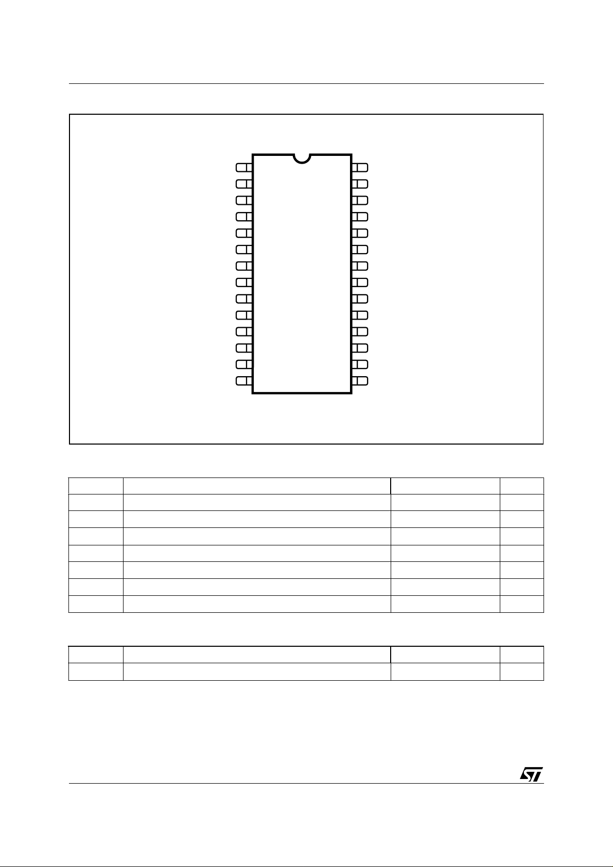
HTSSOP28 PACKAGE
■
-40 TO +85°C OPERATING RANGE
DESCRIPTION
The STLC60133 is a dual amplifier featuring a high
slew rate and a large bandwidth optimized for XDSL
applications. The dev ice is avai lable in a HTSSOP 28
pin package (4x9 mm) with an exposed leadframe.
Thanks to its small pack age thi s l ine driv er is sui table
for high density ADSL line card.
HTSSOP28
ORDERING NUMBER: STLC60133
Temperature Range: -40°C to +85°C
Two digital pins (PWDN0 and PWDN1) allow the driver to work in full performance mode, in low-power
mode or two intermediate bias states.
The low-power mode biases the output stage in or der
to provide a low impedance at the amplifier outputs
for back termination.
The STLC60133 is designed optimizing bandwidth
and distortion perfor mances . For p roper devic e operating it is necessary to work with a gain level greater
than 15.6dB.
Typical differential gain is normally +27dB, while typical common mode gain is 15.6dB
Figure 1. BLOCK DIAGRAM
-V
+V
S
S
Op1
IN1N
IN1P
PWDN0
PWDN1
BIAS
DGND
IN2N
IN2P
October 2001
This is preliminary information on a new product now in development. Details are subject to change without notice.
LOGIC
-
+
-
+
Op2
OUT1
TH DETCT.
OUT2
D00TL462A
1/9
Page 2
STLC60133
PIN CONNECTION
RES
N.C.
N.C.
IN2P
IN2N
OUT2
+V
S
+V
S
OUT1 DGND
IN1N N.C.
2
3
4
5
6
7
8
9
10
IN1P
N.C
N.C. N.C.
12
13
28
27
26
25
24
23
22
21
20
19
18
17
16
RES1
N.C.
N.C.
N.C.
PWDN1
BIAS
-V
S
-V
S
PWDN011
N.C.
1514N.C. N.C.
D00TL463A
ABSOLUTE MAXIMUM RATINGS
Symbol Parameter Value Unit
V
CC
V
SS
V
id
V
T
op
T
stg
T
Positive Supply voltage (note1) +16.5 V
Negative Supply voltage (note1) -16.5 V
Differential Input Voltage (note2) ±5 V
Common mode Input Voltage ±1 V
i
Operating Free Air Temperature Range -40 to +85 °C
Storage temperature -65 to +150 °C
Junction temperature 150 °C
j
THERMAL DATA
Symbol Parameter Value Unit
R
thj-amb
Thermal resistance junction to ambient (note 3) 29 °C/W
2/9
Page 3
STLC60133
OPERATING RANGE
Symbol Parameter Value Unit
T
op
V
CC
V
SS
V
DGND
V
icm
Notes
1) All voltag es values , except differential voltage , are with re spect to netw ork ground term i nal .
2) Differential volt ages are non-inverting in put terminal with resp ect to the inverting inp ut termina l
3) Specification is for device on a 4 layer board within 10 square inches of oz. copper at +85°C and 200m/s air velocity. With 0m/s air velocity
the parameter incre ases up to 33° C/ W
.
PIN DESCRIPTION
2, 3, 12, 13, 14,
15, 16, 17, 19,
25, 26, 27
21, 22 -Vs Negative Supply Voltage
Operating Temperature Range -40 to 85 °C
Positive Supply voltage (note1) +5 to +15 V
Negative Supply voltage (note1) -5 to -15 V
Digital Ground level VSS+5<V
DGND<VCC
Common Mode Input Voltage Range ±1 V
N° Pin Description
NC Not Connected
4 IN2P Non Inverting Input of Op. Amplifier 2
5 IN2N Inverting Input of Op. Amplifier 2
6 OUT2 Ouput of Op. Amplifier 2
7, 8 +Vs Positive Supply Voltage
9 OUT1 Ouput of Op. Amplifier 1
10 IN1N Inverting Input of Op. Amplifier 1
11 IN1P Non Inverting Input of Op. Amplifier 1
14 PWDN1 Power Down 1 logic input
18 PWDN0 Power Down 0 logic input
23 BIAS Bias Control pin
1, 28 RES To be left not connected
-5 V
Power Down Management
The STLC60133 provides several quiescent bias levels from full performance, to reduced bias (in three steps
through PWDN0/1 pins) or to full OFF operation (through BIAS pin). According to the different XDSL application
(both site CO and CPE), different bias levels can be chosen maintaining good MTPR performances. In the following table are shown the bias levels versus the PWDN values.
PWDN1 PWDN0 Bias Level
1 1 100%
1 0 60%
0 1 40%
0 0 25% (low Zout but not OFF)
X X Full OFF (High Zout via 250uA pulled out of BIAS pin)
3/9
Page 4

STLC60133
The bias level is programmed by the TTL logic level applied to the PWDN pins. The DGND pin is the logic
ground reference for the PWDN pins. For normal operation the BIAS pin shall be left open.
The BIAS control pin can be used to adjust the internal biasing and thus the quiescent current. By pulling out a
current of 0
However, considering the internal parameter spread to full shutdown the STLC60133 is recommended to pull
down a 250
plifier shutdown. To partially reduce the internal biasing also the PWDN pins can be used.
Figure 2. Logi c dri v e of bias pin for comp lete A m pl i fier S hutdown.
µ
A to 200µA, the quiescent current can be adjusted from 100% (full ON) to a full OFF condition.
µ
A current from the BIAS pin. In the following figure is shown an implementation of a complete am-
3.3V
R1 = 47KΩ for ± 12V
R1 = 22KΩ for ± 6V
R2
50KΩ
R1
D01TL492
BIAS
STLC60133
THERMAL SHUTDOWN
A thermal protection is embedded in the STLC60133. In case of thermal overload the device is shut down at
160°C and returns to normal operation when the temperature becomes lower than 145°C.
During the thermal shutdown the voltage at the BIAS pin goes to the DGND rail; when the device returns to the
normal operation the voltage at the BIAS pin goes to the positive rai l. In thi s condi tion the BIA S pin can be used
as thermal overload indicator.
MAXIMUM POWER DISSIPATION
Maximum Junction Temperature allowed for proper device operation is Tj = 140°C. A Typical Thermal Resistance Junction to ambient of 29°C/W can be obtai ned mounting the devi ce on a 4 layer board whithin 10 square
inches of copper and having the exposed pad contacting a proper copper area . It shall be noted that the exposed pad of the device is electrically connected to the V
negative supply.
SS
Figure 3. Shutdown and alarm circuit
4/9
V
CC
200µA
PWDN0 PWDN1
V
CC
BIAS BIAS
1/4 HCF40109B
+5V
ST
STLC60133
10KΩ
SHUT
DOWN
BIAS
ALARM
V
EE
OR
D01TL491
V
BIAS=VCC
BIAS
-1.5V
1MΩ10KΩ
100KΩ
OR 0-200µA
+5V
10KΩ
ALARM
MIN β 350
Page 5

STLC60133
ELECTRICAL CHARACTERISTCS
Test Conditions: (VCC = ±12V , Tamb = 0 to 70°C , Single amplifier in normal condition (PWDN0 = 1, PWDN1 = 1),
unless otherwise specified). The limits listed below are guaranted in the above temperature range (0-70°C) by
specific testing at different temperature or by product characterisation.
TRANSMISSION PATH
Symbol Parameter Test Condition Min. Typ. Max. Unit
SR Slew Rate G = 6, Vout = 2Vpp 400 V/us
GBW Gain Bandwidth G = 6, Vout = 2Vpp, f = 5MHz 90 140 MHz
THD Single ended Distortion G = 6, f = 1MHz, Vout = 12Vpp,
DTHD
Differential THD
(2)
Rl = 16.5Ω
Rl = 100Ω
G = 6, f = 1MHz, Vout = 24Vpp,
Rl = 33Ω
Rl = 100Ω
-40
-45
-50
-55
-47
-52
dBc
dBc
IMD Single ended IMD G = 6, Vout = 3Vp each tone,
f = 500KHz, ∆f = 10KHz
DIMD
Differential IMD
(2)
Rl = 16.5Ω
Rl = 100Ω
G = 6, Vout = 6Vp each tone,
f = 500KHz, ∆f = 10KHz
Rl = 33Ω
Rl = 100Ω
-54
-60
-66
-72
-70
-75
dBc
dBc
IB Input Biasing 5 µA
OZ Output Impedance PWDN0 = PWDN1 = 0; f = 1MHz 2 Ω
VN Voltage Noise (RTI) f = 30KHz 4 10
nV/
Hz
IOV Input Offset Voltage 6mV
ICMR Input Common Mode Voltage
f = 1 MHz -1 +1 V
Range
CMRR Common Mode Rejection Ratio f = 1 MHz, Vin = 100mV 40 dB
OVS Output Voltage Swing Single ended, Rl = 100Ω, G = 6 -10.8 +10.8 V
LOC Linear Output Current Single ended, Rl = 10Ω, G = 6 400 600 mA
SCC
Short Circuit Current
QC Quiescent Current PWDN1, PWDN0 = 1,1
(1)
Single ended 1000 1400 mA
PWDN1, PWDN0 = 1,0
PWDN1, PWDN0 = 0,1
PWDN1, PWDN0 = 0,0
12
8
5
4
16.2
10.7
7.5
5.3
mA/Amp
SC Shutdown Current 250µA out of Bias pin 1.5 2.0 mA/Amp
PSRR Power Supply Rejection ratio f = 500kHz, V = 100mV 30 dB
BIASV Bias Pin Voltage 10 10.5 V
DCG DC Gain 80 dB
Notes: 1. The output stage of the STLC60133 is designed for maximum load current capability. As a result, shorting the output to common
can cause the STLC60133 to source or sink 1.4A.
2. Guar ant eed by produc t characterization.
5/9
Page 6

STLC60133
ELECTRICAL CHARACTERISTICS
Test conditions (V
unless otherwise specified.)
= ±6V, T
CC
The limits listed below are guaranted in the above temperature range by (0-70°C)
= 0 to 70°C ,Single amplifier in normal condition (PWDN0 = 1, PWDN1 = 1),
amb
specific testing at different temperature or by product characterisation.
TRANSMISSION PATH
Symbol Parameter Test Condition Min. Typ. Max. Unit
SR Slew Rate G = 6, Vout = 2Vpp 400 V/us
GBW Gain Bandwidth G = 6, Vout = 2Vpp, f = 5MHz 90 140 MHz
THD Single Ended Distortion G = 6, f = 1MHz, Vout = 6Vpp,
Rl = 25Ω
Rl = 100Ω
(2)
(2)
G = 6, f = 1MHz, Vout = 12Vpp,
Rl = 25Ω
Rl = 100Ω
f = 500KHz, ∆f = 10KHz
Rl = 25Ω
Rl = 100Ω
G = 6, Vout = 3Vp each tone,
f = 500KHz, ∆f = 10KHz
Rl = 25Ω
Rl = 100Ω
DTHD
IMD Single Ended IMD G = 6, Vout = 1.5Vp each tone,
DIMD
Differential THD
Differential IMD
IB Input Biasing 5 µA
-40
-45
-50
-55
-65
-70
-77
-82
-46
-51
-76
-81
dBc
dBc
dBc
dBc
VN Voltage Noise (RTI) f = 30KHz 4 10
IOV Input Offset Voltage 6mV
ICMR Input Common Mode Voltage
Range
CMRR Common Mode Rejection Ratio f = 1 MHz, Vin = 100mV 40 dB
OVS Output Voltage Swing Single ended, Rl = 100Ω,
LOC Linear Output Current Single ended, Rl = 10Ω,
SCC
PSRR Power Supply Rejection ratio f = 500kHz, V = 100mV 30 40 dB
BIASV Bias Pin Voltage 4 4.5 V
DCG DC Gain 80 dB
Notes: 1. The output stage of the STLC60133 is designed for maximum load current capability. As a result, shorting the output to common
Short Circuit Current
QC Quiescent Current PWDN1, PWDN0 = 1,1
SC Shutdown Current 250µ A out of Bias pin 1.5 2.0 mA/Amp
can cause the STLC60133 to source or sink 1.4A.
2. Guar ant eed by produc t characterization.
(1)
f = 1 MHz -1 +1 V
-5 +5 V
G = 6
G = 6
Single ended, 1000 1400 mA
PWDN1, PWDN0 = 1,0
PWDN1, PWDN0 = 0,1
PWDN1, PWDN0 = 0,0
300 420 mA
10
3.5
13.7
7
5
9
6.5
4.5
nV/
Hz
mA/Amp
6/9
Page 7

STLC60133
DIGITAL INTERFACE (PWDN0, PWDN1, Vcc = ±12 V or ±6 V)
Symbol Parameter Test Condition Min. Typ. Max. Unit
V
Input low voltage 0 0 .8 V
il
V
Input high voltage 2.2 5.5 V
ih
THERMAL PROTECTION
Symbol Parameter Test Condition Min. Typ. Max. Unit
T
T
Thermal shut down threshold 160 °C
hsd
Thermal detector histeresys 15 °C
hist
Figure 4. Sin gl e e nded Test Circui t G = 6
VIN V
200Ω 1200Ω
-
+
D00TL464
OUT
R
L
+V
S
10µF0.1µF
10µF0.1µF
-V
S
Figure 5. Differential Test Circuit G = 6
10µF
+V
S
0.1µF
200Ω
V
IN
200Ω
+
-
1200Ω
1200Ω
-
+
0.1µF
-V
S
10µF
+V
R
L
-V
D00TL465A
OUT
OUT
7/9
Page 8

STLC60133
DIM.
MIN. TYP. MAX. MIN. TYP. MAX.
A 1.2 0.0
A1 0.15 0.006
A2 0.8 1.0 1.05 0.031 0.039 0.041
b 0.19 0.3 0.007 0.012
c 0.09 0.2 0.003 0.008
D (*) 9.6 9.7 9.8 0.377 0.382 0.385
D1
E 6.2 6.4 6.6 0.244 0.252 0.260
E1 (*) 4.3 4.4 4.5 0.169 0.173 0.177
E2 3.0
e 0.65 0.026
L 0.45 0.6 0.75 0.018 0.024 0.029
L1 1.0 0.039
k 0˚ (min), 8˚ (max)
aaa 0.1 0.004
(*) Dimensions D and E1 does not include mold flash
or protusions. Mold flash or protusions shall not
exceed 0.15mm per side.
mm inch
5.5
0.216
0.118
OUTLINE AND
MECH ANICAL DATA
HTSSOP28
(Exposed Pad)
8/9
A
A2
be
Caaa
D
D1
11 4
28 15
A1 c
EE2
SEATING
PLANE
C
HTSSO28M
E1
0.25mm
0.10inch
GAUGE PLANE
k
L
L1
Page 9

STLC60133
Information furnished is believed to be accurate and reliable. However, STMicroelectronics assumes no responsibility for the consequences
of use of such information nor for any infringement of patents or other rights of third parties which may result from its use. No license is granted
by implic ation or otherwise un der any pat ent or pat ent rights of STMicroelectronics. Spec i fications mentioned in this publication are subject
to change without notice. This publication supersedes and replaces all information previously supplied. STMicroelectronics produ ct s are not
authorized for use as cri t i cal compone nts in life support device s or systems without express written approval of STMi croelectr o nics.
The ST logo is a registered trademark of STMicroelectronics
2001 STMi croelectronics - All Ri ghts Reserved
Australi a - Brazil - Chin a - Finland - Franc e - Germany - Hong Kong - India - Ital y - Japan - Malaysi a - M al ta - Morocco - Sin gapore - S pai n
STMicroelectronics GROUP OF COMPANIES
- Sweden - Sw itzerlan d - United Kingdom - U.S.A.
http://www.s t. com
9/9
 Loading...