

Page 1
STLC5466
64 CHANNEL-MULTI HDLC WITH
N X 64KB/S SWITCHING MATRIX ASSOCIATED
PRELIMINARY DATA
■
64 TX HDLCs with broadcasting capability and/
or CSMA/CR function with automatic restart in
case of Tx frame abort
■
64 RX HDLCs including Address
Recognition
■
16 Command/Indicate Channels (4 or 6-bit
primitiv e )
■
16 Monitor Channels processed in accordance
with GCI or V*
■
256 x 256 Switching Matrix without blocking
and with Time Slot Sequence Integrity and
loopback per bidirectional connection
■
DMA Controller for 64 Tx Channels and 64 Rx
Channels
■
HDLCs AND DMA CONTROLLER ARE
CAPABLE OF HANDLING A MIX OF
LAPD,LAPB, SS7, CAS AND
PROPRIETARY SIGN AL L IN G S
■
External shared memory access
between DMA Controller and Micro
processor
■
SINGLE MEMORY SHARED BETWEEN
n x MULTI-HDLCs AND SINGLE MICRO
PROCESSOR ALLOWS TO HANDLE n x 64
CHANNELS
■
Bus Arbitration
■
Interface for various 8,16 or 32 bit
Microprocessors with fetch memory
to accelerate the exchanges
between Microprocessor and
SHARED MEMORY
■
SDRAM Controller allows to inter
face up to 16 Megabytes of
Synchronous Dynamic RAM
■
Interrupt Controller to store
automatically events in shared memory
■
Boundary scan for test facility
■
TQFP176 package 24 x 24 x 1.40
#MS-026BGA
■
HCMOS6; 0.35 micron; 3.3volts +/-5%
■
Operating temperature: -40 to +85 °/C
DESCRIPTION
The STLC5466 is a Subscriber line interface card
controller for Central Office, Central Exchange, NT2
and PBX capable of handling:
■
16 U Interfaces or
■
2 Megabits line interface cards or
■
16 SLICs (Plain Old Telephone Service) or
■
Mixed analogue and digital Interfaces
(SLICs or U Interfaces) or
■
16 S Interfaces
■
Switching Network with centralized processing.
TQFP176
(Plastic Quad Flat Pack)
ORDERING NUM BER:
STLC5466
November 1999
This is preliminary information on a new product now in development or undergoing evaluation. Details are subject to change without notice.
1/130
Page 2

STLC5466
TABLE OF CONTENTS
I PIN INFORMATION................................................................................................................6
I.1 PIN CONNECTIONS....... .......................................................................................................6
I.2 PIN DESCRIPTION................................................................. ..............................................7
I.3 PIN DEFINITION...................................................................... ............................................12
I.3.1 Input Pin Definition................................................................................................................12
I.3.2 Output Pin Definition ............................................................................................................12
I.3.3 Input/Output Pin Definition. ..................................................................................................12
II BLOCK DIAGRAM...............................................................................................................13
III FUNCTIONAL DESCRIPTION................ ...................................... ...................................... .13
III.1 THE SWITCHING MATRIX N X 64 KBITS/S........................................................................13
III.1.1 Function Desc ription.............................................................................................................13
III.1.2 Architecture of the Matrix .....................................................................................................13
III.1.3 Connection Fun ction ............................................................................................................13
III.1.4 Loop Back Functio n ....................................................................................................... ......15
III.1.5 Delay through the Matrix ......................................................................................................15
III.1.5.1 Variable Delay Mode ........................................................................................................15
III.1.5.2 Sequence Integrity Mode..................................................................................................15
III.1.6 Connection Memo ry .............................................................................................................15
III.1.6.1 Description .......................................................................................................................15
III.1.6.2 Access to Connection Memory .........................................................................................15
III.1.6.3 Access to Data Memory....................................................................................................15
III.1.7 Switching at 32 Kbit/s ...........................................................................................................15
III.1.8 Switching at 16 Kbit/s ...........................................................................................................16
III.2 HDLC CONTROLLER.............................................................. ............................................16
III.2.1 Function desc r iption .............................................................................................................16
III.2.1.1 Format of the HDLC Frame..............................................................................................16
III.2.1.2 Composition of an HDLC Frame .......................................................................................16
III.2.1.3 Description and Functions of the HDLC Bytes..................................................................16
III.2.2 CS M A/CR Capability ............................................................................................................17
III.2.3 Time Slot Assigner Memory .................................................................................................17
III.2.4 D ata Storage Structure .........................................................................................................18
III.2.4.1 Reception..........................................................................................................................18
III.2.4.2 Transmission.....................................................................................................................18
III.2.4 .3 Frame Relay ......... .................................................................................................... ........18
III.2.5 Transparent Modes ....................................................................................... .......................18
III.2.6 C om m and of the HDLC Channels ........................................................................................19
III.2.6 .1 Reception Cont ro l.............................................................................................................19
III.2.6.2 Transmission Control........................................................................................................19
III.3 C/I AND MONITOR .................................................................. ............................................19
III.3.1 Function Desc ription ................................................................................................... .........19
III.3.2 GCI and V* Protocol .............................................................................................................19
2/130
Page 3

STLC5466
III.3.3 Structure of the Treatment ...................................................................................................20
III.3.4 CI and Monitor Channel Configuration.................................................................. .......... .. ....20
III.3.5 CI and Monitor Transmission/Reception Command.............................................................20
III.4 SCRAMBLER AND DESCRAMBLER...................................... ............................................20
III.5 CONNECTION BETWEEN “ISDN CHANNELS” AND GCI CHANNELS..............................20
III.6 MICROPROCESSOR INTERFACE......................................... ............................................21
III.6.1 Description ...........................................................................................................................21
III.6.2 Buffer ...................................................................................................................................21
III.6.2 .1 Write FIFO ........................................................................................................................21
III.6.2.2 Read Fetch Memory .........................................................................................................23
III.6.2.3 Definition of the Interface for the different microprocessors..............................................23
III.7 MEMORY INTERFACE........................................................... ............................................23
III.7.1 Function Desc ription ................................................................................................... .........23
III.7.2 Choice of memory versus microprocessor and capacity required ........................................23
III.7.3 Memory Cycle.......................................................................................................................23
III.7.4 Memories composed of different circuits ..............................................................................23
III.7.4.1 Memory obtained with 1M x16 SDRAM circuit............................... .......... .. ....... .......... ......23
III.7.4.2 Memory obtained with 2M x 8 SDRAM circuit...................................................................23
III.7.4.3 Memory obtained with 8M x 8 SDRAM circuit...................................................................23
III.7.4.4 Memory obtained with 4M x 16 SDRAM circuit.................................................................24
III.8 BUS ARBITRATION................................................................ ............................................24
III.9 CLOCKS.. .................................................................................................................... ........24
III.9.1 C lo ck Distribution Selection and Supervision .......................................................................24
III.9.2 VCXO Frequency Synchronizat ion .......................................................................................24
III.10 INTERRUPT CONTROLLER................................................... ............................................25
III.10.1 Description ........................................................................................................... ................25
III.10.2 Operating Interrupts (INT0 Pin).............................................................................................25
III.10.3 Time Base Interrupts (INT1 Pin)...........................................................................................25
III.10.4 Emergency Interrupts (WDO Pin)......................................................................................... 25
III.10.5 Interrupt Queues ..................................................................................................................25
III.11 WATCHDOG............................................................................ ............................................25
III.12 RESET.................................................................................................................................25
III.13 BOUNDARY SCAN.................................................................. ............................................26
IV DC SPECIFICATIONS..........................................................................................................27
V LIST OF REGISTERS ..........................................................................................................29
VI INTERNAL REGISTERS......................................................................................................31
VI.1 IDENTIFICATION AND DYNAMIC COMMAND REGISTER... IDCR (00)H.........................31
VI.2 GENERAL CONFIGURATION REGISTER 1..........................GCR1 (02)H........................31
VI.3 INPUT MULTIPLEX CONFIGURATION REGISTER 0............IMCR0 (04)H.......................33
3/130
Page 4

STLC5466
VI.4 INPUT MULTIPLEX CONFIGURATION REGISTER 1 ...........IMCR1 (06)H.......................34
VI.5 OUTPUT MULTIPLEX CONFIGURATION REGISTER 0........ OMCR0 (08)H.....................34
VI.6 OUTPUT MULTIPLEX CONFIGURATION REGISTER 1........ OMCR1 (0A)H ....................34
VI.7 SWITCHING MATRIX CONFIGURATION REGISTER...........SMCR (0C)H.......................35
VI.8 CONNECTION MEMORY DATA REGISTER .........................CMDR (0E)H.......................37
VI.9 CONNECTION MEMORY ADDRESS REGISTER .................CMAR (10)H.......................41
VI.10 SEQUENCE FAULT COUNTER REGISTER .........................SFCR (12)H ........................45
VI.11 TIME SLOT ASSIGNER ADDRESS R EG IST ER 1.. ................TAAR1 (14) H......... .............45
VI.12 TIME SLOT ASSIGNER DATA REGISTER 1.........................TADR1 (16)H......................45
VI.13 HDLC TRANSMIT COMMAND REGISTER 1.........................HTCR1 (18)H......................46
VI.14 HDLC RECEIVE COMMAND REGISTER 1 ............................HRCR1 (1A)H .....................48
VI.15 ADDRESS FIELD RECOGNITION ADDRESS REGISTER 1.AFRAR1 (1C)H ...................50
VI.16 ADDRESS FIELD RECOGNITION DATA REGISTER 1......... AFRDR1 (1E)H...................50
VI.17 FILL CHARACTER REGISTER 1 ............................................FCR1 (20)H........................51
VI.18 GCI CHANNELS DEFINITION REGISTER 0 .........................GCIR0 (22)H.......................51
VI.19 GCI CHANNELS DEFINITION REGISTER 1..........................GCIR1 (24)H.......................51
VI.20 GCI CHANNELS DEFINITION REGISTER 2..........................GCIR2 (26)H.......................52
VI.21 GCI CHANNELS DEFINITION REGISTER 3..........................GCIR3 (28)H.......................52
VI.22 TRANSMIT COMMAND / INDICATE REGISTER ..................TCIR (2A)H.........................52
VI.23 TRANSMIT MONITOR ADDRESS REGISTER.......................TMAR (2C)H.......................53
VI.24 TRANSMIT MONITOR DATA REGISTER ..............................TMDR (2E)H.......................54
VI.25 TRANSMIT MONITOR INTERRUPT REGISTER....................TMIR (30)H .........................55
VI.26 MEMORY INTERFACE CONFIGURATION REGISTER......... MICR (32)H.........................55
VI.27 INITIATE BLOCK ADDRESS REGISTER 1 ...........................IBAR1 (34)H .......................56
VI.28 INTERRUPT QUEUE SIZE REGISTER ................................. IQSR (36)H.........................56
VI.29 INTERRUPT REGISTER ........................................................IR (38)H..............................57
VI.30 INTERRUPT MASK REGISTER ..............................................IMR (3A)H...........................58
VI.31 TIMER REGISTER 1 ...............................................................TIMR1 (3C)H ......................59
VI.32 TEST REGISTER....... .............................................................TR (3E)H.... .........................59
VI.33 GENERAL CONFIGURATION REGISTER 2..........................GCR2 (42)H........................60
VI.34 SPLIT FETCH MEMORY REGISTER.....................................SFMR (4E)H.......................61
VI.35 TIME SLOT ASSIGNER ADDRESS R EG IST ER 2.. ................TAAR2 (54) H......... .............62
VI.36 TIME SLOT ASSIGNER DATA REGISTER 2.........................TADR2 (56)H......................62
VI.37 HDLC TRANSMIT COMMAND REGISTER 2 ........................HTCR2 (58)H......................63
4/130
Page 5

STLC5466
VI.38 HDLC RECEIVE COMMAND REGISTER 2 ...........................HRCR2 (5A)H.....................65
VI.39 ADDRESS FIELD RECOGNITION ADDRESS REGISTER 2 AFRAR2 (5C)H ...................67
VI.40 ADDRESS FIELD RECOGNITION DATA REGISTER 2......... AFRDR2 (5E)H...................67
VI.41 FILL CHARACTER REGISTER 2 ...........................................FCR2 (60)H........................68
VI.42 SDRAM MODE REGISTER.....................................................SDRAMR (72)H..................68
VI.43 INITIATE BLOCK ADDRESS REGISTER 2 ...........................IBAR2 (74)H .......................69
VI.44 TIMER REGISTER 2 ...............................................................TIMR2 (7C)H ......................70
VII EXTERNAL REGISTERS.....................................................................................................71
VII.1 INITIALIZATION BLOCK IN EXTERNAL MEMORY (IBA1 AND IBA2) 71
VII.2 RECEIVE DESCRIPTOR......................................................... 72
VII.2.1 Bits written by the Microprocessor only ...............................................................................72
VII.2.2 Bits written by the Rx DMAC only ........................................................................................72
VII.2.3 Receive Buff e r ......................................................................................................... ............73
VII.3 TRANSMIT DESCRIPTOR ...................................................... ............................................73
VII.3.1 Bits written by the Microprocessor only ...............................................................................73
VII.3.2 Bits written by the Tx DMAC only ........................................................................................74
VII.3.3 Transmit Buffer ....................................................................................................................74
VII.4 RECEIVE & TRANSMIT HDLC FRAME INTERRUPT ............ ............................................75
VII.5 RECEIVE COMMAND / INDICATE INTERRUPT.................... ............................................76
VII.5.1 Receive Command / Indicate Interrupt when TSV = 0 ... ......................................................76
VII.5.2 Receive Command / Indicate Interrupt when TSV = 1 ... ......................................................77
VII.6 RECEIVE MONITOR INTERRUPT......................................................................................77
VII.6.1 Receive Monitor Interrupt when TSV = 0 .............................................................................77
VII.6.2 Receive Monitor Interrupt when TSV = 1 .............................................................................78
VIII TQFP176 PACKAGE MECHANICAL DATA.......................................................................79
IX FIGURES AND TIMING........................................................................................................80
5/130
Page 6

6/130
N.C
VSS12
TMS
TDI
TDO
TCK
VDD3
VSS3
NCS0
NCS1
INT0
INT1
SIZE0/NLDS/NLBA
SIZE1/NBHE/NUDS
NDSACK0/NDTACK
NDSACK1/READY
NAS/ALE
R/W / NW R
NDS/NRD/CLKOUT
MOD0
MOD1
MOD2
VDD4
VSS4
A0/AD0
A1/AD1
A2/AD2
A3/AD3
A4/AD4
A5/AD5
A6/AD6
A7/AD7
A8/AD8
A9/AD9
VDD5
VSS5
A10/AD10
A11/AD11
A12/AD12
A13/AD13
A14/AD14
A15/AD15
VDD13
N.C
45
46
47
48
49
50
51
52
53
54
55
56
57
58
59
60
61
62
63
64
65
66
67
68
69
70
71
72
73
74
75
76
77
78
79
80
81
82
83
84
85
86
87
88
44
N.C
41
42
43
NDIS/NCS2
NTRST
VDD12
NREADY
VSS13
A17
A16
N.C
92
91
90
89
40
DOUT7
A18
93
39
DOUT6
A19
94
38
DOUT5
A20
95
37
DOUT4
A21
96
36
DOUT3
A22
97
35
DOUT2
A23
98
33
34
DOUT0
DOUT1
VDD6
VSS6
100
99
31
32
VDD2
VSS2
D1
D0
102
101
29
30
DIN7
DIN8
D3
D2
104
103
27
28
DIN5
DIN6
D5
D4
106
105
25
26
DIN3
DIN4
D7
D6
108
107
23
24
DIN1
DIN2
D9
D8
110
109
20
21
22
FSCV
PSS
DIN0
STLC54 66
D12
D11
D10
113
112
111
19
FSCG
D13
114
18
FS
D14
115
16
17
VDD1
VSS1
VDD7
D15
117
116
14
15
FRAMEA
FRAMEB
VSS7
TRI
119
118
13
CLOCKB
TRO
120
12
CLOCKA
NWE
121
11
DCLK
NRAS
122
10
7
8
9
CB1
EC1
VCXO IN
VCXO OUT
UDQM
LDQM
NCE1
NCE0
126
125
124
123
4
5
6
MCLK
SFS
WDO
NCE3/ADM13
NCE2/ADM12
CB2
129
128
127
2
3
VSS15
NRESET
VDD14
EC2
131
130
1
N.C
N.C
132
176
175
174
173
172
171
170
169
168
167
166
165
164
163
162
161
160
159
158
157
156
155
154
153
152
151
150
149
148
147
146
145
144
143
142
141
140
139
138
137
136
135
134
133
N.C
VDD15
NTEST
VSS11
VDD11
DM15
DM14
DM13
DM12
DM11
DM10
DM9
DM8
DM7
DM6
DM5
VSS10
VDD10
DM4
DM3
DM2
DM1
DM0
DIN9
SCANM
NCAS
ADM11
ADM10
VSS9
VDD9
ADM9
ADM8
ADM7
ADM6
ADM5
ADM4
ADM3
ADM2
ADM1
ADM0
VSS8
VDD8
VSS14
N.C
I - PIN INFORMATION
I.1 - Pin Connections
STLC5466
Page 7
STLC5466
I.2 - Pin Description
Pin N° Symbol Type Function
30 POWER PINS (all the power and ground pins must be connected)
16 V
17 V
31 V
32 V
51 V
52 V
67 V
68 V
79 V
80 V
99 V
100 V
117 V
118 V
135 V
136 V
147 V
148 V
159 V
160 V
172 V
173 V
43 V
46 V
87 V
90 V
131 V
134 V
175 V
2 V
DD1
SS1
DD2
SS2
DD3
SS3
DD4
SS4
DD5
SS5
DD6
SS6
DD7
SS7
DD8
SS8
DD9
SS9
DD10
SS10
DD11
SS11
DD12
SS12
DD13
SS13
DD14
SS14
DD15
SS15
CLOCKS
4 MCLK I3_ft Master clock. This input can receive an external clock at 66, 50 or 33MHz.
5 SFS O3_ft Superframe Synchronisation.
Power DC supply
Ground DC ground
Power DC supply
Ground DC ground
Power DC supply
Ground DC ground
Power DC supply
Ground DC ground
Power DC supply
Ground DC ground
Power DC supply
Ground DC ground
Power DC supply
Ground DC ground
Power DC supply
Ground DC ground
Power DC supply
Ground DC ground
Power DC supply
Ground DC ground
Power DC supply
Ground DC ground
Power DC supply
Ground DC ground
Power DC supply
Ground DC ground
Power DC supply
Ground DC ground
Power DC supply
Ground DC ground
Programmable signal from 250 microseconds to 15 seconds.
Type
TTL I1_ft = Input T T L I2_ft = I1_ft+pull up I3_ft = I1_ft+hysteresis I4_ft = I3_ft+pul l up
TTL I/O6 _ft = Input TTL/ Output T TL 6 m A I5_ft = I3_f t+pull down ;
TTL O3 _ft = Output TTL 3 mA O3T_ft = O3_ft+Tristate O6_ft = Output TTL 6mA
TTL O6D_ft = Output TTL 6mA, Open Drain O6DT_ft = Output TTL 6mA, Open Drain or Tristate
CMOS I/O8_fnt = Input TTL, /Output CMOS 8mA; O8T_fnt = Output CMOS
CMOS O4_fnt = Output CMOS 4mA
ft: five volts tolerant fnt: five volts not tolerant
8mA
I/O8 _fnt = Inpu t T TL, /Output CMO S
8mA
7/130
Page 8
STLC5466
Pin N° Symbol Type Function
9 VCXO IN I3_ft VCXO input signal. This signal is compared to clock A(orB)
10 VCXO OUT O3_ft VCXO error signal. This pin delivers the result of the comparison.
12 CLOCKA I3_ft Input Clock A (4096kHz or 8192kHz)
13 CLOCKB I3_ft Input Clock B (4096kHz or 8192kHz)
14 FRAMEA I3_ft Clock A at 8kHz
15 FRAMEB I3_ft Clock B at 8kHz
11 DCLK O6_ft Data Clock issued from Input Clock A (or B). This clock is delivered by the cir-
19 FSCG O6_ft Frame synchronization for GCI at 8kHz.
20 FSCV* O6_ft Frame synchronization for V Star at 8kHz
18 FS I3_ft Frame synchronization.
21 PSS O3_ft Programmable synchronization Signal.
TIME DIVISION MULTIPLEXES (TDM)
22 DIN0 I3_ft TDM0 Data Input 0
23 DIN1 I3_ft TDM1 Data Input 1
24 DIN2 I3_ft TDM2 Data Input 2
25 DIN3 I3_ft TDM3 Data Input 3
26 DIN4 I3_ft TDM4 Data Input 4
27 DIN5 I3_ft TDM5 Data Input 5
28 DIN6 I3_ft TDM6 Data Input 6
29 DIN7 I3_ft TDM7 Data Input 7
30 DIN8 I3_ft TDM8 Data Input 8, Direct access to 1st 32 HDLC Controller
153 DIN9 I3_ft TDM9 Data Input 9, Direct access to 2nd 32 HDLC Controller
33 DOUT0 O6DT_ft TDM0 Data Output 0
34 DOUT1 O6DT_ft TDM1 Data Output 1
35 DOUT2 O6DT_ft TDM2 Data Output 2
36 DOUT3 O6DT_ft TDM3 Data Output 3
37 DOUT4 O6DT_ft TDM4 Data Output 4
38 DOUT5 O6DT_ft TDM5 Data Output5
39 DOUT6 O6DT_ft TDM6 Data Output6
40 DOUT7 O6DT_ft TDM7 Data Output 7
selected inside the
Multi-HDLC
.
cuit at 4096kHz (or 204 8kHz ). DOUT 0/7 are transm itted on th e rising ed ge of
this signal. DIN0/7 are sampled on the falling edge of this signal.
This clock is issued from FRAME A (or B).
This signal synchronizes DIN0/8 and DOUT0/7 and CB.
PSS is programmed by the PS bit of connection memory.
Type
TTL I1_ft = Input T T L I2_ft = I1_ft+pull up I3_ft = I1_ft+hysteresis I4_ft = I3_ft+pul l up
TTL I/O6 _ft = Input TTL/ Output T TL 6 m A I5_ft = I3_f t+pull down ;
TTL O3 _ft = Output TTL 3 mA O3T_ft = O3_ft+Tristate O6_ft = Output TTL 6mA
TTL O6D_ft = Output TTL 6mA, Open Drain O6DT_ft = Output TTL 6mA, Open Drain or Tristate
CMOS I/O8_fnt = Input TTL, /Output CMOS 8mA; O8T_fnt = Output CMOS
CMOS O4_fnt = Output CMOS 4mA
ft: five volts tolerant fnt: five volts not tolerant
8mA
I/O8 _fnt = Inpu t T TL, /Output CMO S
8mA
8/130
Page 9
STLC5466
Pin N° Symbol Type Function
41 NDIS/NCS2 I 3_ft If 386EX interfa ce is not se lecte d: DO UT 0/ 7 Not Disab le. Wh en th is pin is at
7 CB1 O6D_ft Contention Bus (CSMA/CR) for 1st 32 HDLC Controller
8 EC1 I3_ft Echo for 1st 32 HDLC Controller. Wired at VSS if not used.
128 CB2 O6D_ft Contention Bus (CSMA/CR) for 2nd 32 HDLC Controller
130 EC2 I3_ft Echo for 2nd 32 HDLC Controller. Wired at V
BOUDARY SCAN
42 NTRST I4_ft Reset for boundary scan
47 TMS I2_ft Mode Selection for boundary scan
48 TDI I2_ft Input Data for boundary scan
49 TDO O3T_ft Output Data for boundary scan
50 TCK I4_ft Clock for boundary scan
MICROPROCESSOR INTERFACE
64 MOD0 I1_ft 1 1 0 0 1 1 0 0
65 MOD1 I1_ft 1 1 0 0 0 0 1 1
66 MOD2 I1_ft 01100110
3 NRESET I3_ft Circuit Reset
53 NCS0 I3_ft Chip Select 0: internal registers are selected
54 NCS1 I3_ft Chip Select 1: external memory is selected
55 INT0 O3_ft Interrupt generated by HDLC, RxC/I or RxMON. Active high.
56 I NT1 O3_ft Interrupt1.This pin goes to 5V whe n the selected clock A (or B) has disap-
6 WDO O3_ft Watch Dog Output.This pin goes to 5V during 250µs when the microprocessor
57 SIZE0/NLDS/NLBA I3_ft Transfer Size0 (68020)/Lower Data Stobe/Local Bus Access# when 386EX
58 SIZE1/NBHE/NUDS I3_ft Transfer Size1(68020)/Bus High Enable (Intel) / Upper Data Strobe (68000)
59 NDSACK0/
NDTACK/
NREADY
60 NDSACK1/
READY
61 NAS/
O6T_ft/
O6T_ft/
O6D_ft
O6T_ft
O6T_ft
I3_ft Address Strob e(Mot orola ) /
ALE/NADS
62 R/W / NWR I3_ft Read/Write (Motorola) / Write(Intel)
0V, the Data Output 0/7 are at high impedance. Wired at VDD if not used.
If 386EX interface is selected: NCS2 (Chip Select 2) equivalent to NCS1.
Chip Select 2: external memory is selected
During Chip select (NCS2=0), the output Ready (pin 59) is low impedance and
outside Chip select (NCS2=1), the output Ready is high impedance.
if not used.
SS
80C188 80C186 68000 68020 ST9 ST10 m ST10Nm 386EX
During Chip select (NCS1=0), the output Ready (pin 59) is low impedance and
outside Chip select (NCS1=1), the output Ready is high impedance.
peared; 250µs after reset this pin goes to 5V also if clock A is not present.
has not reset the Watch Dog during the programmable time.
Data Strobe, Acknowledge and Size0 (68020)/
Data Transfer Acknowledge (68000 and ST10)/
READY# (386EX)
Data Strobe, Acknowledge and Size1 (68020)/
Data Transfer Acknowledge (Intel)
Address Latch Enable(Intel) / Address Status 386EX
Type
TTL I1_ft = Input T T L I2_ft = I1_ft+pull up I3_ft = I1_ft+hysteresis I4_ft = I3_ft+pul l up
TTL I/O6 _ft = Input TTL/ Output T TL 6 m A I5_ft = I3_f t+pull down ;
TTL O3 _ft = Output TTL 3 mA O3T_ft = O3_ft+Tristate O6_ft = Output TTL 6mA
TTL O6D_ft = Output TTL 6mA, Open Drain O6DT_ft = Output TTL 6mA, Open Drain or Tristate
CMOS I/O8_fnt = Input TTL, /Output CMOS 8mA; O8T_fnt = Output CMOS
CMOS O4_fnt = Output CMOS 4mA
ft: five volts tolerant fnt: five volts not tolerant
8mA
I/O8 _fnt = Inpu t T TL, /Output CMO S
8mA
9/130
Page 10

STLC5466
Pin N° Symbol Type Function
63 NDS/
NRD/CLKOUT
69 A0/AD0 I/O6_ft Address bit 0 (Motorola) / Address/Data bit 0 (Intel)
70 A1/AD1 I/O6_ft Address bit 1 (Motorola) / Address/Data bit 1 (Intel)
71 A2/AD2 I/O6_ft Address bit 2 (Motorola) / Address/Data bit 2 (Intel)
72 A3/AD3 I/O6_ft Address bit 3 (Motorola) / Address/Data bit 3 (Intel)
73 A4/AD4 I/O6_ft Address bit 4 (Motorola) / Address/Data bit 4 (Intel)
74 A5/AD5 I/O6_ft Address bit 5 (Motorola) / Address/Data bit 5 (Intel)
75 A6/AD6 I/O6_ft Address bit 6 (Motorola) / Address/Data bit 6 (Intel)
76 A7/AD7 I/O6_ft Address bit 7 (Motorola) / Address/Data bit 7 (Intel)
77 A8/AD8 I/O6_ft Address bit 8 (Motorola) / Address/Data bit 8 (Intel)
78 A9/AD9 I/O6_ft Address bit 9 (Motorola) / Address/Data bit 9 (Intel)
81 A10/AD10 I/O6_ft Address bit 10 (Motorola) / Address/Data bit 10 (Intel)
82 A11/AD11 I/O6_ft Address bit 11 (Motorola) / Address/Data bit 11 (Intel)
83 A12/AD12 I/O6_ft Address bit 12 (Motorola) / Address/Data bit 12 (Intel)
84 A13/AD13 I/O6_ft Address bit 13 (Motorola) / Address/Data bit 13 (Intel)
85 A14 /AD1 4 I/O6_ft Add ress bit14 (Moto rola) / Address/D ata bit 14 (Intel)
86 A15 /AD1 5 I/O6_ft Add ress bit15 (Moto rola) / Address/D ata bit 15 (Intel)
91 A 16 I1_ft Address bit16 from µP
92 A 17 I1_ft Address bit17 from µP
93 A 18 I1_ft Address bit18 from µP
94 A 19 I1_ft Address bit19 from µP
95 A20 I1_ft Address bit 20 from µP
96 A21 I1_ft Address bit 21 from µP
97 A22 I1_ft Address bit 22 from µP
98 A23 I1_ft Address bit 23 from µP
101 DO I/O6_ft Data bit 0 for µP if not multiplexed (see Note 1).
102 D1 I/O6_ft Data bit 1 for µP if not multiplexed
103 D2 I/O6_ft Data bit 2 for µP if not multiplexed
104 D3 I/O6_ft Data bit 3 for µP if not multiplexed
105 D4 I/O6_ft Data bit 4 for µP if not multiplexed
106 D5 I/O6_ft Data bit 5 for µP if not multiplexed
107 D6 I/O6_ft Data bit 6 for µP if not multiplexed
108 D7 I/O6_ft Data bit 7 for µP if not multiplexed
109 D8 I/O6_ft Data bit 8 for µP if not multiplexed
110 D9 I/O6_ft Data bit 9 for µP if not multiplexed
111 D10 I/O6_ft Data bit 10 for µP if not multiplexed
I3_ft Data Strobe (Motorola) External resistor at Vss if 68000/
Read Data (Intel)/CLKOUT if 386EX
Type
TTL I1_ft = Input T T L I2_ft = I1_ft+pull up I3_ft = I1_ft+hysteresis I4_ft = I3_ft+pul l up
TTL I/O6 _ft = Input TTL/ Output T TL 6 m A I5_ft = I3_f t+pull down ;
TTL O3 _ft = Output TTL 3 mA O3T_ft = O3_ft+Tristate O6_ft = Output TTL 6mA
TTL O6D_ft = Output TTL 6mA, Open Drain O6DT_ft = Output TTL 6mA, Open Drain or Tristate
CMOS I/O8_fnt = Input TTL, /Output CMOS 8mA; O8T_fnt = Output CMOS
CMOS O4_fnt = Output CMOS 4mA
ft: five volts tolerant fnt: five volts not tolerant
8mA
I/O8 _fnt = Inpu t T TL, /Output CMO S
8mA
10/130
Page 11

Pin N° Symbol Type Function
112 D11 I/O6_ft Data bit 11 for µP if not multiplexed
113 D12 I/O6_ft Data bit 12 for µP if not multiplexed
114 D13 I/O6_ft Data bit 13 for µP if not multiplexed
115 D14 I/O6_ft Data bit 14 for µP if not multiplexed
116 D15 I/O6_ft Data bit 15 for µP if not multiplexed
MEMORY INTERFAC E
119 TRI I3_ft Token Ring Input (for use
120 TRO O4_fnt Token Ring Output (for use
Multi-HDLC
Multi-HDLC
s in cascade)
s in cascade)
121 NWE O8T_fnt Write Enable for SDRAM
122 NRAS O8T_fnt Row Address Strobe for SDRAM
123 NCE0 O8T_fnt Chip Select 0 for SDRAM
124 LDQM O8T_fnt Lower Data inputs/outputs mask enable for SDRAM
125 NCE1 O8T_fnt Chip Select 1 for SDRAM
126 UDQM O8T_fnt Upper Data inputs/outputs mask enable for SDRAM
127 NCE2/
ADM12
O8T_fnt Chip Select 2 for SDRAM/
Address bit 12 for 8Mx8 SDRAM circuit
129 NCE3/ADM13 O8T_fnt Chip Select 3 for SDRAM/Address bit 13 for 8Mx8 SDRAM circuit
137 ADM0 O8T_fnt Address bit 0 for SDRAM
138 ADM1 O8T_fnt Address bit 1 for SDRAM
139 ADM2 O8T_fnt Address bit 2 for SDRAM
140 ADM3 O8T_fnt Address bit 3 for SDRAM
141 ADM4 O8T_fnt Address bit 4 for SDRAM
142 ADM5 O8T_fnt Address bit 5 for SDRAM
143 ADM6 O8T_fnt Address bit 6 for SDRAM
144 ADM7 O8T_fnt Address bit 7 for SDRAM
145 ADM8 O8T_fnt Address bit 8 for SDRAM
146 ADM9 O8T_fnt Address bit 9 for SDRAM
149 ADM10 O8T_fnt Address bit 10 for SDRAM
150 ADM11 O8T_fnt Address bit 11 for SDRAM
151 NCAS O8T_fnt Column Address Strobe for SDRAM
152 SCANM I5_ft Scan mode reserved for device test
154 DM0 I/O8_fnt SDRAM Data bit 0
155 DM1 I/O8_fnt SDRAM Data bit 1
156 DM2 I/O8_fnt SDRAM Data bit 2
157 DM3 I/O8_fnt SDRAM Data bit 3
158 DM4 I/O8_fnt SDRAM Data bit 4
161 DM5 I/O8_fnt SDRAM Data bit 5
STLC5466
Type
TTL I1_ft = Input T T L I2_ft = I1_ft+pull up I3_ft = I1_ft+hysteresis I4_ft = I3_ft+pul l up
TTL I/O6 _ft = Input TTL/ Output T TL 6 m A I5_ft = I3_f t+pull down ;
TTL O3 _ft = Output TTL 3 mA O3T_ft = O3_ft+Tristate O6_ft = Output TTL 6mA
TTL O6D_ft = Output TTL 6mA, Open Drain O6DT_ft = Output TTL 6mA, Open Drain or Tristate
CMOS I/O8_fnt = Input TTL, /Output CMOS 8mA; O8T_fnt = Output CMOS
CMOS O4_fnt = Output CMOS 4mA
ft: five volts tolerant fnt: five volts not tolerant
8mA
I/O8 _fnt = Inpu t T TL, /Output CMO S
8mA
11/130
Page 12

STLC5466
Pin N° Symbol Type Function
162 DM6 I/O8_fnt SDRAM Data bit 6
163 DM7 I/O8_fnt SDRAM Data bit 7
164 DM8 I/O8_fnt SDRAM Data bit 8
165 DM9 I/O8_fnt SDRAM Data bit 9
166 DM10 I/O8_fnt SDRAM Data bit 10
167 DM11 I/O8_fnt SDRAM Data bit 11
168 DM12 I/O8_fnt SDRAM Data bit 12
169 DM13 I/O8_fnt SDRAM Data bit 13
170 DM14 I/O8_fnt SDRAM Data bit 14
171 DM15 I/O8_fnt SDRAM Data bit 15
174 NTEST I2_ft Test Control. When this pin is at 0V each output is high impedance.
Type
TTL I1_ft = Input T T L I2_ft = I1_ft+pull up I3_ft = I1_ft+hysteresis I4_ft = I3_ft+pul l up
TTL I/O6 _ft = Input TTL/ Output T TL 6 m A I5_ft = I3_f t+pull down ;
TTL O3 _ft = Output TTL 3 mA O3T_ft = O3_ft+Tristate O6_ft = Output TTL 6mA
TTL O6D_ft = Output TTL 6mA, Open Drain O6DT_ft = Output TTL 6mA, Open Drain or Tristate
CMOS I/O8_fnt = Input TTL, /Output CMOS 8mA; O8T_fnt = Output CMOS
CMOS O4_fnt = Output CMOS 4mA
Notes : 1.
ft: five volts tolerant fnt: five volts not tolerant
8mA
D0/15 input/output pins must be connected to one single external pull up resistor if not used.
I/O8 _fnt = Inpu t T TL, /Output CMO S
8mA
I.1 - Pin Definition
The pins of the circuit are five volts tolerant except
the pins assigned to SDRAM interface.
I.1.1 - Input Pin Definition
I1_ft Input TTL, five volts tolerant
I2_ft Input 1 TTL + pull up, five volts tolerant
I3_ft Input 2 TTL + hysteresis, five volts tolerant
I4_ft Input 3 TTL + hysteresis +pull up, five volts tolerant.
I5_ft Input 4 TTL + hysteresis +pull down, five volts tolerant
I.1.2 - Output Pin Definition
O3_ft Output TTL 3 mA, five volts tolerant
O3T_ft Output TTL 3 mA, Tristate, five volts tolerant
O6_ft Output TTL 6mA, five volts tolerant
O6D_ft Output TTL 6mA,Open Drain, five volts tolerant
O6DT_ft Output TTL 6mA,Open Drain or Tristate. (Programmable pin), five volts tolerant
O4_fnt Output CMOS 4mA, five volts not tolerant
O8T_fnt Output CMOS 8mA, Tristate, five volts not tolerant
Moreover, each output is high impedance when the NTEST Pin is at 0 volt.
I.1.3 - Input/Output Pin Definition.
I/O6_ft Input TTL/ Ou tput TTL 6 mA five volts tolerant
I/O8_fnt Input TTL/Output CMOS 8mA, five volts not tolerant
12/130
Page 13

STLC5466
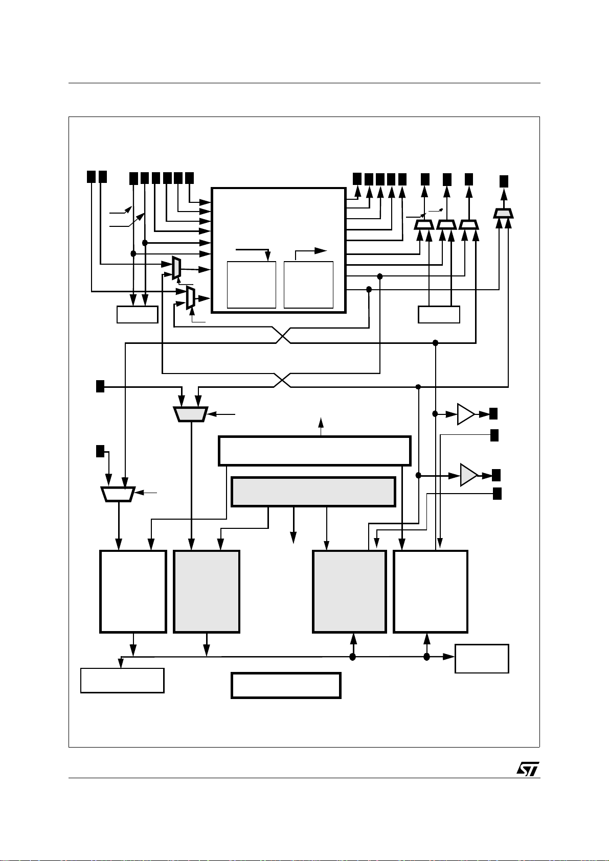
II - BLOCK DIAGRAM
The top level functionalities of
on the general block diagram.
There are:
– The switching ma trix,
– The 2 time slot assigners,
– The 2 x 32 HDLC transmitters with associ ated
DMA controllers,
– The 2 x 32 HDLC receivers with associated
DMA controllers,
– The 16 Command/Indicate and Monitor Channel
transmitters belonging to the two Gene ral Com ponent Interfaces (GCI),
– The 16 Command/Indicate and Monitor Channel
receivers belonging to the two General Component Interfaces (GCI),
– The Synchronous Dyn amic Mem ory interface,
– The microprocessor interface including Write
FIFO and Fetch Memory,
– The bus arbitration,
– The clock selection and time synchronization
function,
– The interrupt controller,
– The watchdog
III - FUNCTIONAL DESCRIPTION
III.1 - The Switching Matrix N x 64 KBits/S
III.1.1 - Function Description
The matrix performs a non-bl ock ing switc h of 256
time slots from 8 Input Time Division Multiplex
(TDM) at 2 Mbit/s to 8 output Time D ivision Mu ltiplex at 2 Mb it/s. A T DM at 2 Mbit/s consist s of 32
Time Slots (TS) at 64 kbit/s. One Time Division
Multiplex at 4 Mbit/s can take place of two Time Division Mu ltiplex at 2 Mbit/s . This TDM at 4 Mbi t/s
is composed of 64 Time Slots (TS) at 64 kbit/s.
The matrix is designed to sw itch a 64 k bit/ s cha nnel (Variable delay mode) or an hyperchannel of
data (Sequence integrity mode). So, it will both
provide minimum throughput switching delay for
voice applications and time slot sequence integrity
for data applications on a per channel basis.
The requirements of the Sequence I ntegrity (n*64
kbit/s) mode are the following:
All the time slots of a given input frame must be put
out during a same output frame.
The time slots of an hyperchannel (concatenation
of TS in the same TDM) are not crossed together
at output in different frames.
In variable delay mode, the time slot is put out as
soon as possible. (The delay is two or three time
slots minimum between input and output).
Multi-HDLC
appear
For test facilities, any time slot of an Output TDM
(OTDM) can be internally looped back into the
same Input TDM number (ITDM) at the same time
slot number.
A Pseudo Random Sequence Generator and a
Pseudo Random Sequence Analyser are implemented in the matrix. They allow the generation of
a sequence on a channel or on a hyperchannel, to
analyse it and verify its integrity after several
switching in the matrix or some passing of the sequence across different boards.
The Frame Signal (FS) synchronises ITDM and
OTDM but a programmable delay or advance can
be introduced separately on each ITDM and
OTDM (a half bit time, a bit time or two bit times).
An additional pin (PSS) permits the generation of
a programmable signa l composed of 256 bits per
frame at a bit rate of 2048 kbit/s. The programmation of this signal is performed thanks to PS bit of
Connection Memory.
An external pin (NDIS) asserts a h igh impedance
on all the TDM out puts of the matrix when active
(during the initialization of the board for example).
III.1.2 - Architecture of the Matrix
The matrix is essentially composed of buffer data
memories and a Connection Memory.
The received serial data is first converted to parallel by a serial to parallel converter and stored consecutively in a 256 position Buf fer Data Memory
(see Figure).
To satisfy the Seque nce Integrity (n*6 4 kbit/s) requirements, the data memory is built with an even
memory, an odd mem ory and an out put mem ory.
Two consecutive frames are stored alternatively in
the odd and even memory. During the time an input frame is stored, the one previously stored is
transferred into the output memory according to
the connection memory switching orders. A frame
later, the output memory is read and data is converted to serial and transferred to the output TDM.
III.1.3 - Connection Fu nct i on
Two types of connections are offered:
– unidirectional connec tion and
– bidirectional connec t ion.
An unidirectional connection makes only the
switch of an input t ime s lo t through an output one
whereas a bidirectional connection establishes the
link in the other direction too. So a double connection can be achieved by a single comm and (see
Figure).
13/130
Page 14
STLC5466
Figure 1 :
DIN 6
DIN 7
GCI1
DIN 9
DIN 8
BLOCK DIAGRAM
DIN 3
DIN 4
DIN 5
GCI0
RX GCI
DIN 2
DIN 1
DIN 0
D6
SWIT C H ING MA TRIX
0
1
2
3
4
n x 64 kb/s
Scrambler/Descrambler
for 32 channels
5
Pseudo
6
Random
Sequence
7
Analyser
D7
V10b
FIRST TIME SLOT ASSIGNER
Pseudo
Random
Sequence
Generator
0
1
2
3
4
5
6
7
V10a
NDIS
DOUT 0
DOUT 1
DOUT 2
DOUT 3
GCI0
DOUT 4
GCI1
TX GCI
DOUT 6
DOUT 5
V10a
DOUT 7
V10b
CB1
EC1
CB2
FIRST
32 RX HDLC
with Address
Recognition
32 RX DMAC
Microprocessor
interface
14/130
V10a
SECOND
32 RX HDLC
with Address
Recognition
32 RX DMAC
SECOND TIME SLOT ASSIGNER
V10b
SECOND
32 TX HDLC
with C SMA CR
for Contention
Bus
32 TX DMAC
Internal Bus
BUS ARBITRATION
EC2
FIRST
32 TX HDLC
with CSMA CR
for Contention
Bus
32 TX DMAC
SDRAM
Controller
V10a, bit V10 of TADR1
V10b, bit V10 of TADR2
D6, bit of GCR2
D7, bit of GCR1
Page 15

STLC5466
III.1.4 - Loop Back Function
Any time slot of an Output TDM can be internally
looped back on the t ime slot wh ich has the same
TDM number and the same TS number
(OTDMi, TSj) ----> (ITDMi, TSj).
In the case of a bidirect ional connection, onl y the
one specified by the microprocessor is concerned
by the loop back (see Figure).
III.1.5 - Delay through the Matrix
III.1.5.1 - Variable Delay Mode
In the variable delay mode, the delay through the
matrix depends on t he relat ive posi tions of t he i nput and output time slots in the frame.
So, some limits are fixed:
– the maximum del ay is a frame + 2 time slots,
– the minimum delay is programmable.
Three time slots if IMTD = 1, in this case n = 2 in
the formula hereafter or
two time slots if IMTD = 0, in this case n = 1 in
the same formula (see Paragraph “Switching
Matrix Configuration Register SMCR (0C)
”).
H
All the possibilities can be ranked in three cases:
a) If OTSy > ITSx + n then the variable delay is:
OTSy - ITSx Time slots
b) If ITSx
<
OTSy < ITSx+n then the variable delay
is:
OTSy - ITSx + 32 Time slots
c) OTSy < ITSx then the variable delay is:
32 - (ITSx - OTSy) Time slots.
N.B. Rule b) and rule c) are identical.
For n = 1 and n = 2, (see Figure).
III.1.5.2 - Sequence Integrity Mode
In the sequence integrity mode (SI = 1, bit located
in the Connection Memory), the input time slots
are put out 2 frames later (see Figure). In this
case, the delay is defined by a single expression:
Constant Delay = (32 - ITSx) + 32 + OTSy
So, the delay in sequence i ntegrity mode varies
from 33 to 95 time slots.
III.1.6 - Connection Memory
III.1.6.1 - Description
The connection memory is composed of 256 locations addressed by the number of OTDM and T S
(8x32).
Each location permits:
– to connect each input time slot to one output
time slot (If two or more output time slots are
connected to the same input time slot number,
there is broadcasting).
– to select the variable delay mode or the se-
quence integrity mode for any time slot.
– to loop back an output time slot. In this case the
contents of an i nput time slot (ITSx, ITDMp) is
the same as the output time slot (OTSx, OTDMp).
– to output the contents of the corresponding con-
nection memory instead of the data which has
been stored in data memory.
– to output the sequenc e of the pseudo random
sequence generator on an output time slot: a
pseudo random sequence can be inserted in
one or several time slots (hyperchannel) of the
same Output T DM; this insertion must be enabled by the microprocessor in the configuration
register of the matrix.
– to define the source of a sequence by the pseu-
do random sequence analyser: a pseudo random sequence can be extracted from one or
several time slots (hyperchannel) of the same
Input TDM and rout ed to the analyser; this extraction can be en abled by the microprocessor
in the configuration register of the m atrix (SMCR).
– to ass ert a high impedance level on an output
time slot (disconnection).
– to deliver a programmable 256-bit sequence
during 125 microseconds on the Programmable
synchronization Signal pin (PSS).
III.1.6.2 - Access to Connection Memory
Supposing that the Switching Matrix Configuration
Register (SMCR) has been already written by t he
microprocessor, it is possi ble to access to the connection memory from microprocessor with the
help of two registers:
– Connection Memory Data Register (CMDR) and
– Connection Memory Address Register (CMAR).
III.1.6.3 - Access to Data Memory
To extract the contents of the data memory it is
possible to read the data memory from microprocessor with the help of the two registers:
– Connection Memory Data Register (CMDR) and
– Connection Memory Address Register (CMAR).
III.1.7 - Switching at 32 Kbit/s
Four TDMs can be programmed individually to
carry 64 channels at 32 Kbit/s (only if these TDMs
are at 2 Mbit/s).
Two bits (SW0/1) located in SMCR define the type
of channels of two couples of TDMs.
SW0 defines TDM0 and TDM4 (GCI0) and SW1
defines TDM1 and TDM5 (GCI1).
If TDM0 or/and TDM1 carry 64 channels at 32
15/130
Page 16

STLC5466
Kbit/s then TDM2 or/and TDM3 are not available
externally they are used internally to perform the
function.
See figure: Downstream switching at 32 kb/s.
See figure: Upstream switching at 32 kb/s.
III.1.8 - Switching at 16 Kbit/s
The TDM4 and TDM5 can be GCI multiplexes.
Each GCI multiplex comprises 8 GCI channels.
Each GCI channel comprises one D channel at 16
Kbit/s. See figure: GCI channel definition, GCI
Synchro signal delivered by the Multi-HDLC
It is possible to switch the contents of 16 D channels from the 16 GCI channels to 4 timeslots of the
256 output timeslots.
In the other di rection the cont ents of an sel ected
timeslot is automatically switched to 4 D channels
at 16 Kbit/s.
See Connection Memory Data Register CMDR
(0E)H.
III.2 - HDLC CONTROLLER
III.2.1 - Function description
Two independent HDLC controllers allow to process 64 channels.
Each internal HDLC controller can run up to 32
channels in a conventional HDLC mode or in a
transparent (non-HDLC) mode (configurable per
channel).
Each channel bit rate is programmable from 4kbit/
s to 64kbit/s. All the configurations are also possible from 32 cha nnels (from 4 to 6 4 kbit/s) to one
channel at 2 Mbit/s.
– First HDLC controller
In reception for the first HDL C cont roller, the co ntents of each time slot can directly come from the
input TDM DIN8 (direct H DLC Input) or from a ny
other TDM input after switching t owards the output
7 of the matrix (configurable per time slot).
In transmission, the HDLC frames are sent on the
output DOUT6 and on the output CB1 (with or
without contention mechanism), or are switched
tow ar ds th e ot her TD M out put vi a th e in put 7 of th e
matrix.
– Second HDLC controller
In reception for the second HDLC c ontroller, the
contents of each time slot can directly com e from
the input TDM DIN9 (direct HDLC Input) or from
any other TDM input after switching towards the
output 6 of the matrix (configurable per time slot).
In transmission, the HDLC frames are sent on the
output DOUT7 and on the output CB2 (with or
without contention mechanism), or are switched
towards the other TDM output via the input 6 of the
matrix .
III.2.1.1 - Format of the HDLC Frame
The format of an HDLC frame is the s ame in receive and transmit direction and shown here after.
III.2.1.2 - Composition of an HDLC Frame
Opening Flag
Address Field (first byte)
Address Field (second byte)
Command Field (first byte)
Command Field (second byte)
Data (first byte)
Data (optional)
Data (last byte)
FCS (first byte)
FCS (second byte)
Closing Flag
– Opening Fl ag
– One or two bytes for address recognition (recep-
tion) and insertion (transmission)
– Data bytes with bit stuffing
– Frame Check S equence: CRC with polynomial
G(x) = x
16
+x12+x5+1
– Closing Flag.
III.2.1.3 - Description and Functions of the
HDLC Bytes
–FLAG
The binary sequence 01111110 m arks the be-
ginning and the end of the HDLC Frame.
Note: In reception, three possible flag configura-
tion are allowed and correctly detected:
- two normal consecutive flags:
...01111110 01111110...
- two consecutive flags with a “0” common:
...011111101111110...
- a global common flag:...01111110...
this flag is the closing flag for the current frame
and the opening flag for the next frame
– ABORT
The binary sequence 11111 11 marks an Abort
command.
In reception, seven consecutive 1’s, inside a
message, are detected as an abort command
and generates an interrupt to the host.
In transmit direction, an abort is sent upon com-
mand of the micro-processor. No ending flag is
expected after the abort command.
16/130
Page 17

STLC5466
– BIT STUFFING AND UNSTUFFING
This operation is done to avoid the c on fusio n of
a data byte with a flag.
In transmission, if five consecutive 1’s appear in
the serial stream being transmitted, a zero is automatically inserted (bit stuffing) after the fifth
“1”.
In reception, if five consecutive “1” followed by a
zero are received, the “0” is assumed to have
been inserted and is automatically deleted (bit
unstuffing).
– FRAME CHECK SEQUENCE
The Frame Check Sequence is calculated according to the recommendation Q921 of the
CCITT.
– ADDRESS RECOGNITION
In the frame, one or two bytes are transmitted to
indicate the destination of the message. Two
types of addresses are possible:
- a specific destination address
- a broadcast address.
In reception, the controller compares the receive
addresses to internal registers, which contain
the address message. 4 bits in the receive command register (HRCR) inform the receiver of
which registers, it has to take into account for the
com parison. The rece iver compar es th e two address bytes of the message to the specific board
address and the broadcast address. Upon an
address match, the address and the data following are written to the data buffers ; upon an address mismatch, the frame is ignored. So, it
authorizes the filtering of the messages. If no
comparison is specified, each frame is received
whatever its address field.
In Transmission, the controller sends t he frame
including the destination or b roadcast addresses.
III.2.2 - CSMA/CR Capability
An HDLC channel can come in and go out by any
TDM input on the matrix.
For time constraints, direct HDLC Access is
achieved by the input TDM (DIN 8 for the first
HDLC controller and DIN9 for the second HDLC
controller) and the output TDM (DOUT6 for the
first and DOUT7 for the second HDLC controller).
In transmission, a time slot of a TDM can be
shared between different s ources in Multi-point to
point configuration (different subscriber’s boards
for example). The arbit ratio n system is the CSMA/
CR (Carrier Sense Multiple access with Contention Resolution).
The contention is resolved by a bus connected to
the CB1 pin (Contention Bus) for t he first HDLC
controller and CB2 pin for the second HDLC con-
troller. These two bus are respe ctively a 2Mbit/s
wire line common to all the potential sources.
If the first HDLC controller (or the second) has obtained the access t o the bu s, the data to transmit
is sent simultaneously on the CB1 line (or the CB2
line) and the output TDM. The result of the contention is read back on the Echo line (EC1o r EC2). If
a collision is detected, the transmission is stopped
immediately. A contention on a bit basis is so
achieved. Each message to be sent with CSMA/
CR has a priority class (PRI = 8, 10) indicated by
the Transmit Descriptor and some rules are implemented to arbitrate the access to the line. The
CSMA/CR Algorithm is given. Whe n a request to
send a message occurs, the transmitter determines if the shared channel is free. The
HDLC
listens to the Echo line. If C or more consecutive “1” are detected (C depending on the message’s priority), the
message. Each bit sent is sampled back and compared with the original value to send. If a bit is different, the transmission is instantaneously
stopped (before the end of this bit time) and will restart as soon as the
channel is free without interrupting the microprocessor.
After a successful transmi ssion of a message, a
programmable pen alty PEN(1 or 2) is applied to
the transmitter. It guarantees that the same transmitter will not take the b us another time b efore a
transmitter which has to send a message of same
priority.
In case of a collision, the frame which has been
aborted is automatically retransmitted by the DMA
controller without warning the microprocessor of
this collision. The frame can be located in several
buffers in external memory. The collision can be
detected from the second bit of the opening frame
to the last but one bit of the closing frame.
III.2.3 - Ti m e Slot Assigner Memory
Each HDLC channel is bidirectional and is defined
by two Time Slot Assigners (TSA).
TSA is a memory of 32 words (one per phys ical
Time Slot) where all of the 32 input and output time
slots of the HDLC controllers can be associated to
logical HDLC channels. Super channels are created by assigning the same logical chann el num ber
to several physical time slot s.
The following features are programmed for each
HDLC time slot:
– Time slot used or not
– One logical channel number
– Its so u r ce:
- DIN 8 or the output 7 of the matrix for the first
Time Slot Assigner
Multi-H DLC
Multi-HDLC
begins to send its
will detect that the
Multi-
17/130
Page 18

STLC5466
- DIN 9 or the output 6 of the matrix for the second Time Slot Assigner.
– Its bit rate and conc erned bit s (4k bit/s to 64kbit /
s). 4kbit/s correspond to one bit transmitted
each two frames. This bit is repeated twice in
transmission. This bit must be present in two
consecutive frames in reception.
– Its destination for the first Time Slot Assigner:
- direct output on DOUT6
- direct output on DOUT6 and on the Contention
Bus (CB1)
- on another OTDM via input 7 of the matrix and
on the Contention Bus (CB1)
– Its destination for the second Time Slot Assig n-
er:
- direct output on DOUT7
- direct output on DOUT7 and on the Contention
Bus (CB2)
- on another OTDM via input 6 of the matrix and
on the Contention Bus (CB2)
III.2.4 - Data Storage Structure
Data associated with each Rx and Tx HDLC channel is stored in external memory; The data transfers between the HDLC controllers and m emory
are ensured by 2*32 DMAC (Direct Memory Access Controller) in reception and 2*32 DMA C in
transmission.
The storage structure chosen i n bot h di rections is
composed of one circular queue of buffers per
channel. In such a queue, each data buffer is
pointed to by a Descriptor located in external
memory too. The main information contained in
the Descriptor is the address of the Data Buf fer, its
length and the address of the next Descriptor; so
the descriptors can be linked together.
This struct ur e allow s to:
– Store receive frames of variable and unknown
length
– Read transmit frames stored in external memory
by the host
– Easily perform the frame relay function.
III.2.4.1 - Reception
At the initialization of the application, the host has
to prepare two Initialization Block registers. Each
Initialization Block located in shared memory contains the first receive buffer descriptor address for
each channel, and the receive circular queues. At
the opening of a receive channel, the DMA controller reads the address of the first buffer descriptor corresponding to this channel in the
initialization Block. Then, the data transfer can occur without intervention of the processor.
A new HDLC frame always begins in a new buffer.
A long frame can be split between several buffers
if the buffer size is not sufficient. All the information
concerning the fram e a nd its l ocatio n in the c ircular queue is included in the Receive Buffer Descriptor:
– The Receive Buffer Address (RBA),
– The size of the receive buffer (SOB),
– The number of bytes written into the buffer
(NBR),
– The Next Receive Descriptor Address (NRDA),
– The status concerning the receive frame,
– The control of the queue.
III.2.4.2 - Transmission
In transmission, the data is manage d by a sim ilar
structure as in reception
By the same way, a frame can be split up between
consecutive transmit buffers.
The main information contained in the Transmit
Desc rip t or ar e:
– transmit buffer address (TBA),
– number of bytes to transmit (NBT) concerning
the buffer,
– next transmit descriptor address (NTDA),
– status of the frame after transmission,
– control bit of the queue,
– CSMA/CR priority (8 or 10).
III.2.4.3 - Frame Relay
The principle of the frame relay is to transmit a
frame which has been received without treatment.
A new heading is just added. This will be easily
achieved, taking into account that the queue structure allows the transmission of a frame s plit between several buffers.
III.2.5 - Transparent Modes
In the transparent mode, the
data in a completely transparent manner without
performing any bit manipulation or Flag insertion.
The transparent mode is per byte function; the
channel used for this mode is n*64 kb/s mandatory.
Two transparent modes are offered:
– First mode: for the receive channels, the
HDLC
continu ously w rites rece ived b ytes (from
the received timeslot) into the external memory
as specified in the current receive descriptor
without taking into account the Fill Character
Register.
– Second mo de: the Fill Character Register spec-
ifies the “fill c ha ra c te r” w hic h m u st be tak en int o
account. In reception, the “fill character” is de-
Multi-HDLC
transmits
Multi-
18/130
Page 19

STLC5466
tected in each timeslot and will not be transferred to the external memory. The detection of
“Fill character” marks the end of a message and
generates an interrupt if BINT=1). When the “Fill
character” is not detected a new message is re-
ceiving.
As for the HDLC mode the correspondence between the physical time slot and the logical channel is fully defined in the two Time Slot Assigners
(Time slot used or not used, logical channel
number, source, destination).
III.2.6 - Command of the HDLC Channels
The microprocessor is able to control each HDLC
receive and transmit channel. Some of the com mands are specific to the transmission or t he reception but others are identical.
III.2.6.1 - Reception Control
– The configuration of the controller operating
mode is: HDLC mode or Transparent mode.
– The control of the controller: START, HALT,
CONTINUE, ABORT.
START: On a start comm and, the RxDM A con-
troller reads the address of the first descriptor in
the initialization block memory and is ready to
receive a frame.
HALT: For overloading reasons, the microproc-
essor can decide to halt the reception. The DMA
controller finishes transfer of the current frame
to external memory and stops. The channel can
be restarted on CONTINUE command.
CONTINUE: The reception restarts in the next
descriptor.
ABORT: On an abort command, the reception is
instantaneously stopped. The channel can be
restarted on a START or CONTINUE command.
– Reception of FLAG (01111110) or IDLE
(11111111) between Frames.
– Address recognition. The microprocessor de-
fines the addresses that the Rx controller has to
take into account.
– In transparent mode: “fill character” register is
selected or not.
III.2.6.2 - Transmission Control
– The configuration of the controller operating
mode is: HDLC mode or Transparent mode.
– The control of the controller: START, HALT,
CONTINUE, ABORT.
START: On a start comm and, t he Tx DM A controller reads the address of the first descriptor in
the initialization block memory and tries to transmit the first frame if End Of Queue is not at “1”.
HALT: The transmitter finishes to send the current frame and stops.The channel can be restarted on a CONTINUE command.
CONTINUE: if the CONTINUE command occurs
after HALT command, the HDLC Transmitter restarts by transmitting t he next bu ffer as sociat ed
to the next descriptor.
If the CONTINUE command occurs after an
ABORT command which has occurred during a
frame, the HDLC transmitter restarts by transmitting the frame which has been effectively
aborted by the microprocessor.
ABORT: On an abort comm and, the transmission of the current frame is instantaneously
stopped, an ABORT sequence “1111111” is
sent, followed by IDLE or FLAG bytes. The
channel can be restarted on a START or CONTINUE command.
– Transmission of FLAG (01111110) or IDLE
(111111111) between frames can be selected.
– CRC can be generat ed or no t. If the CRC is not
generated by the HDLC Controller, it must be located in the shared memory.
– In transparent mode: “fill character” register can
be selected or not.
III.3 - C/I and Monitor
III.3.1 - Function Description
The
Multi-HDLC
is able to operate both GCI and
V* links. The TDM DIN/DOUT 4 and 5 are internally connected to the CI and Monitor receivers/transmitters. Since the controllers handle up to 16CI
and 16 Monitor channels simultaneously, the
ti-HDLC
The
can manage up to 16 level 1 circuits.
Multi-H D L C
can be used to support the CI and
Mul-
monitor channels based on the following protocols:
– ISDN V* protocol
– ISDN GCI protocol
– Analog GCI protocol.
III.3.2 - GCI and V* Protocol
A TDM can carry 8 GCI channels or V* channels.
The monitor and S/C bytes always stand at the
same position in the TDM in both cases.
CGI Channel 0
TS0 TS1 TS2 TS3 TS28 TS29 TS30 TS31
B1 B2 MON S/C B1 B2 MON S/C
CGI Channel 1 to Channel 6
CGI Channel 7
19/130
Page 20
STLC5466
The GCI or V* channels are composed of 4 bytes
and have both the same general structure.
B1 B2 MON S/C
B1, B2 : B ytes of data. Those bytes are not af-
fected by the monitor and CI protocols.
MON : Monitor channel for operation and
maintenance information.
S/C : Signalling and control information.
Only Monitor hands hakes and S/C bytes are dif-
ferent in the three protocols:
ISDN V* S/C byte
D 2 bits C/I 4 bits T E
ISDN GCI S/C byte
D 2 bits C/I 4 bits A E
Analog GCI S/C byte
C/I 6 bits A E
CI : The Comm and/Indicate channel is used for
activation/deactivation of lines and control
functions.
D : These 2 bits carry the 16 kbit/s ISDN basic
access D channel.
In GCI protocol, A and E are the handshake bits
and are used to control the transfer of information
on monitor channels.The E bit indicates the transfer of each new byte in one direction and the A bit
acknowledges this byte transfer in the reverse direction.
In V* protocol, there isn’t any handshake
mode.The transmitter has only to mark the validity
of the Monitor byte by positioning the E bit (T is not
used and is forced to “1”).
For more information about the GCI and V*, ref er
to the General Interface Circuit Specification
(issue1.0, march 1989) and the France Telecom
Specification about ISDN Basic Access second
generation (November 1990).
III.3.3 - Structure of the Treatment
In reception GCI/V* TDM’s are connected to DIN 4
and DIN 5. The D channel s are switched t hrough
the matrix towards the output 7 and output6 then
towards the HDLC receivers. The Monitor and S/C
bytes are multiplexed and sent to the CI and Monitor receive rs .
In transmission, the S/C and Monitor bytes are recombined by multiplexing the information provided
by the Monitor, C/I and the HDLC Transmitter.
Like in reception, the D channel is switched
through the matrix (input 7 towards DOUT 4 and
DOUT 5).
III.3.4 - CI and Monitor Channel Configuration
Monitor channel data is located in a time slot; the
CI and monitor handshake bits are in the next time
slot.
Each channel can be defined independently. A table with all the possible configurations is presented hereafter (Table 13).
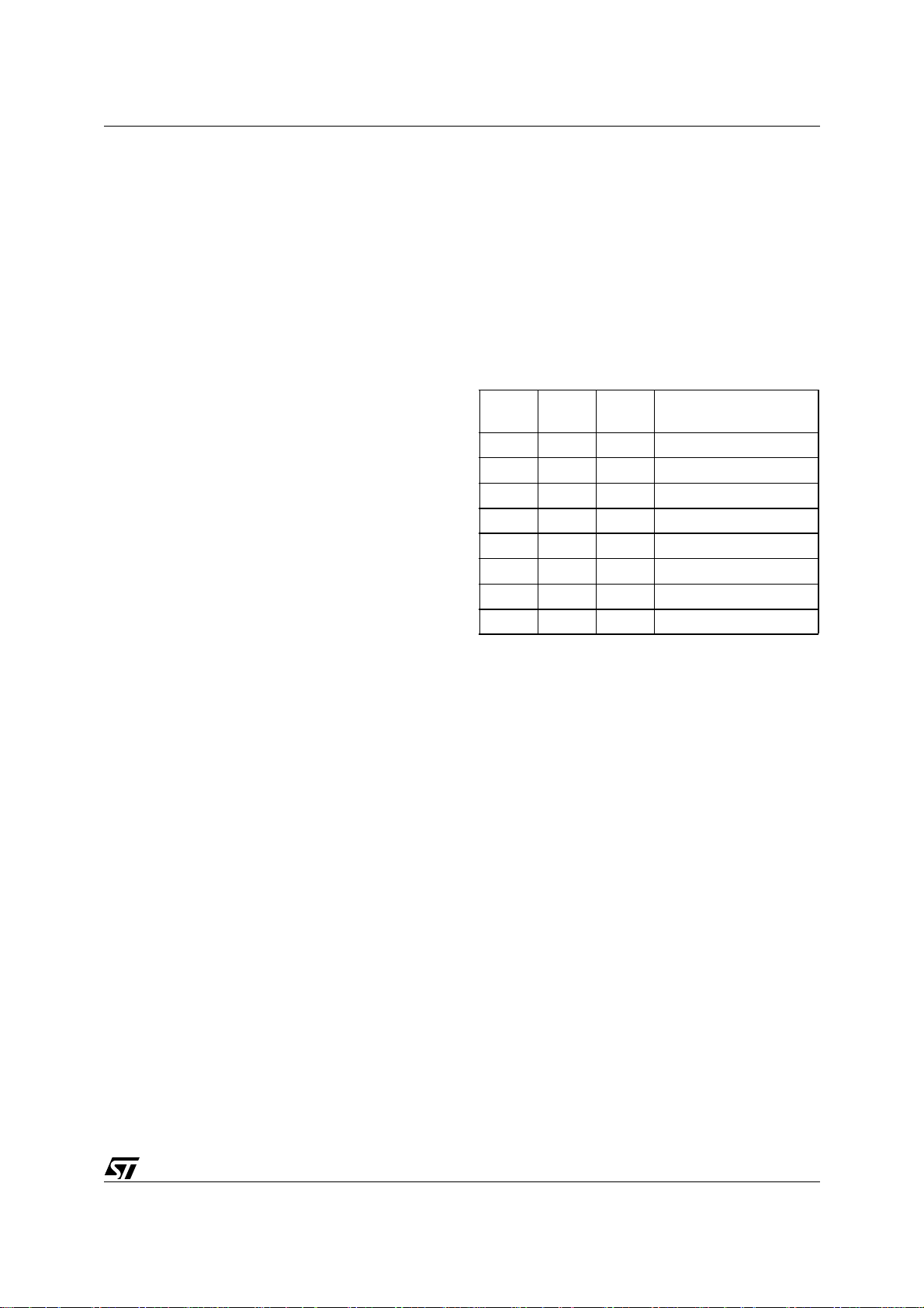
Table 13: C/I and MON Channel Configuration
C/I validated
or not
Monitor validated
or not
Note:
A mix of V* and GCI monitoring can be performed for two dis-
tinct chan nels in the sam e applicat io n.
CI For analog subscriber (6 bits)
CI For ISDN subscriber (4 bits)
Monitor V*
Monitor GCI
III.3.5 - CI and Monitor Transmission/Reception
Command
The reception of C/I and Monitor messages are
managed by two interrupt queues.
In transmission, a transmit command register is
implemented for each C/I and monitor channel
(16C/I transmit command registers and 16 Monitor
transmit command regist ers). Those regist ers are
accessible in read and write modes by the microprocessor.
III.4 - Scrambler and Descrambler
The TDM4 and TDM5 can be GCI multipexes.
Each GCI multipex comprises 8 GCI channels.
Each GCI channe l comprises two B chann els at
64 Kbit/s.
In reception it is possible to switch and to scramble
the contents of 32 B channels of GCI channels to
32 timeslots of the 256 output timeslots. In transmission these 32 timeslots are assigned to 32 B
channels.
In the other direction the contents of an selected B
channels is automatically switched an d descrambled to one B channel of 16 GCI channel.
See SCR bit of Connection Memory Data Register
CMDR (0E)H.
III.5 - Connection between “ISDN channels”
and GCI channels.
Three timeslots are assigned to one “ISDN channels”. Each “ISDN channels” comprises three
channels: B1+B2+B* with B*= D1,D2, A, E, S1,
S2, S3, S4 (See figure).
– Upstream. From GCI channels to ISDN chan-
nels.
• in reception: 16 GCI channels (B1+B2+MON+
D+C/I),
20/130
Page 21
STLC5466
• in transmission: 16 ISDN channels (B1+B2+B*).
It is possible to swit ch t he c ontents of B 1, B2 and
D channels from 16 GCI channels in any 16 “ISDN
channels”, TDM side.
The contents of B1 and/or B2 can be scrambled or
not. If scrambled the number of the 32 timeslots
(TDM side) are different mandatory.
Receiving the contents of M onitor and Command
/ Indicate channels from 16 G CI channels. Pr imitives and messages are stored automatically in
the external shared memory.
Transmitting “six bit word” (A, E, S1, S2, S3, S4)
to any 16 “ISDN channels” TDM side or not. See
SBV bit of General Configuration Register GCR
(02)H.
– Downstream. From ISDN channels to GCI chan-
nels.
• in reception: ISDN channel (B1+B2+B*)
• in transmission: GCI channel (B1+B2+MON+
D+C/I)
It is possible to swit ch t he c ontents of B 1, B2 and
D channels from 16 “ISDN channels”, TDM side in
16 GCI channels.
The contents of B1 and/or B2 can be descrambled
or not. If descrambled the 32 B1/B2 belong to GCI
channels mandatory.
Receiving six bit word (A, E, S1, S2, S3, S4) from
any 16 “ISDN channels”, TDM side. The 16 “six bit
word” are stored automatically in the external
shared memory.
Transmitting the contents of Monitor and Command / Indicate channels to 16 GCI channels. See
SBV bit of General Configuration Register GCR
(02)H.
– Alarm Indication Signal.
This detection concerns 16 hyperchannels. One
hyperchannel comprises 16 bits (B1 and B2 only).
The Alarm Indications for the 16 hyperchannels
are stored automatically in the external shared
memory. See AISD bit of Switchi n g Matrix C onfiguration Register SMCR (0C)H.
III.6 - Microprocessor Interface
III.6.1 - Description
Multi-HDLC
The
circuit can be controlled by several types of microprocess ors (ST9/10, Intel /Motorola 8 or 16 data bits interfaces) such as:
– ST9/10 fa mily
– INTEL 80C188 8 bits
– INTEL 80C186 16 bits
– INTEL 386EX 16 bits
– MOTOROLA 68000 16 bits
– MOTOROLA 68020 32 bits
Table 14 :
MOD2
Pin
During the initialization of the
Microprocessor Interface Selection
MOD1
Pin
0 1 1 80C188
1 1 1 80C186
1 0 0 68000
0 0 0 68020
0 0 1 ST9
1 0 1 ST10 A/D multiplexed
1 1 0 ST10 A/D Not multiplexed
0 1 0 386EX
MOD0
Pin
Microprocessor
Multi-HD LC
circuit,
the microprocessor interface is informed of the
type of microprocessor that is connected by polarisation of three external pins MOD 0/2.
Three chip Select (CS0/2) pins are provided. CS0
will select the internal registers and CS1 the external memory. CS2 can be used to select the external memory in INTEL 386EX application only (see
pin 41 definition).
III.6.2 - Buffer
A Buffer is located in the microprocessor interface.
It is used whatever microprocessor selected
thanks to MOD0/2 pins. It allows to reduce the
shared memory access cycles for the microprocessor.
This Buffer consists of o ne Write FIFO and one
Read Fetch Memory (see Figure).
III.6.2.1 - Write FIFO
When the microprocessor delivers the address
word named Ax to write dat a named [Ax] in the
shared memory in fact it writes data [Ax] and address word Ax in the Write FIFO (8 words). If Ax is
in Fetch Memo r y, [Ax ] is re moved i n Fetch Memory.
There is no wait time for the microprocessor if the
Write FIFO is not full entirely.
21/130
Page 22
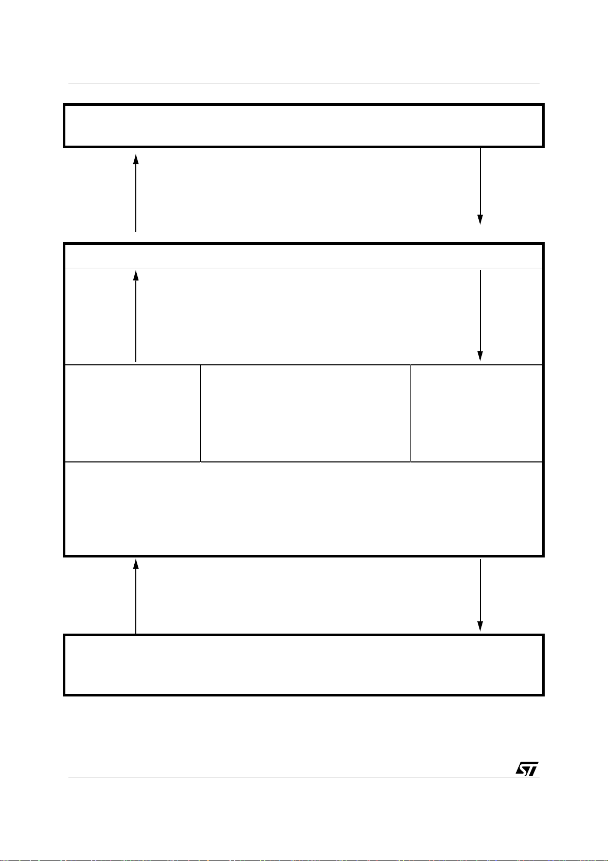
STLC5466
Shared memory
SDRAM Bus
To shared memory SDRAM Controller From shared memory
MHDLC Internal Bus
Ax, [Ax] Read Fetch 64 words
Ay, [Ay] Memory
Az, [Az]
At, [At] Write FIF O
Up to eight wo rds
Input register used to
store data in Write
FIFO
from microprocessor
Fetch Memory
An, [An]
MHDLC microprocessor interface To microprocessor
Microprocessor Bus
Microprocessor
Figure 2 :
22/130
Exchange between Microprocessor and Shared memory across MHDLC
Page 23
STLC5466
III.6.2.2 - Read Fetch Memory
When the microprocessor delivers the address
word named An to read data named [An] out of the
shared memory in fact it reads data [An] from the
Read Fetch Memory (64 words).
The number of wait cycle f or the microp rocessor i s
strongly reduced. If An, address word delivered by
the microprocessor, and data [An] are already in
the Read Fetch Memory and validated then there
is no wait time for the microprocessor.
The source of [An] is truly the shared memory
whatever An.
Data [An] if validated in Fetch Memory and Data
[An] in shared memory are always the same.
III.6.2.3 - Definition of the Interface for the different microprocessor s
The signals connected to the microprocessor interface are presented on the following figures for
the different microprocessor (see Figures).
III.7 - Memory Interface
III.7.1 - Function Description
The memory interface allows the connection of
Synchronous Dynamic RAM. The memory interface will address up to 16 Megabytes. The memory location is always organized in 16 bits.
The memory is shared b etween the
Multi-HDLC
and the microprocessor. The access to the m emory is arbitrated by an internal function of the c ircuit: the bus arbitration.
III.7.2 - Choice of memory versus microprocessor and capacity required
The memory interface depends on the memory
chips which are connected. The memory chips will
be chosen versus their organization.
Example1: if the applicat ion requires 8 or 16 bit
µ
Processor and 1 Megaword Shared memory
size, one capability is offered:
– 1 SDRAM Circuit (1Mx16).
Example2: if the application requires 16 bit µProc-
essor and 4 Megaword Shared memory size,
three capabilities are offered:
– 4 SDRAM Circuits (1Mx16) or
– 4 SDRAM Circuits (4Mx4) or
– 1 SDRAM Circuit (4Mx16).
.Example3: if the application requires 8 Megaword
Shared memory size three capabilities are offered:
– 8 SDRAM Circuits (4Mx4) or
– 2 SDRAM Circuits (4Mx16) or
– 2 SDRAM Circuit (8Mx8).
III.7.3 - Memory Cycle
Some parameters are frozen:
– Burst Read and Singl e Write.
– The Burst Length is 4.
– The burst data is addressed in sequential mode.
The programmable parameters are:
– Latency Mode
– selected c ircuit organisation
– the exchanges between Multi-HDLC and
SDRAM are at the Master Clock frequency
(33MHz, 50MHz, 66MHz)
III.7.4 - Memories composed of different circuits
III.7.4.1 - Memory obtained with 1M x16 SDRAM
circuit
Signals A22 A21 Signals
NCE3 1 1
NCE2 1 0
NCE1 0 1 UDQM 1
NCE0 0 0 LDQM 0
A0
or equiva-
lent
The Address bits delivered by the Multi-HDLC for
1M x 16 SDRAM circuits are:
– ADM 11 for B ank s el ect correspon ding with A20
delivered by the microprocessor
– ADM0/10 for Row address inputs corresponding
with A9/19 delivered by the microprocessor
– ADM0/7 for Column address inputs correspond-
ing with A1/8 delivered by the microprocessor
III.7.4.2 - Memory obtained with 2M x 8 SDRAM
circuit
Signals A0 or equivalent NLDS NUDS
UDQM 1 0 1
LDQM 0 1 0
The Address bits delivered by the Multi-HDLC for
2M x 8 SDRAM circuits are:
– ADM 11 for B ank s el ect correspon ding with A21
delivered by the microprocessor
– ADM0/10 for Row address inputs corresponding
with A10/20 delivered by the microprocessor
– ADM0/8 for Column address inputs correspond-
ing with A1/9 delivered by the microprocessor
23/130
Page 24
STLC5466
III.7.4.3 - Memory obtained with 8M x 8 SDRAM
circuit
Signals A0 or equivalent NLDS NUDS
UDQM 1 0 1
LDQM 0 1 0
The Address bits delivered by the Multi-HDLC for
8M x 8 SDRAM microprocessor circuits are:
– ADM12/13 for Bank select corresponding with
A22/23 delivered by the microprocessor
– ADM0/11 for Row address inputs corresponding
with A10/21 delivered by the microprocessor
– ADM0/8 for Column address inputs correspond-
ing with A1/9 delivered by the microprocessor
III.7.4.4 - Memory obtained with 4M x 16
SDRA M c i rc uit
Signals A23 Signals
NCE1 1 UDQM 1 0 1
NCE0 0 LDQM 0 1 0
A0 or
equiva-
lent
NLDS NUDS
The Address bits delivered by the Multi-HDLC for
4M x 16 S DRAM circuits are:
– ADM12/13 for Bank select corresponding with
A21/22 delivered by the microprocessor
– ADM0/11 for Row address inputs corresponding
with A9/20 delivered by the microprocessor
– ADM0/7 for Column address inputs correspond-
ing with A1/8 delivered by the microprocessor
III.8 - Bus Arbitration
The Bus arbitration function arbitrates t he access
to the bus b etwe en dif ferent ent ities of the circuit.
Those entities which can cal l for the bus are the
follo wing :
– The receive DMA controller,
– The microproces sor,
– The transmit DMA controller,
– The Interrupt controller,
– The memory interface for refreshing the
SDRAM.
This list gi ves the memory access pri orities per default.
If the treatment of more than 64 HDLC channels is
required by the application, it is possible to chain
seve ra l
Multi-H DLC
components. That is done
with two external pins (TRI, TRO) and a token ring
system.
The TRI, TRO signals are managed by the bus arbitration function too. When a chip has finished its
tasks, it sends a pulse of 30 ns to the next chip.
III.9 - Clocks
III.9.1 - Clock Distribution Selection and Super-
vision
Two clock distributions are available:
Clock at 4.096 MHz or 8.192 MHz and a synchro-
nization signal at 8 KHz.
The component has to select one of these two dis-
tributions and to check its integrity.
Two other clock distributions are allowed: Clock at
3072 MHz or 6144 MHz and a synchronization signal at 8 KHz.
See General Configuration Register GCR (02)
.
H
DCLK, FSC GCI and FSC V* are o utput on three
external pins of the Multi-HDLC. DCLK is the clock
selected between Clock A and Clock B. FSC, GCI
and FSC V* are functions of the selected distribution and respect the GCI and V* f ram e sy nchronization specifications.
The supervision of t he clock distribution consists
of verifying its availability. The detection of the
clock absence is done in a less than 250 microseconds. In case the clock is absent, an interrupt is
generated with a 4 kHz recurrence. Then the clock
distribution is switched automatica lly up to de tection of couple A or couple B. When a couple is detected the change of clock occurs on a falling edge
of the new selected distribution. Moreover the
clock distribution can be con trolled by the microprocessor thanks to SELB, bit of General Configuration Register.
Depending on the applications, three different signals of synchronization (GCI, V* or Sy) can be provided to the comp onent . Th e c lock A/B frequency
can be a 4096 or 8192 kHz clock. The component
is informed of the synchronization and clocks that
are connected by software.
III.9.2 - VCXO Frequency Synchronization
An external VCXO can be used to provide a clock
to the transmission components. This clock is controlled by the main clock distribution (Clock A or
Clock B at 4096kHz). As the c lock of the transmission component is 15360 o r 16384kHz, a c onfigurable function is necessary.
The VCXO frequency is divided by P (30 or 32) to
provide a common sub-multiple (512kHz) of the
reference frequency CLOCKA or CLOCKB
(4096kHz). The com parison of these two si gnals
gives an error signal which commands the VCXO.
Two external pins are needed to perform this function: VCXO-IN and VCXO-OUT.
24/130
Page 25

STLC5466
III.10 - Interrupt Controller
III.10.1 - Description
Three external pins are used to manage the interrupts generated by the
Multi-HDLC
. The interrupts
have three main sources:
– The operating interrupts generated by the HDLC
receivers/transmitters, the CI receivers and the
monitor transmitters/receivers. INT0 Pin is reserved for this use.
– The interrupt generated by an abnormal working
of the clock distribution. INT1 Pin is reserved for
this use.
– The non-activity of the microprocessor (Watch-
dog). WDO Pin is reserved for this use.
III.10.2 - Operating Interrupts (INT0 Pin)
There are five main sources of operating interrupts
Multi-H DL C
in the
circuit:
– The HDLC receiver,
– The HDLC transmitter,
– The CI receiver,
– The Monitor receiver,
– The Monitor transmitter.
When an interrupt is generated by one of these
functions, the interrupt controller:
– Collects all the information about the reasons of
this interrupt
– Stores them in external memory.
– Informs the microprocessor by positioning the
INT0 pin in the high level.
Three interrupt queues are built in exte rnal mem-
ory to store the information about the interrupts:
– A single queue for the HDLC receivers and
transmitter
– One for the CI receivers
– One for the monitor receiver
The microprocessor takes the interrupts into account by reading the Interrupt Register (IR) of the
interrupt controller.
This register informs the microprocessor of the interrupt source. The microprocessor will have information about the in terrupt source by reading the
corresponding interrupt queue (see Paragraph “Interrupt Register IR(38)
” on Page 74).
H
On an overflow of the circular interrupt queues and
an overrun or underrun o f the different FIFO, the
INT0Pin is activated and the origin of the interrupt
is stored in the Interrupt Register.
A 16 bits register is associated with the Tx Monitor
interrupt. It informs the microprocessor of which
transmitter has generated the interrupt (see Paragraph “Transmit Monitor Interrupt Register
TMIR(30)
” on Page 71).
H
III.10.3 - Time Base Interrupts (INT1 Pin)
The Time base interrupt is generated when an absence or an abnormal working of clock distribution
is detected. The INT1 Pin is activated.
III.10.4 - Emergency Interrupts (WDO Pin)
The WDO signal is activated by an overflow of the
watchdog register.
III.10.5 - Interrupt Queues
There are three different interrupt queues:
– Tx and Rx HDLC interrupt queue
– Rx C/I interrupt queue
– Rx Monitor interrupt queue.
Their length can be defined by software.
For debugging function, each interrupt word of the
CI interrupt queue and monitor interrupt queue
can be followed by a time stamped word. It is composed of a counter which runs in the range of
250µs. The counter is the same as the watchdog
counter. Consequently, the watchdog function
isn’t available at the same time.
III.11 - Watchdog
This function is used to control the activity of the
application. It is composed of a counter which
counts down from an initial value loaded in the
Timer register by the microprocessor.
If the microprocessor doesn’t reset this counter
before it is totally decremented, the external Pin
WDO is activated; this signal can be used to reset
the microprocessor and all the application.
The initial time value of the counter is programmable from 0 to 15s in increments of 0.25ms.
At the reset of the component, the counter i s automatically initialized by the value corresponding t o
512ms which are indicated in the Timer register.
The microprocessor must put WDR (IDCR Register) to”1” to reset this counter and to confirm that
the application started correctly.
In the reverse case, the WDO signal could be used
to reset the board a second time.
III.12 - Reset
There are two possibilities to reset the circuit:
–by software,
– by hardware.
Each programmable register receives its default
value. After that, the default value of each data
register is stored in the associated memory except
for Time slot Assi gn e r memory.
25/130
Page 26

STLC5466
III.13 - BOUNDARY SCAN
The Multi-HDLC is equipped with an IEEE Standard Test Access Port (IEEE Std 1149.1). The
boundary scan technique involves the inclusion of
a shift register stage adjacent to each component
pin so that signa ls at component boundaries can
be controlled and observed using scan testing
principle. Its intention is to enable the test of on
board interconnections and ASIC production tests.
The external interface of the Boundary Scan is
composed of the signals TDI, TDO, TCK, TMS
and TRST as defined in the IEEE Standard.
26/130
Page 27
STLC5466
IV - DC SPECIFICATIONS
Absolute Maximum Ratings
Symbol Parameter Value Unit
V
DD
T
stg
Recommended DC Operating Conditions
Symbol Parameter Min. Typ. Max. Unit
V
DD
T
oper
Note 1:
For 5V tolerant inputs and 5V tolerant output buffers in tristate mode
Note 2:
All the following specifications are valid only within these recommended operating conditions
.
TTL Input DC Electrical Characteristics
Symbol Parameter Test Conditions Min. Typ. Max. Unit
V
IL
V
IH
V
OL
V
OH
I
IL
I
IH
I
oz
Vhyst Schmitt Trigger hysteresis 0.4 0.7 V
V
T+
V
T-
3.3V Power Supply Voltage -0.5V to 4V V
Input or Output Voltage -0.5 to V
+ 0.5V V
DD
Input or Output Voltage -0.5 to +5.5V(see Note 1) V
Storage Temperature -55 to 125 °/C °/C
3.3V Power Supply Voltage (see Note2) 3.0 3.3 3.6 V
Operating Temperature - 40 85 °/C
Low Level Input Voltage 0.8 V
High Level Input Voltage 2.0 V
Low Level Output Voltage IOL = X mA (see Note 3) 0.4 V
High Level Output Voltage IOH = -X mA (see Note 3) 2.4 V
Low Level Input Current
VI = 0V 1 µA
Without pull-up device
High Level Input
Without pull-up device
Tristate output leakage current
VI = V
DD
-1 µA
VI = VDD -1 µA
without pullup/down device
Positive Trigger Voltage 0.9 1. 35 V
Negative Trigger Voltage 0.4 0.7 V
Note 3:
X is the source /sink current under worst case conditions in accordance with the drive capability: O3 = 3mA, O4 = 4 mA
CMOS Output DC Electrical Characteristics
valid only within these recommended operating conditions
Symbol Parameter Test Conditions Min. Typ. Max. Unit
V
IL
V
IH
V
OL
V
OH
Note 4: X is the source/sink curr ent under worst case conditions and is reflect ed i n the name of the I/O cell acc ording to the drive capability.
X = 4 or 8mA
Low level input voltage 0.2VDDV
High level input voltage 0.8V
DD
Low Level Output Voltage Iol = XmA (see Note 4) 0.4 V
High Level Output Voltage Ioh = XmA (see Note 4) 0.85V
DD
V
V
27/130
Page 28
STLC5466
pull-up and pu l l-dow n charact erist ics
Symbol Parameter Test Conditions Min. Typ. Max. Unit
Ipu pull-up current Vi = 0V (Note5) -25 -66 -125 µA
Ipd pull-down current Vi = Vdd (Note5) +25 +66 +125 uA
Ipd pull-down current Vi = 5V (Note5) +25 +66 +125 uA
Rpu Equivalent pull-up resistance Vi = 0V 50 KOhm
Rpd Equivalent pull-down resistance Vi = Vdd 50 KOhm
Rpd Equivalent pull-down resistance Vi = 5V (Note6) 76 KOhm
Note5 Min conditio n: Vdd = 3.0V, 85 degrees C.
Note6 For 5V tolerant buffers
Max condition: Vdd = 3.6V, -40 degrees C.
General interface Electrical Characteristics
Symbol Parameter Test Conditions Min. Typ. Max. Unit
P Power Dissipation VDD=3.3 Volts;
MCLK=66MHz
Cin Input capacitance Freq = 1MHz@0V (Note6) 2 4 pF
Cout Output capacitance (Note
C i/o Bidir I/O capacitance (Note
)4pF
7
)48pF
7
VESD Electrostatic Protection C = 100pF, R = 1.5kΩ 2000 V
Note7 Excluding package (TQ F P176, add 1.9pF)
350 450 mW
28/130
Page 29

STLC5466
V - List of registers
Internal registers
• Identification and Dynamic Command Register IDCR (00)H
• General Configuration Register 1 GCR1 (02)H
• Input Multiplex Configuration Register 0 IMCR0 (04)H
• Input Multiplex Configuration Register 1 IMCR1 (06)H
• Output Multiplex Configuration Register 0 OMCR0 (08)H
• Output Multiplex Configuration Register 1 OMCR1 (0A)H
• Switching Matrix Configuration Register SMCR (0C)H
• Connection Memory Data Register CMDR (0E)H
• Connection Memory Address Register CMAR (10 )H
• Sequence Fault Counter Register SFCR (12 )H
• Time Slot Assigner Address Register 1 TAAR1 (14)H
• Time Slot Assigner Data Register 1 TADR1 (16)H
• HDLC Transmit Command Register 1 HTCR1 (18)H
• HDLC Receive Command Register 1 HRCR1 (1A)H
• Address Field Recognition Address Register 1 AFRAR1 (1C)H
• Address Field Recognition Data Register 1 AFRDR1 (1E)H
• Fill Character Register 1 FCR1 (20)H
• GCI Channels Definition Register 0 GCIR0 (22)H
• GCI Channels Definition Register 1 GCIR1 (24)H
• GCI Channels Definition Register 2 GCIR2 (26)H
• GCI Channels Definition Register 3 GCIR3 (28)H
• Transmit Command / Indicate Register TCIR (2A)H
• Transmit Monitor Address Register TMAR (2C )H
• Transmit Monitor Data Register TMDR (2E)H
• Transmit Monitor Interrupt Register TMIR (30)H
• M emory Interface Co nfiguration Regis ter MICR (32)H
• Initiate Block Address Register 1 I BAR1 (34)H
• Interrupt Queue Size Register IQSR (36)H
• Interrupt Register IR (38)H
• Interrupt Mask Register IMR (3A)H
• Timer Register 1 TIMR1 (3C )H
• Test Register TR (3E)H
• General Configuration Register 2 GCR2 (42)H
• Split Fetch Memory Register SFMR (4E)H
• Time Slot Assigner Address Register 2 TAAR2 (54)H
• Time Slot Assigner Data Register 2 TADR2 (56)H
• HDLC Transmit Command Register 2 HTCR2 (58)H
• HDLC Receive Command Register 2 HRCR2 (5A)H
• Address Field Recognition Address Register 2 AFRAR2 (5C)H
• Address Field Recognition Data Register 2 AFRDR2 (5E)H
• Fill Character Register 2 FCR2 (60)H
• SDRAM Mode Register SDRAMR (72)H
• Initiate Block Address Register 2 I BAR2 (74)H
• Timer Register 2 TIMR2 (7C)H
29/130
Page 30

STLC5466
External registers
• Initialization Block in External Memory (IBA1 and IBA2)
• Receive Descriptor
• Transmit De scriptor
• Receive & Transmit HDLC Frame Interrupt
• Receive Command / Indicate Interrupt
• Receive Monitor Interrupt
30/130
Page 31

STLC5466
VI - INTERNAL REGISTERS
‘Not used’ bits (Nu) are accessible by the microprocessor but the use of these bits by software is not recommended.
‘Reserved’ bits are not implemented in the circuit. However, it is not recommended to use these bits.
VI.1 - Identification and Dynamic Command Register IDCR (00)
bit15 bit8 bit7 bit0
C15 C14 C13 C12 C1 1 C10 C9 C8 C7 C6 C5 C4 C3 C2 C1 C0
When this register is read by the microproc ess or, th e circuit code C0/ 15 i s returne d. Res et has no eff ect
on this register.
C0/3 indicates the version.
C4/7 indicates the revision.
C8/11 indicates the foundry.
C12/15 indicates the type.
Example: this code is (0010)
for the first sample.
H
When this register is written by the microprocessor then:
bit15 bit8 bit7 bit0
Nu Nu Nu Nu Nu Nu Nu Nu Nu Nu Nu Nu Nu RSS WDR TL
TL : TOKEN LAUNCH
When TL is set to 1 by the microprocessor, the token pulse is launched from the TRO pin (Token
Ring Output pin). This pulse is provided to t he TRI pi n (T oken Ri ng Input pin) of the next circuit
in the applications where several
Multi-HDLC
s are connected to the same shared memory.
WDR : WATCHDOG RESET.
When the bit 1 (WDR) of this register is set to 1 by the microprocessor, the watchdog counter is
reset.
RSS : RESET SOFTWARE
When the bit 2 (RSS) of this register is set to 1 by the microprocessor, the circuit is reset (Same
action as reset pin).
H
After writing this register, the values of these three bits return to the default value.
VI.2 - General Configuration Register 1 GCR1 (02)
bit15 bit8 bit7 bit0
SBV MBL AF AB SCL BSEL SELB CS D HCL SYN1 SYN0 D7 EVM TSV TRD PMA WDD
After reset (0000)
H
WDD : Watch Do g Disable
WDD = 1, the Watch Dog is masked: WDO pin stays at “0”.
WDD = 0, the Watch Dog generates an “1” on WDO pin if the microprocessor has not reset the
Watch Dog during the duration programmed in Timer Register.
PMA : Priority Memory Access
PMA = 1, if the token ring has been launched it is captured and kept in order to authorize memory accesses.
PMA = 0, memory is accessible only if the token is present; after one memory access the token
is re-launched from TRO pin of the current circuit to TRI pin of the next circuit.
TRD : Token Ring Disable
TRD = 1, if the token has been launched, the token ring is stopped and destroyed; memory accesses are not possible. The token will not appear on TRO pin.
TRD = 0, the token ring is authorized; when the token will be launched, it will appear on TRO
pin.
31/130
H
Page 32

STLC5466
TSV : Time Stam ping Validat ed
TSV = 1, the time stamping counter becomes a free binary counter and counts down from
65535 to 0 in step of 250 microseconds (Total = 163 84ms). So if an event occurs when t he
counter indicates A and if the next event occurs when the counter indicates B then:
t = (A-B) x 250 microseconds is the time which has passed between the two events which have
been stored in memory by the Interrupt Controller (for Rx C/I and Rx MON CHANNEL only).
TSV = 0, the counter becomes a decimal counter.The Timer Register and this decimal counter
constitute a Watch Dog or a Timer.
EVM : EXTERNAL VCXO MODE
EVM=1,VCXO Synchronization Counter is divided by 32.
EVM=0,VCXO Synchronization Counter is divided by 30.
D7 : First HDLC controller connected to MATRIX
D7 = 1, the first trans mit HDLC con troller is connec ted t o matrix i nput 7, the DIN7 signal is ignored.
D7 = 0, the DIN7 signal is taken into account by the matrix, the first transmit HDLC controller is
ignored by the matrix.
SYN0/1: SYNCHRONIZATION
SYN0/1: these two bits define the signal applied on FRAMEA/B inputs.
SYN1 SYN0 Signal applied on FRAMEA/B inputs
0 0 SY Interface
0 1 GCI Interface (the signal defines the first bit of the frame)
1 0 Vstar Interface (the signal defines third bit of the frame)
1 1 Not used
HCL : HIGH BIT CLOCK
This bit defines the signal applied on CLOCKA/B inputs.
HCL = 1, bit clock signal is at 8192kHz (or 6144kHz)
HCL= 0, bit clock signal is at 4096kHz (or 3072kHz)
CSD : Clock Supervision Deactivation
CSD = 1, the lack of selected clock is not seen by the microprocessor; INT1 is masked.
CSD = 0, when the selected clock disappears the INT1 pin goes to 5V, 250ms after this
disappearance.
SELB : SELECT B
SELB = 1, FRAME B and CLOCK B must be selected.
SELB = 0, FRAME A and CLOCK A must be selected.
BSEL : B SELECTED (this bit is read only)
BSEL = 1, FRAME B and CLOCK B are selected.
BSEL = 0, FRAME A and CLOCK A are selected.
SCL : Single Clock
This bit defines the signal delivered by DCLK output pin.
CLOCKA/B inputs at 4096kHz or 8192kHz
SCL = 1, Data Clock is at 2048kHz.
SCL = 0, Data Clock is at 4096kHz.
CLOCKA/B inputs at 3072kHz or 6144kHz
SCL = 1, Data Clock is at 1536kHz.
SCL = 0, Data Clock is at 3072kHz.
32/130
Page 33

AFAB : Advanced Frame A/B Signal
AFAB = 1, the advance of FRAMEA Signal and FRAMEB Signal is 0.5 bit time versus the signal
FRAMEA (or B).
AFAB = 0, FRAMEA Signal and FRAMEB Signal are in accordance wit h the clock timing.
MBL : Memory Bus Low impedance
MBL = 1, the shared memory bus is at low impedance between two memory cycles and also at
low impedance during a memory cycle.
The memory bus includes Control bus, Address bus except Data bus. One
connected to the shared memory. 16 pull-up resistors must be connected on the data bus.
MBL = 0, the shared memory bus is at high impedance between two memory cycles and at
low impedance during a write memory cycle.
Several
mended on each wire (Control bus, Address bus, Data bus).
.
Multi-H DLC
MBL Bus Write cycle Read cycle
s can be c onn ec ted t o t he s hared mem ory. On e pull-up resistor is re com-
STLC5466
Multi-HDLC
During the whole of cycle duration On the outside of cycle
can be
1
0
A, C L L L
DL Z Z
A, C L L Z
DL Z Z
SBV : Six Bit Validation (A, E, S1/S4 bits). Global validation for 16 channels (Upstream and down-
stream).
SBV=1, in reception, the six bit word (A, E, S1/S4) located in the same timeslot as D channel
can be received from any input timeslot; when this word is received identical twice consecutively, it is stored in the external shared memory and an interrupt is generated if not masked (like
the reception of primitive from C/I channel).
Sixteen independent detections a re perfo rmed i f the content s of any i nput timeslot is sw itched
in the timeslot 4n+3 of two GCI multiplexes (corresponding to DOUT4 and DOUT5) with (0 ≤ n
≤
7). Only the contents of D channel will be transmitted from input timeslot to GCI multiplexes.
In transmission a six bit word (A, E, S1/S4) can be transmitted continuously to any output timeslot via the TCIR. T his wo rd (A , E, S 1/S4 ) is s et in stead of p rimitive (C1, C2, C3, C4) and A , E
bits received from the timeslot 4n+3 of two GCI multiplexes and the new contents of this timeslot
4n+3 must be switched on the selected output timeslot.
SBV=0, the 16 six bit detections are not validated.
VI.3 - Input Multiplex Configuration Register 0 IMCR0 (04)
bit15 bit8 bit7 bit0
LP3 DEL3 ST(3)1 ST(3)0 LP2 DEL2 ST(2)1 ST(2)0 LP1 DEL1 ST(1)1 ST(1)0 LP0 DEL0 ST(0)1 ST(0)0
After reset (0000)
H
H
See definition in next Paragraph.
33/130
Page 34

STLC5466
VI.4 - Input Multiplex Configuration Register 1 IMCR1 (06)
bit15 bit8 bit7 bit0
LP7 DEL7 ST(7)1 ST(7)0 LP6 DEL6 ST(6)1 ST(6)0 LP5 DEL5 ST(5)1 ST(5)0 LP4 DEL4 ST(4)1 ST(4 )0
After reset (0000)
H
ST(i)0 : STEP0 for each Input Multiplex(i) with (0 ≤ i ≤ 7), delayed or not.
ST(i)1 : STEP1 for each Input Multiplex(i) with (0 ≤ i ≤ 7), delayed or not.
DEL(i) : DEL A YE D Multiplex i(0 ≤ i ≤ 7).
.
DEL (i) ST (i) 1 ST (i) 0 STEP for each Input Multiplex 0/7 delayed or not
X 0 0 Each received bit is sampled at 3/4 bit-time without delay (TDM at 2
Mb/s).First bit of the frame is defined by Frame synchronization Signal.
1 0 1 Each received bit is sampled with 1/2 bit-time delay
1 1 0 Each received bit is sampled with 1 bit-time delay
1 1 1 Each received bit is sampled with 2 bit-time delay
0 0 1 Each received bit is sampled with 1/2 bit-time advance
0 1 0 Each received bit is sampled with 1 bit-time advance
0 1 1 Each received bit is sampled with 2 bit-time advance
When IMTD = 0 (bit of SMCR), DEL = 1 is not taken into account by the circuit.
If TDM is at 2048 kb/s,1/2 bit-time is 244 ns,
If TDM is at 4096 kb/s,1/2 bit-time is 122 ns.
LP (i) : LOOPBACK 0/7
LPi = 1, Output Multiplex(i) is put instead of Input Multiplex(i) with (0 ≤ i ≤ 7). LOOPBACK is transparent or not in accordance with OMVi (bit of Output Multiplex Configuration Register).
LPi = 0, Norm al case, Input M u lt iple x (i) w it h (0 ≤ i ≤ 7) is taken into account.
H
N.B. If DIN4 and DIN5 are GCI Multiplex es: then ST(4)1 = ST(4)0 = 0 and ST(5)1 = ST (5)0 = 0 normally.
VI.5 - Output Multiplex Configuration Register 0 OMCR0 (08)
bit15 bit8 bit7 bit0
OMV3 DEL3 ST(3)1 ST(3)0 OMV2 DEL2 ST(2)1 ST(2)0 OMV1 DEL1 ST(1)1 ST(1)0 OMV 0 DEL0 ST(0)1 ST(0)0
After reset (0000)
H
See definition in next Paragraph.
VI.6 - Output Multiplex Configuration Register 1 OMCR1 (0A)
bit15 bit8 bit7 bit0
OMV7 DEL7 ST(7)1 ST(7)0 OMV6 DEL6 ST(6)1 ST(6)0 OMV5 DEL5 ST(5)1 ST(5)0 OMV4 DEL4 ST(4)1 ST(4)0
After reset (0000)
H
ST(i)0 : STEP0 for each Output Multiplex(i) with (0 ≤ i ≤ 7), delayed or not.
ST(i)1 : STEP1 for each Output Multiplex(i) with (0 ≤ i ≤ 7), delayed or not.
34/130
H
H
Page 35

DEL(i); : DELAYED Multiplex(i) with (0 ≤ i ≤ 7).
DEL (i) ST (i) 1 ST (i) 0 STEP for each Output Multiplex 0/7 delayed or not
STLC5466
X 0 0 Each bit is transmitted on the rising edge of the double clock without
1 0 1 Each bit is transmitted with 1/2 bit-time delay.
1 1 0 Each bit is transmitted with 1 bit-time delay.
1 1 1 Each bit is transmitted with 2 bit-time delay
0 0 1 Each bit is transmitted with 1/2 bit-time advance.
0 1 0 Each bit is transmitted with 1 bit-time advance.
0 1 1 Each bit is transmitted with 2 bit-time advance
delay. Bit0 is defined by Frame synchronization Signal.
When IMTD = 0 (bit of SMCR), DEL = 0 is not taken into account by the circuit.
If TDM is at 2048 kb/s,1/2 bit-time is 244 ns
If TDM is at 4096 kb/s,1/2 bit-time is 122 ns
OMV (i): Output Multiplex Validated 0/7
OMVi =1, condition to have DOUT(i) pin active (0 ≤ i ≤ 7).
OMVi =0, DOUT(i) pin is High impedance continuously (0 ≤ i ≤ 7).
N.B. If DOUT4 and DOUT 5 are GCI Multi pl exes: then ST(4)1 = ST (4)0 = 0 and ST (5)1 = ST(5)0 = 0 normal l y.
VI.7 - Switching Matrix Configuration Register SMCR (0C)
bit15 bit8 bit7 bit0
SW1 SW0 M1 M0 DR64 DR44 DR24 DR04 AISD ME SGC SAV SGV TS1 TS0 IMTD
After reset (0000)
H
H
IMTD : Increased Minimum Throughput Delay
When SI = 0 (bit of CMDR, variable delay mode):
IMTD = 1, the minimum dela y through the m atrix mem ory is three time slots whatever the selected TDM output.
IMTD = 0, the minimum delay through the matrix memory is two time slots whatever the selected TDM output. In this case the input TDM’s cannot be delayed versus the Frame Sy nchronization (use of IMCR is li mited) and the o utput TDM’s c annot be adv anced versus the Frame
Synchronization (use of OMCR is limited).
TS0 : T ristate 0
TS0 = 1, the DOU T0/3 and DOUT6/7 pins are tr istate: “0” is at low impedance, “1” is at low
impedance and the third state is high impedance.
TS0 = 0, the DOUT0/3 and DOUT6/7 pins are open drain: “0” is at low impedance, “1” is at high
impedance.
TS1 : T ristate 1
TS1 = 1, the DOUT4/5 pins are tristate: “0” is at low im ped anc e, “1” i s at l ow i mpe danc e and
the third state is high impedance.
TS1 = 0, the DOUT4/5 pins are open drain: “0” is at low impedance, “1” is at high impedance.
SGV : Pseudo Random Sequence Generator Validated
SGV = 1,PRS Generator is validated.The Pseudo Random Sequence is transmitted during the
related time slot(s).
SGV = 0, PRS Generator is reset.”0” are transmitted during the related time slot.
35/130
Page 36

STLC5466
SAV : Pseudo Random Sequence analyser Validated
SAV = 1, PRS analyser is validated.
SAV = 0, PRS analyser is reset.
SGC : Pseudo Random Sequence Generator Corrupted
When SGC bit goes from 0 to 1, one bit of sequence transmitted is corrupted.
When the corrupted bit has been transmitted, SGC bit goes from 1 to 0 automatically.
ME : MESSAGE ENABLE
ME = 1 The contents of Connection Memory is output on DOUT0/7 continuous ly.
ME = 0 The contents of Connection Memory acts as an address for the Data Memory.
AISD : Alarm Indication Signal Detection.
AISD=1, the Alarm Indication Signal detection is validated.
Sixteen independent detections are performed for sixteen hyperchannels. The contents of any
input hyperchannel (B1, B2) switched (in transparent mode or not) on GCI channels is analysed independently.
For each GCI channel, the 16 bits of B1and B2 channels are checked together; when all “one”
has been detected during 30 milliseconds, a status is stored in the Command/ Indicate interrupt queue and an interrupt is generated if not masked (like the reception of primitive from GCI
multiplexes).
AISD=0, the Alarm Indication Signal detection for 16 hyperchanne ls is not validated.
DR04 : Data Rate of TDM0 is at 4Mb/s (Case: M1=M0=0).
DR04 = 1, the signal received from DIN0 pin and the signal delivered by Dout0 pin are at 4Mb/
s. DIN1 pin and DOUT1 pin are ignored.
The Time Division Multiplex 0 is constituted by 64 contiguous timeslots numbered from 0 to 63.
DR04 = 0, the signals received from DIN0/1 pins and the signals delivered by Dout0/1 pins are
at 2Mb/s.
DR24 : Data Rate of TDM2 is at 4Mb/s (Case: M1=M0=0).
DR24 = 1, the signal received from DIN2 pin and the signal delivered by Dout2 pin are at 4Mb/
s. DIN3 pin and DOUT3 pin are ignored.
The Time Division Multiplex 2 is constituted by contiguous 64 timeslots numbered from 0 to 63.
DR24 = 0, the signals received from DIN2/3 pins and the signals delivered by Dout2/3 pins are
at 2Mb/s.
DR44 : Data Rate of TDM4 is at 4Mb/s (Case: M1=M0=0).
DR44 = 1, the signal received from DIN4 pin and the signal delivered by Dout4 pin are at 4Mb/
s. DIN5 pin and DOUT5 pin are ignored.
TDM4/5 cannot be GCI multiplexes.
The Time Division Multiplex 4 is constituted by 64 contiguous timeslots numbered from 0 to 63.
DR44 = 0, the signals received from DIN4/5 pins and the signals delivered by Dout4/5 pins are
at 2Mb/s.
DR64 : Data Rate of TDM6 is at 4Mb/s (Case: M1=M0=0).
.
DR64 = 1, the signal received from DIN6 pin and the signal delivered by Dout6 pin are at 4Mb/
s. DIN7 pin and DOUT7 pin are ignored.
The Switching Matrix cannot be used to switch the channels to/from the HDLC controllers but
the RX HDLC controller can be connected to DIN8 and the TX HDLC controller can be connected to CB pin.
The Time Division Multiplex 6 is constituted by 64 contiguous timeslots numbered from0 to 63.
DR64 = 0, the signals received from DIN6/7 pins and the signals delivered by
Dout6/7 pins are at 2M b/s.
36/130
Page 37

M1/0 : Data Rate of TDM0/8;
These two bits indicate the data rate of height Time Division Multiplexes TDM0/7 relative to
DIN0/7 and DOUT0/7. The table below shows the different data rates with the clock frequency
defined by HCL bit (General Configuration Register).
N.B. The data rate of the Time Division M ultiplex relative to DIN8, CB an d Echo pins are at
2048 Kbit/s or1536 Kbit/s depending on M1/0 only.
M1 M0 Data Rate of TDM0/7 in Kbit/s CLOCKA/B signal frequency
0 0 2048 (or 4096 in accordance with DR0x4) 4096 KHz 8192 KHz
0 1 1536 (or 3072 in accordance with DR0x4) 3072 KHz 6144KHz
1 0 Reserved
1 1 Reserved
SW0 : Switching at 32 Kbit/s for the TDM0 (DIN0/DOUT0)
SW0=1, DIN0 can receive 64 channels at 32 Kbit/s.
DIN2/DOUT2 are not available.
DIN2 is used to receive internally TDM0 (DIN0) after 4 bit shifting
DOUT2 is used to multiplex internally TDM2 and TDM4.
SW0=0, DIN0 receives 32 (or 24) channels at 64 Kbit/s or 64 channels at 64 Kbit/s depending
on DR04 bit and ClockA/B.
SW1 : Switching at 32 Kbit/s for the TDM1 (DIN1/DOUT1)
SW1=1, DIN1 can receive 64 channels at 32 Kbit/s.
DIN3/DOUT3 are not available.
DIN3 is used to receive internally TDM1(DIN1) after 4 bit shifting
DOUT3 is used to multiplex internally TDM3 and TDM5.
SW1=0, DIN1 receives 32 (or 24) channels at 64 Kbit/s or 64 channels at 64 Kbit/s depending
on DR04 bit and ClockA/B.
STLC5466
HCL=0 HCL=1
VI.8 - Connection Memory Data Register CMDR (0E)
CONTROL REGISTER (CTLR) SOURCE REGISTER (SRCR)
bit15 bit8 bit7 bit0
SCR PS PRSA S1 S0 OTSV LOOP SI IM2 IM1 IM0 ITS 4 ITS 3 ITS 2 ITS 1 ITS 0
After reset (0000)
H
This 16 bit register is constituted by two 8 bit registers:
SOURCE REGISTER (SRCR) and CONTROL REGISTER (CTLR).
SOURCE REGISTER
(SRCR)
This register defines the source when this source is located on an Input Time Division Multiplex ITDMp:
ITS 0/4 : Input time slot 0/4 define ITSx with: 0 ≤ x
≤
31;
IM0/2 : Input Time Division Multiplex 0/2 define ITDMp with: 0 ≤ p ≤ 7.
When D channels are multiplexed, see S0/S1 definition and tables here after.
37/130
H
Page 38

STLC5466
CONTROL REGISTER
(CTLR) defines each Output Time Slot OTSy of each Output Time Division Multi-
plex OTDMq:
SI : SEQUENCE INTEGRITY
SI = 1, the delay is always: (31 - ITSx) + 32 + OTSy (constant delay).
SI = 0, the delay is minimum to pass through the data memory (variable delay).
LOOP : LO OP BACK per ch annel relevan t if two connections has been establish ed (bidirectional or not).
LOOP = 1, OTSy, OTDMq is taken into account instead of ITSy, ITDMq.
OTSV = 1, transparent Mode LOOPBACK.
OTSV = 0, not Transparent Mode LOOPBACK.
OTSV: OUTPUT TIME SLOT VALIDATED
OTSV = 1, OTSy OTDMq is enabled.
OTSV = 0, OTSy OTDMq is High impedance.
(OTSy: Output Time slot with 0 ≤ y ≤ 31; OTDMq: Output Time Division Multiplex with 0 ≤ q ≤ 7).
S1/S0: Source
S1 S0 Source for each timeslot of DOUT0/7
0 0 Data Memory (Normal case)
0 1 Connection Memory
1 0 D channels from/to GCI multiplexes (See note and table hereafter)
1 1 Pseudo Random Sequence Generator delivers sequences.
Hyperchannel at n x 64 Kb/s is possible.
Note:
• Connection
When the source of D channels is selected (GCI channels defined by ITS 1/0) and when the
destination is selected (Output timeslot defined by OTS 0/4; output TDM defined by OM 0/2) the
upstream connection is set up; the downstr eam connect ion (reverse direction TDM to GCI) is
set up automatically if ITS 2 bit is at 1. So BID, bit of CMAR must be written at”0”.
•Release
Remember: write S1=1, S0=0 and ITS 2 bit = 0 to release the downstream connection; the up-
stream connection is released when the source changes.
38/130
Page 39

Table: switching at 16 Kb/s when ITS3=0
S1 S0 ITS3 ITS2 ITSI ITS 0 Upstream
Source: D channels of one GCI
channel
Destination: two bits of one TDM
The contents of D channels of
GCI 0 /3 of multiplex DIN4 are
transferred into the output timeslot of one TDM defined by the
destination register (CMAR).
00
D channel of GCI 0 in bit 1/2
D channel of GCI 1 in bit 3/4
D channel of GCI 2 in bit 5/6
D channel of GCI 3 in bit 7/8
The contents of D channels of
GCI 4/7 of multiplex DIN4 are
transferred into the output timeslot of one TDM defined by the
destination register (CMAR).
01
D channel of GCI 4 in bit 1/2
D channel of GCI 5 in bit 3/4
D channel of GCI 6 in bit 5/6
D channel of GCI 7 in bit 7/8
10 0 1
The contents of D channels of
GCI 0 /3 of multiplex DIN5 are
transferred into the output timeslot of one TDM defined by the
destination register (CMAR).
10
D channel of GCI 0 in bit 1/2
D channel of GCI 1 in bit 3/4
D channel of GCI 2 in bit 5/6
D channel of GCI 3 in bit 7/8
The contents of D channels of
GCI 4/7 of multiplex DIN5 are
transferred into the output timeslot of one TDM defined by the
destination register (CMAR).
11
D channel of GCI 4 in bit 1/2
D channel of GCI 5 in bit 3/4
D channel of GCI 6 in bit 5/6
D channel of GCI 7 in bit 7/8
STLC5466
Downstream
Source: two bits of one TDM
Destination: D channels of one
GCI channel
The contents of the input times
lot (same number as the
number of the output tim eslot)
is transferred in D channel of
GCI 0/3 of multiplex
DOUT4
bit 1/2 in D channel of GCI 0
bit 3/4 in D channel of GCI 1
bit 5/6 in D channel of GCI 2
bit 7/8 in D channel of GCI 3
The contents of the input times
lot (same number as the
number of the output tim eslot)
is transferred in D channel of
GCI 4/7 of multiplex DOUT4.
bit 1/2 in D channel of GCI 4
bit 3/4 in D channel of GCI 5
bit 5/6 in D channel of GCI 6
bit 7/8 in D channel of GCI 7
The contents of the input times
lot (same number as the
number of the output timeslot)
is transferred in D channel of
GCI 0/3 of multiplex DOUT5.
bit 1/2 in D channel of GCI 0
bit 3/4 in D channel of GCI 1
bit 5/6 in D channel of GCI 2
bit 7/8 in D channel of GCI 3
The contents of the input times-
lot (same number as the
number of the output tim eslot)
is transferred in D channel of
GCI 4/7 of multiplex DOUT5.
bit 1/2 in D channel of GCI 4
bit 3/4 in D channel of GCI 5
bit 5/6 in D channel of GCI 6
bit 7/8 in D channel of GCI 7
39/130
Page 40

STLC5466
Table: switching at 16 Kb/s when ITS3=1
S1 S0 ITS3 ITS2 ITSI ITS 0 Upstream
Source: D channels of one GCI
channel
Destination: two bits of one TDM
The contents of D channels of
GCI 0 /3 of multiplex DIN4 are
transferred into the output timeslot of one TDM defined by the
00
01
10 1 1
10
11
destination register (CMAR).
D channel of GCI 0 in bit 7/8
D channel of GCI 1 in bit 5/6
D channel of GCI 2 in bit 3/4
D channel of GCI 3 in bit 1/2
The contents of D channels of
GCI 4/7 of multiplex DIN4 are
transferred into the output timeslot of one TDM defined by the
destination register (CMAR).
D channel of GCI 4 in bit 7/8
D channel of GCI 5 in bit 5/6
D channel of GCI 6 in bit 3/4
D channel of GCI 7 in bit 1/2
The contents of D channels of
GCI 0 /3 of multiplex DIN5 are
transferred into the output timeslot of one TDM defined by the
destination register (CMAR).
D channel of GCI 0 in bit 7/8
D channel of GCI 1 in bit 5/6
D channel of GCI 2 in bit 3/4
D channel of GCI 3 in bit 1/2
The contents of D channels of
GCI 4/7 of multiplex DIN5 are
transferred into the output timeslot of one TDM defined by the
destination register (CMAR).
D channel of GCI 4 in bit 7/8
D channel of GCI 5 in bit 5/6
D channel of GCI 6 in bit 3/4
D channel of GCI 7 in bit 1/2
Downstream
Source: two bits of one TDM
Destination: D channels of one
GCI channel
The contents of the input times
lot (same number as the
number of the output timeslot) is
transferred in D channe l of GCI
0/3 of multiplex DOUT4
bit 7/8 in D channel of GCI 0
bit 5/6 in D channel of GCI 1
bit 3/4 in D channel of GCI 2
bit 1/2 in D channel of GCI 3
The contents of the input times
lot (same number as the
number of the output timeslot) is
transferred in D channe l of GCI
4/7 of multiplex DOUT4.
bit 7/8 in D channel of GCI 4
bit 5/6 in D channel of GCI 5
bit 3/4 in D channel of GCI 6
bit 1/2 in D channel of GCI 7
The contents of the input times
lot (same number as the
number of the output timeslot)
is transferred in D channel of
GCI 0/3 of multiplex DOUT5.
bit 7/8 in D channel of GCI 0
bit 5/6 in D channel of GCI 1
bit 3/4 in D channel of GCI 2
bit 1/2 in D channel of GCI 3
The contents of the input times-
lot (same number as the
number of the output timeslot) is
transferred in D channe l of GCI
4/7 of multiplex DOUT5.
bit 7/8 in D channel of GCI 4
bit 5/6 in D channel of GCI 5
bit 3/4 in D channel of GCI 6
bit 1/2 in D channel of GCI 7
PRSA:SPseudo Random Sequence analyser
If PRSA = 1, PRS analyser is enabled during OTSy OTDMq and receives data:
S0 = 0, data comes from Data Memory.
S0 = 1 AND S1 = 1, Data comes from PRS Generator (Test Mode).
If PRSA = 0, PRS analyser is disabled during OTSy OTDMq.
40/130
Page 41

PS : Programmable Synchronization
If PS = 1, Programmable Synchronization Signal Pin is at “1” during the bit time defined by OTSy
and OTDMq.
For OTSy and OTDMq with y = q = 0, PSS pin is a t “1 ” d u r ing the fir st b it of the fra me defined by
the Frame synchronization Signal (FS).
If PS = 0, PSS Pin is at “0” during the bit time defined by OTSy and OTDMq.
SCR : Scrambler/ Descrambler
SCR=1, the scrambler or the descrambler are enabled. Both of them are located after the switching matrix.
The scrambler is enabled when the output timeslot defined by the destination register (DSTR) is
an output timeslot belonging to any TDM except the two GCI multiplexes; the contents of this output times lo t w ill be s crambled in acc or dance wi th t he IUT-T V.29 R ec .
The descrambler is enabled when the output timeslot defined by the destination register (DSTR)
is an output timeslot be longing t o t he tw o GCI m ult iplexe s ex cept a ny TDM ; the c onte nts o f this
output timeslot is descrambled in accordance with the IUT-T V.29 Rec.
Only 32 timeslots of 256 can be scrambled or/and descrambled:
GCI side, only B1 and B2 can be selected in each GCI channel (16 GC I channel s are available:
8 per GCI mult iplex).
*TDM side, it is forbidden to select a given timeslot more than once when several TDMs are selected.
SCR=0, the scrambler or the d es crambl er are disab led; the c ontent s of o utput timeslot s are not
modified.
STLC5466
VI.9 - Connection Memory Address Register CMAR (10)
ACCESS MODE REGISTER (AMR) DESTINATION REGISTER (DSTR)
bit15 bit8 bit7 bit0
Nu Nu TC CACL CAC BID CM READ OM2 OM1 OM0 OTS4 OTS3 OTS2 OTS1 OTS0
After reset (0800)
H
This 16 bit register is constituted by two reg isters: DESTINATION REGISTER (DSTR) and ACCESS
MODE REGISTER (AMR) respectively 8 bits and 6 bits.
DESTINATION REGISTER
Only
when DSTR is written by the microprocessor,
(DSTR)
a memory access is launched
.
DSTR has two use modes depending on CM (bit of CMAR).
CM = 1, access to connection memory (read or write);
When CM = 1, OTS 0/4 and OM 0/2 bits are defined hereafter:
OTS 0/4: Output time slot 0/4 define OTSy with: 0 ≤ y ≤ 31;
OM0/2 : O utput Time Division Multiplex 0/2 define OTDMq with: 0 ≤ q ≤ 7.
See table hereafter when DR04, DR24, DR44 and/or DR64 are at “1”; these bits of SMCR define the TDMs
at 4 Mbit/s.
H
41/130
Page 42

STLC5466
– The IM2/1 bits of Source Register (SRCR of CMDR) indicate the DIN pin number and
the OM2/1 bits of Destination Register (DSTR of CMAR) indicate the Dout pin number
IM2 (bit7) IM1 (bit6) DIN pin OM2 (bit7) OM1 (bit6) DOUT pin
0 0 DIN0 0 0 DOUT0
0 1 DIN2 0 1 DOUT2
1 0 DIN4 1 0 DOUT4
1 1 DIN6 1 1 DOUT6
– The ITS4/0 and IM0 bits of Source Register (SRCR of CMDR) indicate the input timeslot number. (IM0
bit is the Least Significant Bit; it indicates either even timeslot or odd timeslot.
ITS4
(bit4)
0000 0 0 0
0000 0 1 1
0000 1 0 2
0000 1 1 3
0001 0 0 4
0001 0 1 5
1111 1 163
ITS3
(bit3)
ITS2
(bit2)
ITS1
(bit1)
ITS0
(bit0)
IM0
(bit5)
Input timeslot
number
– The OTS4/0 and OM0 bits of Destination Register (DSTR of CMAR) indicate the output timeslot number.
(OM0 bit is the Least Significant Bit; it indicates either even timeslot or odd timeslot.
OTS4
(bit4)
0000 0 0 0
0000 0 1 1
0000 1 0 2
OTS3
(bit3)
OTS2
(bit2)
OTS1
(bit1)
OTS0
(bit0)
OM0
(bit5)
Output timeslot
number
0000 1 1 3
0001 0 0 4
0001 0 1 5
1111 1 163
• Nota Bene:
CLOCK A/B is at 4 or at 8 MHz in accordance with HCL bit of General Configuration Register GCR (02).
– HCL=1, bit clock frequency is at 8 192 kHZ.
For a TDM at 4 Mbit/s or 2Mbit/s, each received bit is sampled at 3/4 bit-time.
42/130
Page 43

STLC5466
– HCL=0, bit clock frequency is at 4 096 kHz
For a TDM at 4 Mbit/s, each received bit is sampled at half bit-time (at 4 Mbit/s, bit-time=244ns).
For a TDM at 2 Mbit/s, each received bit is sampled at 3/4 bit-time (at 2 Mbit/s, bit-time=488ns).
• Remarks:
OM0
, bit5 of DSTR indicates either even TDM or odd TDM if TDM at 2 Mb/s.
OM0
, bit5 of DSTR indicates either even Output timeslot or odd Output timeslot if TDM at 4 Mb/s.
IM0
, bit5 of SRCR indicates either even TDM or odd TDM if TDM at 2 Mb/s.
, bit5 of SRCR indicates either even Input timeslot or odd Input timeslot if TDM at 4 Mb/s.
IM0
43/130
Page 44

STLC5466
ACCESS MODE REGISTER
(AMR)
READ : READ MEMORY
READ = 1, Read Connection Memory (or Data Memory in accordance with CM).
READ = 0, Write Connection Memory.
CM : CONNECTION MEMORY
CM = 1, Write or Read Connection Memory in accordance with READ.
CM = 0, Read only Data Memory (READ = 0 has no effect).
N.B. After software reset (bit 2 of IDCR Register) or pin reset the automate of the Connection
Memory is launched. This automate initializes the Connection Memory within 250 microseconds at the most. This automate is stopped when the microprocessor writes (0200H) in CMAR
Register (CM =1).
BID : BIDIRECTIONNAL CONNECTION.
BID = 1; Two connections are set up:
• ITSx ITDMp ------> OTSy OTDMq (LOOP of CMDR Register is taken into account) and
• ITSy ITDMq ------> OTSx OTDMp (LOOP of CMDR Register is not taken into account).
BID = 0; One connection is set up:
• ITSx ITDMp ------> OTSy OTDMq only.
CAC : CYCLICAL ACCESS
CAC = 1 (BID is ignored)
if Write Connection Memory, an automatic data write from Connection Mem ory Data Register
(CMDR) up to 256 locations of Connection Memory occurs. The first address is indicated by the
register DSTR, the last is (FF)H.
if Read Connection Memory, an a utomatic transfer of data f rom the location indicated by the
register (DSTR) into Connection Memory Da ta Register (CMDR) after reading by the microprocessor occurs. The last location is (FF)H.
CAC = 0, Write and Read Connection Memory in the normal way.
• N.B. After software reset (bit 2 of IDCR Register) or pin reset an automate is w orking to res et t he connection memory (all “0”). The automate is stopped when the microprocessor writes TAAR Register with
CAC= 0.
CACL : CYCLICAL ACCESS LIMITED
CACL = 1(BID is ignored)
If Write Connection Mem ory, an automatic data write from Connection Memory D ata Regi ster
(CMDR) up to 32 locations of Connection Memory occurs. The first location is indicated by OTS
0/4bits of the register (DSTR) related to OTDMq as defined by OM0/2 occurs. The last location
is q +1 F(H).
If Read Connection Memory, an automatic transfer of data from Connection Memory into Connection Memory Data Register (CMDR) after reading this last by the microprocessor occurs.The first location is indicated by OTS 0/4 bits of the register (DSTR) related to OTDMq as
defined by OM0/2. The last location is q +1 F(H).
CACL = 0, Write and Read Connection Memory in the normal way.
TC : Transparen t Connection
TC = 1, (BID is ignored) if READ = 0:
CAC = 0 and CACL = 0. The DSTR bits are taken into account instead of SRCR bits. SRCR
bits are ignored (Destination and Source are identical). The contents of Input time slot i - Input
multiplex j is switched into Output time slot i - Output multiplex j.
CAC = 0 and CACL = 1. Up to 32 “Transparent Connections” are set up.
CAC = 1 and CACL = 0. Up to 256 “Transparent Connections” are set up.
TC = 0, Write and Read Connection Memory in accordance with BID.
44/130
Page 45

STLC5466
VI.10 - Sequence Fault Counter Register SFCR (12)
bit15 bit8 bit7 bit0
F15 F14 F13 F12 F11 F10 F9 F8 F7 F6 F5 F4 F3 F2 F1 F0
After reset (0000)
H
When this register is read by the microprocessor, this register is reset (0000)H.
F0/15 : FAULT0/15
Number of faults detected by the Pseudo Random Sequence analyser if the analyser has been
validated and has recovered the receive sequence.
When the Fault Counter Register reaches (FFFF)H it stays at its maximum value.
• NB. As the SFCR is reset after reading, a 8-bit microprocessor must read the LSB that will represent the
number of faults between 0 and 255. To avoid overflow escape notice, it is necessary to start counting
at FF00h, by writing this value in SFCR before laun ching PRSA. If there are more th an FFh errors,
the SFCO interrupt bit (see interrupt register IR -38H address) will signal that the fault count register
has reached the value FFFFh (because of the number of faults exeeded 255).
VI.11 - Time Slot Assigner Address Register 1 TAAR1 (14)
bit15 bit8 bit7 bit0
TS4 TS3 TS2 TS1 TS 0 READ Nu HDI r e s e r v e d
After reset (0100)
H
READ : READ MEMORY
READ = 1, Read Time slot Assigner Memory 1.
READ = 0, Write Time slot Assigner Memory 1.
TS0/4 : TIME SLOTS0/4
These five bits define one of 32 time slots in which a channel is set-up or not.
HDI : HDLC1 INIT
HDI = 1, TSA1 Memory, Tx HDLC1, Tx DMA1, Rx HDLC1, Rx DMA1 and GCI controllers are
reset within 250 microseconds at the most. An automate writes data from Time slot Assigner
Data Register1 (TADR1) (except CH0/4 bits) into each TSA Memory location. If the microprocessor reads Time slot Assigner Memory 1 after HDLC INIT, CH0/4 bits of Time slot Assigner
Data Register are identical to TS0/4 bits of Time slot Assigner Address Register 1.
HDI = 0, Normal state.
• N.B. After software reset (bit 2 of IDCR Register) or pin reset the automate above mentioned is working.
The automate is stopped when the microprocessor writes TAAR Register with HDI = 0.
H
H
VI.12 - Time Slot Assigner Data Register 1 TADR1 (16)
bit15 bit8 bit7 bit0
V11 V10 V9 V8 V7 V6 V5 V4 V3 V2 V1 CH4 CH3 CH2 CH1 CH0
CH0/4 :
After reset (0000)
CHANNEL0/4
H
These five bits define one of 32 channels associated to time slot defined by the previous Register
1(TAAR1).
V1/8 :
VALIDATION
The logical channel CHx is constituted by each subchannel 1 to 8 and validated by V1/8 bit at 1 respectively.
V1 to V8 are at “0’: the subchannels are ignored.
V1 corresponds to the first bit received during the current time slot.
V1 at 1: the first bit of the current time slot is taken into account in reception and in transmission the
first bit transmitted is taken into account.
V8 at 1: the last bit of the cu r rent tim e sl ot is ta ken into account in reception the last bit rec eiv ed an d
in transmission the last bit transmitted in transmission.
45/130
H
Page 46

STLC5466
V9 : VALIDATION SUBCHANNEL
V 9 = 1, each V1/8 bit is taken into account once every 250µs.
transmit direction
In
and during the same time slot of the next frame.Id est.: the same data is transmitted in two consecutive frames.
receive direction
In
ignores data during the same time slot of the next frame.
V 9 = 0, each V1/8 bit is taken into account once every 125µs.
V10 : DIRECT MHDLC ACCESS
If V10 = 1, the Rx HDLC Controller 1 receives data issued from DIN8 inpu t during the current
time slot (bits validated by V1/ 8) and DOUT6 output transmits data issued from the Tx HDLC
Controller.
If V10 = 0, the R x HDLC Cont roller1 rec eives data i ssue d from t he m atrix out put 7 during the
current time slot; DOUT6 output delivers data issued from the matrix output 6 during the same
current time slot.
N.B: If D7 = 1, bit of General Configuration Register GCR1 t he Tx HDLC controller1 is connected to matrix input 7 co ntinuously so the HDLC frames can be s ent t o an y DOUT (i.e. DOUT0
to DOUT7).
V11 : VALIDATION of CB pin
This bit is not taken into account if CSMA = 1 (HDLC Transmit Command Register).
if CSMA = 0:
V11 = 1, Contention 1 Bus pin is validated and Echo 1 pin (which is an input) is not taken into
account.
V11 = 0, Contention Bus pin is high impedance during the current time slot (This pin is an open
drain output).
, data is transmitted consecutively during the time slot of the current frame
, HDLC controller fetches data during the time slot of the current frame and
VI.13 - HDLC Transmit Command Register 1 HTCR1 (18)
bit15 bit8 bit7 bit0
CH4 CH3 CH2 CH1 CH0 READ Nu CF PEN CSMA NCRC F P1 P0 C1 C0
After reset (0000)
H
READ : READ COMMAND MEMORY
READ = 1, READ COMMAND MEMORY.
READ = 0, WRITE COMMAND MEMORY.
CH0/4 : These five bits define one of 32 channels.
C1/C0 : COMMAND BITS
C1 C0 Command Bits written by the microprocessor
0 0 ABORT; if this comma nd occ urs dur ing the curren t frame , HDLC Contr oller transmit s seve n
0 1 START; Tx DMA Controller is now going to transfer first frame from buffer related to initial de-
1 0 CONTINUE; Tx DMA Controller is now going to transfer next frame from buffer related to next
1 1 HALT; after transmitting frame, HDLC Controller transmits “1” or flag in accordance with F bit,
“1” immediate ly, afterwards HDLC Controller transmits “1” or flag in accordance with F bi t,
generates an interrupt and waits new command such as START or CONTINUE.
If this comma nd occurs after tr ansmitting a fram e, HDLC Controlle r generates an interrup t
and waits a new command such as START or CONTINUE.
scriptor. Th e initial descriptor address is provide d by the Initiate Block located in e xternal
memory.
descriptor. The next descriptor address is provided by the previous descriptor from which the
related frame had been already transmitted.
generates an interrupt and is waiting new command such as START or CONTINUE.
H
46/130
Page 47

C1/C0 : STATUS BITS
C1 C0 STATUS BITS read by the microprocessor
0 0 ABORT; the microp roce ssor h as writ ten AB ORT or the trans mitted frame has b een a borte d
by the HDLC Controller and it waits new command such as START or CONTINUE.
0 1 START; the microprocessor has written START.The HDLC Controller has not taken into ac-
count the command yet.
1 0 CONTINUE; the HDLC Controller has taken into account the command START.
TX DMA Controller is transferring frames.
1 1 CONTINUE; Tx DMA Controller is now going to transfer next frame from buffer related to next
descriptor. The next descriptor address is provided by the previous descriptor from which the
related frame had been already transmitted.
P0/1 : PROTOCOL BITS
P1 P0 Transmission Mode
00HDLC
STLC5466
0 1 Transparent Mode 1 (one byte per timeslot); the fill character defined in FCR Register is taken
1 0 Transparent Mode 2 (one byte per times lot); the fill chara cter defin ed in FCR Regis ter is not
1 1 Reserved
into account.
taken into account.
F:Flag
F = 1; flags are transmitted between closing flag of current frame and opening flag of next frame.
F = 0; “1” are transmitted between closing flag of current frame and opening flag of next frame.
NCRC : CRC NOT TRANSMITTED
NCRC = 1, the CRC is not transmitted at the end of the frame.
NCRC = 0, the CRC is transmitted at the end of the frame.
CSMA : Carrier Sense Multiple Access with Contention Resolution
CSMA = 1, CB1 output and the Echo Bit are taken into account during this channel transmission
by the TxHDLC.
CSMA = 0, CB output and the Echo Bit are defined by V11, bit of Time slot Assigner Data Reg-
ister TADR1 (16)
.
H
PEN : CSMA PENALTY significant if CSMA = 1
PEN = 1, the penalty value is 1; a transmitter which has transmitted a frame correctly will count
(PRI +1) logic one received from Echo pin before transmitting next frame. (PRI, priority class 8
or 10 given by the buffer descriptor related to the frame.
PEN = 0, the penalty value is 2; a transmitter which has transmitted a frame correctly will count
(PRI +2) logic one received from Echo pin before transmitting next frame. (PRI, priority class 8
or 10 given by the transmit descriptor related to the frame).
CF : Common f lag
CF = 1, the closing flag of previous frame and opening flag of next frame are identical if the next
frame is ready to be transmitted.
CF = 0, the closing flag of previous frame and opening flag of next frame are distinct.
47/130
Page 48

STLC5466
VI.14 - HDLC Receive Command Register 1 HRCR1 (1A)
bit15 bit8 bit7 bit0
CH4 CH3 CH2 CH1 CH0 READ AR21 AR20 AR11 AR10 CRC FM P1 P0 C1 C0
After reset (0000)
H
READ : READ COMMAND MEMORY
READ = 1, READ COMMAND MEMORY.
READ = 0, WRITE COMMAND MEMORY.
CH0/4 : These five bits define one of 32 channels.
C1/C0 : COMMAND BITS
C1 C0 Command Bits written by the microprocessor
0 0 ABORT; if this command occurs during receiving a current frame, HDLC Controller stops the
0 1 START; Rx DMA Controller is now going to transfer first frame into buffer related to the initial
1 0 CONTINUE; Rx DMA Controller is now going to transfer next frame into buffer related to next
1 1 HALT; after receiving a frame, HDLC Controller st ops the recep tion, genera tes an interrup t
reception, generates an interrupt and waits new command such as START or CONTINUE.
If this command occ urs afte r receivin g a frame, HDLC Con troller genera tes an inte rrupt an d
waits a new command such as START or CONTINUE.
descriptor. The initial desc riptor addr ess i s pro vided by the I nitiate Bloc k loc ated in e xterna l
memory.
descriptor. The next descriptor address is provided by the previous descriptor from which the
related frame had been already received.
and waits a new command such as START or CONTINUE.
H
C1/C0 : STATUS BITS
C1 C0 Status Bits read by the microprocessor
0 0 ABORT; the received current frame has been aborted (seven “1” at least have been received)
0 1 START; the microprocessor has written START.The HDLC Controller has not taken into ac-
1 0 CONTINUE; RX DMA Controller is transferring frames
1 1 HALT; HDLC Co ntroller stops t he reception, g enerates an in terrupt and wa its a new com -
or the microprocessor has written ABORT.
The HDLC Controller waits a new command such as START or CONTINUE
count the command yet.
mand such as START or CONTINUE.
P0/1 : PROTOCOL BITS
P1 P0 Transmission Mode
00HDLC
0 1 Transparent Mode 1 (one byte per timeslot); the fill character defined in FCR Register is taken
1 0 Transparent Mode 2 (one byte per times lot); the fill chara cter defin ed in FCR Regis ter is not
1 1 Reserved
into account.
taken into account.
48/130
Page 49

FM : Flag Monitoring
This bit is a status bit read by the microprocessor.
FM=1: HDLC Controller is receiving a frame or HDLC Controller has just received one flag.
FM is put to 0 by the microprocessor.
CRC : CRC stored in external memory
CRC = 1, the CRC is stored at the end of the frame in external memory.
CRC = 0, the CRC is not stored into external memory.
AR10 : Address Recognition10
AR10 = 1, First byte after opening flag of received frame is compared to AF0/7 bits of AFRDR.
If the first byte received and AF0/7 bits are not identical the frame is ignored.
AR10 = 0, First byte after opening flag of received frame is not compared to AF 0/7 bits of
AFRDR Register.
AR11 : Address Recognition 11
AR11 = 1, First byte after opening flag of received frame is compared to all “1”s.If the first byte
received is not all “1”s the frame is ignored.
AR11 = 0, First byte after opening flag of received frame is not compared to all “1”s.
AR20 : Address Recognition 20
AR20 = 1, Second byte after opening flag of received frame is compared t o AF8/15 bits of
AFRDR Register. If the second byte received and AF8/15 bits are not identical the frame is ig-
nored.
AR20 = 0, Second b yte after openin g flag of rec eived f ram e is not com pared t o AF8/ 15 b its of
AFRDR Register.
AR21 : Address Recognition 21
AR21 = 1, Second byte after opening flag of received frame is compared to all “1”s. If the Sec-
ond byte received is not all “1”s the frame is ignored.
AR21 = 0, Second byte after opening flag of received frame is not compared to all “1”s.
STLC5466
Second Byte First Byte
Conditions to Receive a Frame
AR21 AR20 AR11 AR10
0 0 0 0 Each frame is received without condition.
0 0 0 1 Only value of the first received byte must be equal to that of AF0/7 bits.
0 0 1 0 Only value of the first received byte must be equal to all “1”s.
0 0 1 1 The value of the first received byte must be equal either
0 1 0 0 Only value of the second received byte must be equal to that of AF8/15 bits.
0 1 0 1 The value of the firs t received byt e must be equa l to that of AF0/ 7 bits and
0 1 1 0 The value of first received byte is must be equal to all “1”s and
0 1 1 1 The value of the first received byte must be equal either to that of AF0/7 or to all
1 0 0 0 Only the value of the second received byte must be equal to all “1”s.
1 0 0 1 The value of the firs t received byt e must be equa l to that of AF0/ 7 bits and
“1”s.
value of the second received byte must be equal to that of AF8/15 bits.
ond received byte must be equal to that of AF8/15 bits.
“1”s and
bits.
value of the second received byte must be equal to all “1”s.
the value of th e sec ond r eceiv ed by te mu st be equ al to that o f AF8 /15
to that of AF0/7 or to all
the value of sec-
the
the
49/130
Page 50

STLC5466
Second Byte First Byte
AR21 AR20 AR11 AR10
Conditions to Receive a Frame
1 0 1 0 The value of the first received byte must be equal to all “1”s and the value of the
1 0 1 1 The value of the first received byte must be equal either to that of AF0/7 or to “1”
1 1 0 0 The value of the second received byte must be equal either
1 1 0 1 The value of the firs t received byt e must be equa l to that of AF0/ 7 bits and
1 1 1 0 The value of the first received byte must be equal to “1” and
1 1 1 1 The value of the first received byte must be equal either to that of AF0/7 or to “1”
second received byte must be equal to “1” also.
the value of the second received byte must be equal to all “1”s.
and
to all “1”s.
value of the second received byte must be equal either to that of AF8/15 or to all
“1”s.
ond received byte must be equal either to that of AF8/15 or to all “1”s.
the value of the second received byte must be equal either to that of AF8/15
and
or to all “1”s.
to that of AF8/15 or
the
the value of the sec-
VI.15 - Address Field Recognition Address Register 1 AFRAR1 (1C)
bit15 bit8 bit7 bit0
CH4 CH3 CH2 CH1 CHO READ AMM Nu r e s e r v e d
After reset (0000)
H
The write operation is launched when AFRAR is written by the microprocessor.
AMM : Access to Mask Memory
AMM=1, Access to Address Field Recognition Mask Memory.
AMM=0, Access to Address Field Recognition Memory.
READ : READ ADDRESS FIELD RECOGNITION MEMORY
READ=1, READ AFR MEMORY.
READ=0, WRITE AFR MEMORY.
CH0/4 : These five bits define one of 32 channels in reception
H
VI.16 - Address Field Recognition Data Register 1 AFRDR1 (1E)
bit15 bit8 bit7 bit0
AF15/
AFM15
AF14/
AFM14
AF13/
AFM13
AF12/
AFM12
AF11/
AFM11
AF10/
AFM10
AF9/
AF8/
AFM8
AF7/
AFM7
AFM9
After reset (0000)
H
AF6/
AFM6
AF5/
AFM5
AF4/
AFM4
AF3/
AFM3
AF2/
AFM2
AF1/
AFM1
AF0/
AFM0
AF0/15 : ADDRESS FIELD BITS
AF0/7; First byte received; AF8/15: Second byte received.
These two bytes are s tored into A ddress F ield Rec ogni tion M em ory when A F RAR1 is wri tten
by the microprocessor.
AFM0/15: ADDRESS FIELD BIT MASK0/15 if AMM=1 (AMM bit of AFRAR1)
50/130
AMF0/7. When AR10=1 (See HRCR1) each bit of the first received byte is compared respectively to AFx
bit if AFMx=0. In case of mismatching, the received frame is ignored. If AFMx=1, no comparison between
AFx and the corresponding received bit.
AMF8/15. When AR20=1 (See HRCR1) each bit of the second received byte is compared respectively to
AFy bit if AFMy=0. In case of mismatching, the received frame is ignored. If AFMy=1, no comparison between AFy and the corresponding received bit.
These two bytes are stored into Ad dress Field Rec ognition Mas k Memory whe n AFRAR 1 is writt en by
the microprocessor (AMM=1).
H
Page 51

STLC5466
VI.17 - Fill Character Register 1 FCR1 (20)
bit15 bit8 bit7 bit0
r e s e r v e d FC7 FC6 FC5 FC4 FC3 FC2 FC1 FC0
After reset (0000)
H
FC0/7 : FILL CHARACTER (eight bits)
In Transparent Mode M1, two messages are separated by FILL CHARACTERS and the detection of one FILL CHARACTER marks the end of a message.
VI.18 - GCI Channels Definition Register 0 GCIR0 (22)
The definitions of x and y indices are the same for GCIR0, GCIR1, GCIR2, GCIR3:
0 ≤
–
x ≤ 7, 1 of 8 GCI CHANNELS belonging to the same multiplex TDM4 or TDM5
– y = 0, TD M4 is selecte d
– y = 1, TDM5 is selected.
bit15 bit8 bit7 bit0
ANA11 VCI11 V*11 VM11 A NA10 VCI10 V*10 VM 10 ANA01 VCI01 V*01 VM01 ANA00 VCI00 V*00 VM00
TDM5 TDM4 TDM5 TDM4
GCI CHANNEL 1 GCI CHANNEL 0
After reset (0000)
H
VMxy : VALIDATION of MONITOR CHANNELx, MULTIPLEX y:
When this bit is at 1, monitor channel xy is validated.
When this bit is at 0, monitor channel xy is not validated.
On line to reset (if necess ary) one MON channel which had been selected prev iously VMxy
must be put at 0 during 125µs before reselecting this channel. Deselecting one MON channel
during 125µs resets this MON channel.
V*xy : VALIDATION of V Star x, MUL TIPLEX y
When this bit is at 1, V Star protocol is validated if VMxy=1.
When this bit is at 0, GCI Monitor protocol is validated if VMxy=1.
VCxy : VALIDAT ION of Command/ Indicate CHANNEL x, MULTIPLEXy
When this bit is at 1, Command/Indicate channel xy is validated.
When this bit is at 0, Command/Indicate channel xy is not validated.
It is necessary to let VCxy at “0” during 125 µs to initiate the Command/Indicate channel.
ANAxy : ANALOG APPLICATION
When this bit is at 1, Primitive has 6 bits if C/Ixy is validated.
When this bit is at 0, Primitive has 4 bits if C/Ixy is validated.
H
H
VI.19 - GCI Channels Definition Register 1 GCIR1 (24)
bit15 bit8 bit7 bit0
ANA31 VCI31 V*31 VM31 A NA30 VCI30 V*30 VM 30 ANA21 VCI21 V*21 VM21 ANA20 VCI20 V*20 VM20
TDM5 TDM4 TDM5 TDM4
GCI CHANNEL 3 GCI CHANNEL 4
After reset (0000)
H
For definition see GCI Channels Definition Register above.
51/130
H
Page 52

STLC5466
VI.20 - GCI Channels Definition Register 2 GCIR2 (26)
bit15 bit8 bit7 bit0
ANA51 VCI51 V*51 VM51 A NA50 VCI50 V*50 VM 50 ANA41 VCI41 V*41 VM41 ANA40 VCI40 V*40 VM40
TDM5 TDM4 TDM5 TDM4
GCI CHANNEL 5 GCI CHANNEL 6
After reset (0000)
H
For definition see GCI Channels Definition Register above.
VI.21 - GCI Channels Definition Register 3 GCIR3 (28)
bit15 bit8 bit7 bit0
ANA71 VCI71 V*71 VM71 ANA70 VCI70 V*70 VM70 ANA61 VCI61 V*61 VM61 ANA60 VCI60 V*60 VM60
TDM5 TDM4 TDM5 TDM4
GCI CHANNEL 7 GCI CHANNEL 8
After reset (0000)
H
For definition see GCI Channels Definition Register above.
VI.22 - Transmit Command / Indicate Register TCIR (2A)
bit15 bit8 bit7 bit0
D G0 CA2 CA1 CA0 READ 0 0 Nu Nu C6/A C5/E C4/S1 C3S2 C2S3 C1S4
After reset (00FF)
When this register is written by the microprocessor, these different bits mean:
H
H
H
H
READ : READ C/I MEMORY
READ = 1, READ C/I MEMORY.
READ = 0, WRITE C/I MEMORY.
CA 0/2 : TRANSMIT COMMAND/INDICATE MEMORY ADDRESS
CA0/2: These bits define one of eight Command/Indicat e Channels.
G0 : T his bit defines one of two GCI multiplex es.
G0 = 0, TDM4 is selected.
G0 = 1, TDM5 is selected.
C6/1 : New Primitive to be transmitted
C6 is transmitted first if ANA = 1.
C4 is transmitted first if ANA = 0.
D : Destination; this bit defines the destination of bit 0 to 5.
D=0: the primitive C6 to C1 is transmitted directly into GCI channel defined by G0 and CA 0/2
D=1: the 6 bit word A, E, S1, S2, S3, S4 is put instead of the six bits received latest during the
timeslot 4n+3 (GCI channel defined by G0 and CA 0/2) and transmitted into any selected output timeslot after switching.
bit15 bit8 bit7 bit0
D=0G0 CA2CA1CA0READ0 0 NuNuC6C5C4C3C2C1
D=1 G0 CA2 CA1 CA0 READ 0 0 A E S1 S2 S3 S4
C6/1 : New Primitive to be transmitted to the selected GCI channel (DOUT4 or DOUT5)
A, E,
: New 6 bit word to be transmitted into any output timeslot.
S1 to S4
52/130
Page 53

STLC5466
The New Primitive is taken into account by the transmitter after writing bits 8 to 15 (if 8bit microprocessor).
Transmit Command/Indicate Register
bit15 bit8 bit7 bit0
D=0 G0 CA2 CA1 CA0 READ Nu Nu PT1 PT0 C6 C5 C4 C3 C2 C1
D=1 G0 CA2 CA1 CA0 READ Nu Nu PT1 PT0 A E S1 S2 S3 S4
(after reading)
When this register is read by the microprocessor, these different bits mean:
READ : READ C/I MEMORY
READ = 1, READ C/I MEMORY.
READ = 0, WRITE C/I MEMORY.
CA 0/2 : TRANSMIT C/I ADDRESS
CA0/2: These bits define one of eight Command/Indicat e Channels.
G0 : This bit defines one of two GCI multiplexes.
G0 = 0, TDM4 is selected.
G0 = 1, TDM5 is selected.
D : Destination. This bit defines the destination of bits 0 to 5.
D=0: the destination is a GCI channel defined by G0 and CA0/2.
D=1:the destination is any TDM (after switching).
C6/1 : La st Primitive transmitted. Case of D=0
A, E,
: 6 bit word transmitted. Case of D=1.
S1 to S4
PT0/1 : Status bits
P1 P0 Primitive Status
0 0 Primitive has not been transmitted yet.
0 1 Primitive has been transmitted once.
1 0 Primitive has been transmitted twice.
1 1 Primitive has been transmitted three times or more.
VI.23 - Transmit Monitor Address Register TMAR (2C)
bit15 bit8 bit7 bit0
0 G0 MA2 MA1 MA 0 READ Nu Nu Nu Nu TIV FABT L NOB 0 Nu
After reset (000F)
H
When this register is written by the microprocessor, these different bits mean:
READ : READ MON MEMORY
READ=1, READ MON MEMORY.
READ=0, WRITE MON MEM ORY.
MA 0/2 : TRANSMIT MONITOR ADDRESS
MA 0/2:These bits define one of eight Monitor Channel if validated.
G0 : This bit defines one of two GCI multiplexes.
G0 = 0, TDM4 is selected.
G0 = 1, TDM5 is selected.
NOB : NUMBER OF BYTE to be transmitted
NOB = 1, One byte to transmit.
NOB = 0, Two bytes to transmit.
H
53/130
Page 54

STLC5466
L : Last byte
L = 1, the word (or the byte) located in the Transmit Monitor Data Register (TMDR) is the last.
L = 0, the word (or the byte) loc ated in the T rans mit Moni tor Data Register (TM DR) is not t he
last.
FABT : FABT = 1, the current message is aborted by the transmitter.
TIV : Timer interrupt is Validated
TIV = 1, Time Out alarm generates an interrupt when the timer has expired.
TIV = 0, Time Out alarm is masked.
If 8 bit microprocessor the Data (TMDR Register) is taken into account by the transmitter after writing bits
8 to 15 of this register.
Transmit Monitor Address Register
bit15 bit8 bit7 bit0
0 G0 MA2 MA1 MA 0 READ Nu Nu Nu Nu TO ABT L NOBT EXE IDLE
When this register is read by the microprocessor, these different bits mean:
READ, MA0/2, G0 have same definition as already described for the write register cycle.
IDLE : When this bit is at “1”, IDLE (all 1’s) is transmitted during the channel validation.
EXE : EXECUTED
When this status bit is at “1”, the command written previously by the microprocessor has been
executed and a new word can be stored in the Transmit Monitor Data Register (TMDR) by the
microprocessor.
When this bit is at “0”, the command written previously by the microprocessor has not yet been
executed.
NOBT : NUMBER OF BYTE which has been transmitted.
NOBT = 1, the first byte is transmitting.
NOB T = 0, the second byte is transmitting, the first byte has been transmitted.
L : Last byte, this bit is the L bit which has been written by the microprocessor.
ABT : ABORT
ABT=1, the remote receiver has aborted the current message.
TO : Time Out one millisecond
TO = 1, the remote receiver has not acknowledge d the byte which has been transmitted one
millisecond ago.
(after reading)
VI.24 - Transmit Monitor Data Register TMDR (2E)
bit15 bit8 bit7 bit0
M18 M 17 M16 M15 M14 M13 M12 M11 M08 M07 M06 M05 M04 M03 M02 M01
After reset (FFFF)
H
M08/01 : First Monitor Byte to transmit. M08 bit is transmitted first.
M18/11 : Second Monitor Byte to transmit if NOB = 0 (bit of TMAR). M18 bit is transmitted first.
54/130
H
Page 55

STLC5466
VI.25 - Transmit Monitor Interrupt Register TMIR (30)
bit15 TDM5 bit8 bit7 TDM 4 bit0
MI71 MI61 MI51 MI41 MI31 MI21 MI1 1 MI01 MI70 MI60 MI50 MI40 MI30 MI20 MI10 MI00
After reset (0000)
When the microprocessor read this register, this register is reset (0000)
H
H.
MIxy : Transmit Monitor Channel x Interrupt, Multiplex y with:
0 ≤
x ≤ 7, 1 of 8 GCI CHANNELS belonging to the same multiplex TDM4 or TDM5
y = 0, GCI CHANNEL belongs to the multiplex TDM4 and y = 1 to TDM5.
MIxy = 1 when :
– a word has been transmitted and pre-acknowl edged by the Transm it Monitor Channel xy (In
this case the Transmit Monitor Data Register (TMDR) is available to transmit a new word) or
– the message has been abort ed by the remote receive Monitor Channel or
– the Timer has reached one millisecond (in accordance with TIV bit of TMAR) by IM3 bit of IMR.
When MIxy goes to “1”, the Interrupt MTX bit of IR is generated. Interrupt MTX can be masked.
VI.26 - Memory Interface Configuration Register MICR (32)
bit15 bit8 bit7 bit0
P41 P40 P31 P30 P2 1 P20 P11 P10 Nu Nu Nu Nu Nu Nu Nu REF
After reset (0000)
H
REF : MEMORY REFRESH
REF=1, SDRAM REFRESH is validated
REF=0, SDRAM REFRESH is not validated
P1 E0/1
P2 E0/1
P3 E0/1
P4 E0/1
PRIORITY 1 for entity defined by E0/1
PRIORITY 2 for entity defined by E0/1
PRIORITY 3 for entity defined by E0/1
PRIORITY 4 for entity defined by E0/1
E
ntity defin it ion:
H
H
E 1 E 0 Entity
0 0 Rx DMA Controller
0 1 Microprocessor
1 0 Tx DMA Controller
1 1 Interrupt Controller
PRIORITY 5 is the last priority for SDRAM Refresh if validated. SDRAM Refresh obtains
PRIORITY 0 (the first priority) automatically when the first half cycle is spend without access
to memory.
After reset (E400)H,
the Rx DMA Controller has the PRIORITY 1
the Microprocessor has the PRIORITY 2
the Tx DMA Controller has the PRIORITY 3
the Interrupt Controller has the PRIORITY 4
55/130
Page 56

STLC5466
VI.27 - Initiate Block Address Register 1 IBAR1 (34)H
bit15 bit8 bit7 bit0
A23 A22 A21 A20 A1 9 A18 A17 A16 A15 A14 A13 A12 A11 A10 A9 A8
After reset (0000)
A8/23 : Address bits. These 16 bits are the segment address bits of the Initiate Block (A8 to A23 for the
external memory).The offset is zero (A0 to A7 =”0”).
This register concerns the first 32 HDLC Controller 1 named HDLC 1 connected to Din7/Dout7 of the
switching matrix. The Interrupt Queue is common for the first HDLC Controller1 and for the second HDLC
Controller 2. So this register concerns the location of the Interrupt Queue. The location of the Interrupt
Queue is found from the contents of this first IBAR Register 1 (34)
A8/23 : Address bits. These 16 bits are the segment address bits of the Initiate Block (A8 to A23 for the
external memory in the MHDLC address space).The offset is zero (A0 to A7 =”0”).
The Initiate Block Address (IBA1) is:
23 87 0
A23 A22 A21 A20 A19 A18 A17 A16 A15 A14 A13 A12 A11 A10 A9 A8 0 0 0 0 0 0 0 0
The 23 more significant bits define one of 8 Megawords. (One word comprises two bytes.)
The least significant bit defines one of two bytes when the microprocessor selects one byte.
Example: MHDLC device address inside µP mapping = 100000H
Initiate Block for HDLC1 address inside µP mapping = 110000H
IBAR1 value = (110000 - 100000)/256 = 100H
H
.
H
VI.28 - Interrupt Queue Size Register IQSR (36)
bit15 bit8 bit7 bit0
TBFS0000000HS2HS1HS0MS2MS1MS0CS1CS0
After reset (0000)
H
H
CS0/1 : Command/Indi cate Interrupt Queue Size
These two bits define the size of Command/Indicate Interrupt Queue in external memory.
The location is IBA + 256 + HDLC Queue size + Monitor Channel Queue Size (see The Initiate
Block Address (IBA)).
MS0/2 : Monitor Channel Interrupt Queue Size
These three bits define the size of Monitor Channel Interrupt Queue in external memory.
The location is IBA + 256 + HDLC Queue size.
56/130
Page 57

HS0/2 : HDLC Interrupt Queue Size
These three bits define the size of HDLC status Interrupt Queue in external memory for each
channel.
The location is IBA+256 (see The Initiate Block Address (IBA))
STLC5466
HS2 HS1 HS0
000128 words000128 words 0 0 64 words
0 0 1 256 word 0 0 1 256 word 0 1 128 words
010384 words010384 words 1 0 192 words
011512 words011512 words 1 1 256 words
100640 words100640 words
101768 words101768 words
110896 words110896 words
1 1 1 1024 words 1 1 1 1024 words
HDLC
Queue Size
MS2 MS1 MS0
MON
Queue Size
CS1 CS0
C/I
Queue Size
TBFS : Time Base running with Frame Synchronisation signal
TBFS=1, the Time Base defined by the Timer Register (see page 84) is runn ing on the rising
edge of Frame Synchronisation signal.
TBFS=0, the Time Base defined by the Timer Register is running on the rising edge of MCLK
signal.
VI.29 - Interrupt Register IR (38)
bit15 bit8 bit7 b it0
Nu Nu SFCO PRSR TIM INT
FOV
INT
FWARTxFOVTxFWARRxFOVRxFWAR
After reset (0000)
H
ICOV MTX MRX C/IRX HDLC
H
This register is read only.
When this register is read by the microprocessor, this register is reset (0000)
If not masked, each bit at “1” generates “1” on INT0 pin.
Bit 0 and bit 5 to 10 are common to 64 HDLC controllers.
HDLC : HDLC INTERRUPT
HDLC = 1, Tx HDL C or Rx HDLC has generated an interrupt The status is in the HDLC
queue.
C/IRX : Command/Indicate Rx Interrupt
C/IRX = 1, Rx Command/Indicate has generated a n interrupt. The status is in the HDLC
queue.
MRX : Rx MONITOR CHANNEL INTERRUPT
MRX = 1, one Rx M ONI TO R CHANNE L has generated an interrupt. The status is i n the Rx
Monitor Channel queue
MTX : Tx MONITOR CHANNEL INTERRUPT
MTX = 1, one or several Tx MONITOR CH ANNELS have generat ed an interrupt. T ransmit
Monitor Interrupt Register (TMIR) i ndicat es the Tx Monitor Channel s which have generated
this interrupt.
ICOV : INTERRUPT CIRCULA R OVERLOAD
ICOV = 1, One of three circular interrupt memories is completed.
.
Η
57/130
Page 58

STLC5466
RxFWAR : Rx DMA CONTROLLER FIFO WARNING
RxFWAR = 1, Rx DMA CONTROLLER has generated an interrupt, its fifo is 3/4 completed.
RxFOV : Rx DMA CONTROLLER FIFO OVERLOAD
RxFOV = 1, Rx DMA CONTROLLER has generated an interrupt, it cannot transfer data from
Rx HDLC to external memory, its fifo is completed.
TxFWAR : Tx DMA CONTROLLER FIFO WARNING
TxFWAR = 1, Tx DMA CONTROLLER has generated an interrupt, its fifo is 3/4 completed.
TxFOV : Tx DMA CONTROLLER FIFO OVERLOAD
TxFOV = 1, Tx DMA CONTROLLER has generated an interrupt, it cannot transfer data from
Tx HDLC to external memory, its fifo is completed.
INTFWAR: INTERRUPT CONTROLLER FIFO WARNING
INTFWAR = 1, INTERRUPT CONTROLL ER has generated an in terrupt, its fifo is 3/4 completed.
INTFOV : INTERRUPT CONTROLLER FIFO OVERLOAD
INTFOV = 1, INTERRUPT CONTROLLER has generated an interrupt, it cannot transfer status from DMA and GCI controllers to external memory, its internal fifo is completed.
TIM : TIMER
TIM = 1, the programmable timer has generated an interrupt.
PRSR : Pseudo Random Se quence Rec overed
PRSR = 1,the Pseudo Random Sequence transmitted by the generator has been recovered
by the analyser.
SFCO : Sequence Fa ult Counter Overload
SFCO = 1, the Fault Counter has reached the value FFFF(H).
VI.30 - Interrupt Mask Register IMR (3A)
bit15 bit8 bit7 bit0
Nu Nu IM13 IM12 IM11 IM10 IM9 IM8 IM7 IM6 IM5 IM4 IM3 IM2 IM1 IM0
After reset (FFFF)
H
IM13/0: INTERRUPT MASK 0/7
When IM0 = 1, HDLC bit is masked.
When IM1 =1, C/IRX bit is masked.
When IM2 = 1, MRX bit is masked.
When IM3 = 1, MTX bit is masked.
When IM4 = 1, ICOV bit is masked
When IM5 = 1, RxFWAR bit is masked.
When IM6 = 1, RxFOV bit is masked.
When IM7 = 1, TxFWAR bit is masked.
When IM8 = 1, TxFOV bit is masked.
When IM9 = 1, INTFWAR bit is masked.
When IM10 = 1, INTFOV bit is masked.
When IM11 = 1, TIM bit is masked.
When IM12 = 1, PRSR bit is masked.
When IM13 = 1, SFCO bit is masked.
H
58/130
Page 59

STLC5466
VI.31 - Timer Register 1 TIMR1 (3C)
bit15 bit8 bit7 bit0
S3 S2 S1 S0 MS9 MS8 MS7 MS6 MS5 MS4 MS3 MS2 MS1 MS0 MM1 MM0
0 to 5s 0 to 999ms 0 to 3x0.25ms
After reset (0800)
H
This programmable register indicates the time at the end of which the Watch Dog delivers logic “1” on the
pin WDO (which is an output) but only i f the microprocessor does not reset the counter assigned (with the
help of WDR bit of IDCR (Identification and Dynamic Command Reg ister) during the t ime defined by the
Timer Register.When the microprocessor does not reset the counter, the pin WDO delivers logic “1 as
soon as delta T plus programmed time are reached. (delta T from one to two clock periods of the associated counter).
Remark:
the time indicated in this register is obtain ed when the clock pe riod of the asso ciated counter is 250 m i-
croseconds. The minimum programmable time is four clock periods (1 millisecond in this case); the duration of the pulse delivered by the pin WDO is one clock period (250 microseconds).
The Timer Register and its counter can be used as a time base by the microprocessor. An interrupt (TIM)
is generated at each period defined by the Timer Register if the microprocessor does not reset the counter.
To reset the counter, WDR (bit of IDCR) must be set to “1” by the microprocessor.
The Watch Dog or the Timer is incremented by the Frame Synchronisation clock divided by two (TBFS=1)
or by a submultiple of MCLK signal (TBFS=0; TBFS, bit of Interrupt Queue Size Register).
Example:
TBFS=1 if the Fram e Sy nchroni sa tion clock i s at 8 kHz, the period of t he cou nte r clock is 250 microsec-
onds
TBFS=0 if MCLK clock is at 32768 kHz the clock period of the counter is 250 microseconds (inverse of
32768kHz divided by 8192).
When TSV=1{bit of General Configuration Register)} this programma ble register (TIMR1) is not signifi-
cant.
H
VI.32 - Test Register TR (3E)
bit15 bit8 bit7 bit0
reservedreserved
T15/0 : Test bits 0/15
These bits are reserved for the test of the circuit in production.The use of these bits is forbidden.
H
59/130
Page 60

STLC5466
VI.33 - General Configuration Register 2 GCR2 (42)
bit15 bit8 bit7 bit0
Nu Nu Nu Nu Nu Nu Nu Nu Nu SWAP D6 BYP NINIT 0 MC1 MC0
After reset (0000)
id 512ms
H
MC0/1 : Master Clock0/1
MC0/1: these two bits take i nto account the signal applied on MCLK pin. So whatever the frequency may be, the internal circuit operates with the appropriate internal clock and the exchanges between Multi-HDLC and SDRAM are at the Master Clock frequency.
MC1 MC0 Signal applied on MCLK pin
0 0 66MHz 66MHz
0 1 50MHz 50MHz
1 0 33MHz 33MHz
1 1 Not used Not used
Exchanges between Multi-HDLC and
SDRAM with common clock at
The duration of the pulse named token ring is equal to the period of master clock applied
to MCLK pin.
NINIT : NOT INIT
NINIT=1; when the microprocessor writes the SDRAM regist er with NINIT=1, the SDRAM will
not be initialized.
NINIT=0; when the microprocessor writes the SDRAMR register with NINIT=0, the SDRAM will
be initialized in accordance with LT0/2 bits (of SDRAMR).
In case of several Multi-HDLC’s connected to the same memory, only one of them initializes and
refreshes the SDRAM.
So the GCR2 registers of these Multi-HDLC’s are same contents except this bit which initializes
the SDRAM.
BYP : BYPASS
BYPASS=1; the write FIFO and the read fetch memory located in the microprocessor interface
are bypassed.
BYPASS=0; the write FIFO and the read fetch memory located in the microprocessor interface
are used when the microprocessor accesses the shared memory.
D6 : HDLC2 connected to MATRI X
D6=1, the transmit HDLC2 is connected to matrix input 6, the DIN6 signal is ignored.
H
60/130
Page 61

SWAP SWAP=1
The first byte (named 2b) of frames received (or transmitted) by the HDLCs is stored in bit 8/15
of the shared memory (or located in bit 8/15); the first bit received is stored in bit 8 of the shared
memory.
The first bit to be transmitted is located in bit 8 of the shared memory.
The second byte (named 2b+1) of the frame received (or transmitted) by the HDLCs is stored in
bit 0/7 of the shared memory; the f irst bit of the s econd byte received is stored in bit 0 of the
shared memory.
The ninth bit to be transmitted is located in bit 0 of the shared memory.
The bytes named (2b) are located in bit 8/15 of the shared memory; b from 0 to 2047.
The bytes named (2b+1) are located in bit 0/7of the shared memory.
SWAP=0
The first byte (named 2b) of frames received (or transmitted) by the HDLCs is stored in bit 0/7
of the shared memory (or located in bit 0/7); the first bit received is stored in bit 0 of the shared
memory.
The first bit to be transmitted is located in bit 0 of the shared memory.
The second byte (named 2b+1) of the frame received (or transmitted) by the HDLCs is stored in
bit 8/15 of the shared memory; the first bit of the second received is stored in bit 8 of the shared
memory.
The ninth bit to be transmitted is located in bit 8 of the shared memory.
The bytes named (2b) are located in bit 0/7 of the shared memory; b from 0 to 2047
The bytes named (2b+1) are located in bit 8/15 of the shared memory.
STLC5466
VI.34 - Split Fetch Memory Register SFMR (4E)
bit15 bit8 bit7 bit0
A23 A22 A21 A20 A1 9 A18 A17 A16 Nu Nu Nu Nu Nu Nu NAB FFA
After reset (0000)
H
This register must be programmed after reset before the first SDRAM access. Writing register is forbidden
between two SDRAM accesses.
FFA : Fast Fetch memory Access. This bit is taken into account only when synchronous 386EX micro-
processor is selected.
FFA = 1; in case of read from synchronous 386EX microprocessor
• if LBA delivered by the microprocessor is at”1”,
• if the word is already in the Fetch memory,
• if the Write FIFO is empty,
• if no current burst due to a previous read Access
then there is no Twait.
FFA = 0; in case of read from synchronous 386EX microprocessor with the same conditions described above there is one Twait.
NAB : No Anticipation Burst
NAB = 1.
A read burst is generated only when a word required by the microprocessor is not present in the
fetch memory. No anticipation is done for potential further accesses.
NAB = 0.
An anticipation is added to the fetch memory management.
If one of four words of a burst is read by the microprocessor in the fetch memory and
if the following four words are not present and valid in the fetch memory,
then the following four words are transferred au tomatically by anticipation from SDRAM to the
fetch memor y .
H
61/130
Page 62

STLC5466
A16/23: These 8 bits define two areas of the shared Mem ory; each area is multiple of 64Kbytes. The
shared Memory is split in two parts:
the upper part of the shared Memory is affected to the first half part of the Fetch Memory located
in the microprocessor interface,
the lower part is affected to the second half part of the Fetch Memory.
Particular case: A16/23=0. One area of the shared Memory is defined, the two parts of the Fetch
Memory are merged.
VI.35 - Time Slot Assigner Address Register 2 TAAR2 (54)
bit15 bit8 bit7 bit0
TS4 TS3 TS2 TS1 TS 0 READ Nu HDI r e s e r v e d
After reset (0100)
H
This register concerns the second 32 HDLC controller named HDLC2 connected to input6/output6 of the
switching matrix.
READ : READ MEMORY
READ = 1, Read Time slot Assigner Memory 2.
READ = 0, Write Time slot Assigner Memory 2.
TS0/4 : TIME SLOTS0/4
These five bits define one of 32 time slots in which a channel is set-up or not.
HDI : HDLC2 INIT
HDI = 1, TSA2 Memory, Tx HDLC2, Tx DMA2, Rx HDLC2, Rx DMA2 are reset. An automate
writes data from Time slot Assigner Dat a Register 2 (TADR2) (except CH0 /4 bits) into each
TSA Memory location. If the microprocessor reads Time slot Assigner Memory 2 after HDLC2
INIT, CH0/4 bits of Time slot Assigner Data Register are ident ical to TS0/4 bits of Time slot
Assigner Address Register 2.
HDI = 0, Normal state.
• N.B. After software reset (bit 2 of IDCR Register) or pin reset the automate above mentioned is working.
The automate is stopped when the microprocessor writes TAAR Register with HDI = 0.
VI.36 - Time Slot Assigner Data Register 2 TADR2 (56)
bit15 bit8 bit7 bit0
V11 V10 V9 V8 V7 V6 V5 V4 V3 V2 V1 CH4 CH3 CH2 CH1 CH0
After reset (0000)
H
H
H
This register concerns the second 32 HDLC controller named HDLC2 connected to input6/output6 of the
switching matrix
CH0/4 : CHANNEL0/4
These five bits define one of 32 channels associated to time slot defined by the previous Register 2(TAAR2).
V1/8 : VALIDATION
The logical channel CHx is constituted by each subchannel 1 to 8 and validated by V1/8 bit at
1 respectively.
V1 to V8 are at “0’: the subchannels are ignored.
V1 corresponds to the first bit received during the current time slot.
V1 at 1: the first bit of the current time slot is taken into account in reception and in transmission
the first bit transmitted is taken into account.
V8 at 1: the last bit of the current time slot is taken into account in reception the last bit received
and in transmission the last bit transmitted in transmission.
62/130
Page 63

V9 : VALIDATION SUBCHANNEL
V 9 = 1, each V1/8 bit is taken into account once every 250µs.
transmit direction
In
, data is transmitted consecutively during the time slot of the current frame
and during the same time slot of the next frame.Id est.: the same data is transmitted in two consecutive frames.
receive direction
In
, HDLC controller fetches data during the time slot of the current frame and
ignores data during the same time slot of the next frame.
V 9 = 0, each V1/8 bit is taken into account once every 125µs.
V10 : DIRECT MHDLC ACCESS
If V10 = 1, the Rx HDLC Controller 2 receives data issued from DIN9 input during the current
time slot (bits validated by V1/ 8) and DOUT7 output transmits data issued from the Tx HDLC
Controller 2.
If V10 = 0, the R x HDLC Cont roller2 rec eives data i ssue d from t he m atrix out put 6 during the
current time slot; DOUT7 output delivers data issued from the matrix output 7 during the same
current time slot.
N.B: If D6 = 1, bit of General Configuration Register GCR2, the Tx HDLC controller 2 is connected to matrix input 6 continuously so the HDLC frames can be sent to any DOUT
(i.e. DOUT0 to DOUT7) from the TX HDLC Controller2.
V11 : VALIDATION of CB2 pin
This bit is not taken into account if CSMA = 1 (HDLC Transmit Command Register 2).
if CSMA = 0:
V11 = 1, Contention Bus 2 pin is validated and Echo 2 pin (which is an input) is not taken into
account.
V11 = 0, Contention B us 2 pin is high imped ance d uring the c urrent time slot (This pin is an
open drain output).
STLC5466
VI.37 - HDLC Transmit Command Register 2 HTCR2 (58)
bit15 bit8 bit7 bit0
CH4 CH3 CH2 CH1 CH0 READ Nu CF PEN CSMA NCRC F P1 P0 C1 C0
After reset (0000)
H
READ : READ COMMAND MEMORY
READ = 1, READ COMMAND MEMORY.
READ = 0, WRITE COMMAND MEMORY.
CH0/4 : These five bits define one of 32 cha nnels of the second 3 2 HDLC controller n amed HDLC 2
connected to input6/output6 of the switching matrix.
C1/C0 : COMMAND BITS
C1 C0 Command Bits
0 0 ABORT; if this comma nd occ urs dur ing the curren t frame , HDLC Contr oller transmit s seve n
0 1 START; Tx DMA Controller is now going to transfer first frame from buffer related to initial de-
1 0 CONTINUE; Tx DMA Controller is now going to transfer next frame from buffer related to next
“1” immediate ly, afterwards HDLC Controller transmits “1” or flag in accordance with F bi t,
generates an interrupt and waits new command such as START or CONTINUE.
If this comma nd occurs after tr ansmitting a fram e, HDLC Controlle r generates an interrup t
and waits a new command such as START or CONTINUE.
scriptor. Th e initial descriptor address is provide d by the Initiate Block located in e xternal
memory.
descriptor. The next descriptor address is provided by the previous descriptor from which the
related frame had been already transmitted.
H
1 1 HALT; after transmitting frame, HDLC Controller transmits “1” or flag in accordance with F bit,
generates an interrupt and is waiting new command such as START or CONTINUE.
63/130
Page 64

STLC5466
C1/C0 : STATUS BITS
C1 C0 STATUS BITS read by the microprocessor
0 0 ABORT; the microp roce ssor h as writ ten AB ORT or the trans mitted frame has b een a borte d
0 1 START; the microprocessor has written START.The HDLC Controller2 has not taken into ac-
1 0 CONTINUE; the HDLC Controller2 has taken into account the command START.
1 1 CONTINUE; Tx DMA Controller is now going to transfer next frame from buffer related to next
by the HDLC Controller2 and it waits new command such as START or CONTINUE.
count the command yet.
TX DMA Controller is transferring frames.
descriptor. The next descriptor address is provided by the previous descriptor from which the
related frame had been already transmitted.
P0/1 : PROTOCOL BITS
P1 P0 Transmission Mode
00HDLC
0 1 Transparent Mode 1 (one byte per timeslot); the fill character defined in FCR Register is taken
1 0 Transparent Mode 2 (one byte per times lot); the fill chara cter defin ed in FCR Regis ter is not
1 1 Reserved
into account.
taken into account.
F:Flag
F = 1; flags are transmitted between closing flag of current frame and opening flag of next frame.
F = 0; “1” are transmitted between closing flag of current frame and opening flag of next frame.
NCRC : CRC NOT TRANSMITTED
NCRC = 1, the CRC is not transmitted at the end of the frame.
NCRC =0, the CRC is transmitted at the end of the frame.
CSMA : Carrier Sense Multiple Access with Contention Resolution
CSMA = 1, CB2 output and the Echo Bit EC2 are taken into account during this channel transmission by the TxHDLC2.
CSMA = 0, CB2 output and the Echo Bit EC2 are defined by V11 (see “Time slot Assigner Data
Register 2 TADR2(56)
”).
H
PEN : CSMA PENALTY significant if CSMA = 1
PEN = 1, the penalty value is 1; a transmitter which has transmitted a frame correctly will count
(PRI +1) logic one received from Echo pin before transmitting next frame. (PRI, priority class 8
or 10 given by the buffer descriptor related to the frame.
PEN = 0, the penalty value is 2; a transmitter which has transmitted a frame correctly will count
(PRI +2) logic one received from Echo pin before transmitting next frame. (PRI, priority class 8
or 10 given by the transmit descriptor related to the frame).
CF : Common f lag
CF = 1, the closing flag of previous frame and opening flag of next frame are identical if the next
frame is ready to be transmitted.
CF = 0, the closing flag of previous frame and opening flag of next frame are distinct.
VI.38 - HDLC Receive Command Register 2 HRCR2 (5A)
bit15 bit8 bit7 bit0
CH4 CH3 CH2 CH1 CH0 READ AR21 AR20 AR11 AR10 CRC FM P1 P0 C1 C0
After reset (0000)
64/130
H
H
Page 65

STLC5466
READ : READ COMMAND MEMORY
READ = 1, READ COMMAND MEMORY.
READ = 0, WRITE COMMAND MEMORY.
CH0/4 : These five bits define one of 32 channels of the second 32 HDLC Controller2 named HDLC
controller2 connected to Iinput6/output6 of the switching matrix
C1/C0 : COMMAND
C1 C0 Command Bits
0 0 ABORT; if this command occurs during receiving a current frame, HDLC Controller stops the
0 1 START; Rx DMA Controller is now going to transfer first frame into buffer related to the initial
1 0 CONTINUE; Rx DMA Controller is now going to transfer next frame into buffer related to next
1 1 HALT; after receiving a frame, HDLC Controller st ops the recep tion, genera tes an interrup t
reception, generates an interrupt and waits new command such as START or CONTINUE.
If this command occ urs afte r receivin g a frame, HDLC Con troller genera tes an inte rrupt an d
waits a new command such as START or CONTINUE.
descriptor. The initial desc riptor addr ess i s pro vided by the I nitiate Bloc k loc ated in e xterna l
memory.
descriptor. The next descriptor address is provided by the previous descriptor from which the
related frame had been already received.
and waits a new command such as START or CONTINUE.
C1/C0 : STATUS BITS
C1 C0 Status Bits read by the microprocessor
0 0 ABORT; the received current frame has been aborted (seven “1” at least have been received)
0 1 START; the microprocessor has written START.The HDLC Controller2 has not taken into ac-
1 0 CONTINUE; RX DMA Controller is transferring frames
1 1 HALT; HDLC Controlle r2 stops the rece ption, genera tes an interrup t and waits a new com -
or the microprocessor has written ABORT.
The HDLC Controller2 waits a new command such as START or CONTINUE
count the command yet.
mand such as START or CONTINUE.
P0/1 : PROTOCOL BITS
P1 P0 Transmission Mode
00HDLC
0 1 Transparent Mode 1 (one byte per timeslot); the fill character defined in FCR Register is taken
into account.
1 0 Transparent Mode 2 (one byte per times lot); the fill chara cter defin ed in FCR Regis ter is not
taken into account.
1 1 Reserved
FM : Flag Monitoring
This bit is a status bit read by the microprocessor.
FM=1: HDLC Controller 2 is receiving a frame or HDLC Controller 2 has just received one flag.
FM is put to 0 by the microprocessor.
CRC : CRC stored in external memory
CRC = 1, the CRC is stored at the end of the frame in external memory.
CRC = 0, the CRC is not stored into external memory.
65/130
Page 66

STLC5466
AR10 : Address Recognition10
AR11 : Address Recognition 11
AR20 : Address Recognition 20
AR21 : Address Recognition 21
Second Byte First Byte
AR21 AR20 AR11 AR10
0 0 0 0 Each frame is received without condition.
0 0 0 1 Only value of the first received byte must be equal to that of AF0/7 bits.
0 0 1 0 Only value of the first received byte must be equal to all “1”s.
AR10 = 1, First byte aft er open ing flag of received frame is compa red to AF0 /7 bits of AF RDR . If the first
byte received and AF0/7 bits are not identical the frame is ignored.
AR10 = 0, First byte after opening flag of received frame is not compared to AF0/7 bits of AFRDR Register.
AR11 = 1, First byte after opening flag of received frame is compared to all “1”s.If the first byte received is
not all “1”s the frame is ignored.
AR11 = 0, First byte after opening flag of received frame is not compared to all “1”s.
AR20 = 1, Second byte after opening flag of received frame is compared to AF8/15 bits of AFRDR Register. If the second byte received and AF8/15 bits are not identical the frame is ignored.
AR20 = 0, Second byte after opening flag of received frame is not compared to AF8/15 bits of AFRDR Register.
AR21 = 1, Second byte afte r opening flag of received frame is compared to all “1”s. If the Second byte
received is not all “1”s the frame is ignored.
AR21 = 0, Second byte after opening flag of received frame is not compared to all “1”s.
Conditions to Receive a Frame
0 0 1 1 The value of the firs t received byt e must be equ al either
0 1 0 0 Only value of the second received byte must be equal to that of AF8/15 bits.
0 1 0 1 The value of the first received byte must be equal to that of AF0/7 bits and
0 1 1 0 The value of first received byte is must be equal to all “1”s and
0 1 1 1 The value of the firs t received byt e must be equ al either to tha t of AF0/7 or to a ll
1 0 0 0 Only the value of the second received byte must be equal to all “1”s.
1 0 0 1 The value of the first received byte must be equal to that of AF0/7 bits and
“1”s.
of the second received byte must be equal to that of AF8/15 bits.
received byte must be equal to that of AF8/15 bits.
“1”s and
of the second received byte must be equal to all “1”s.
the value of the second received byte must be equal to that of AF8/15 bits.
to that of AF0/7 or to a ll
the value
the value of second
the value
66/130
Page 67

Second Byte First Byte
AR21 AR20 AR11 AR10
STLC5466
Conditions to Receive a Frame
1 0 1 0 The value of the firs t received byt e must be equ al to all “1”s and the val ue of the
1 0 1 1 The valu e of the firs t re ceive d by te m ust be equa l eith er to th at o f AF 0/7 or to “1 ”
1 1 0 0 The value of the second received byte must be equal either
1 1 0 1 The value of the first received byte must be equal to that of AF0/7 bits and
1 1 1 0 The value of the first received byte must be equal to “1” and
1 1 1 1 The valu e of the firs t re ceive d by te m ust be equa l eith er to th at o f AF 0/7 or to “1 ”
second received byte must be equal to “1” also.
the value of the second received byte must be equal to all “1”s.
and
all “1”s.
of the second received byte must be equal either to that of AF8/15 or to all “1”s.
received byte must be equal either to that of AF8/15 or to all “1”s.
the value of the second received byte must be equal either to that of AF8/15 or
and
to all “1”s.
to that of AF8/15 or to
the value
the value of the second
VI.39 - Address Field Recognition Address Register 2 AFRAR2 (5C)
bit15 bit8 bit7 bit0
CH4 CH3 CH2 CH1 CHO READ AMM Nu r e s e r v e d
After reset (0000)
H
The write operation is launched when AFRAR2 is written by the microprocessor.
AMM : Access to Mask Memory
AMM=1, Access to Address Field Recognition Mask Memory.
AMM=0, Access to Address Field Recognition Memory.
H
READ : READ ADDRESS FIELD RECOGNITION MEMORY
CH0/4 : In reception these five bits define one of 32 channels of the second 32 HDLC Controller 2 named HDLC 2
READ=1, READ AFR MEMORY.
READ=0, WRITE AFR MEMORY.
connected to Din6/Dout6 of the switching matrix.
VI.40 - Address Field Recognition Data Register 2 AFRDR2 (5E)
bit15 bit8 bit7 bit0
AF15/
AFM15
AF0/15 : ADDRESS FIELD BITS if AMM=0 (AMM bit of AFRAR 2
AFM0/15: ADDRESS FIELD BIT MASK0/15 if AMM=1 (AMM bit of AFRAR 2)
AF14/
AFM14
AF13/
AFM13
AF0/7; First byte received; AF8/15: Second byte received.
These two byte s are sto red int o Addr ess Fie ld Rec ognit ion Me mory w hen AF RAR 2 is writt en by the microprocessor (AMM =0).
AMF0/7. When AR10=1 (See HRCR2) each bit of the first received byte is compared respectively to AFx
bit if AFMx=0. In case of mismatching, the received frame is ignored. If AFMx=1, no comparison between
AFx and the corresponding received bit.
AMF8/15. When AR20=1 (See HRCR2) each bit of the second received byte is compared respectively to
AFy bit if AFMy=0. In case of mismatching, the received frame is ignored. If AFMy=1, no comparison between AFy and the corresponding received bit.
These two bytes are stored into Ad dress Field Rec ognition Mas k Memory whe n AFRAR 2 is writt en by
the microprocessor (AMM=1).
AF12/
AFM12
AF11/
AFM11
AF10/
AFM10
AF9/
AF8/
AFM8
AF7/
AFM7
AFM9
After reset (0000)
H
AF6/
AFM6
AF5/
AFM5
AF4/
AFM4
AF3/
AFM3
AF2/
AFM2
AF1/
AFM1
AF0/
AFM0
H
67/130
Page 68

STLC5466
VI.41 - Fill Character Register 2 FCR2 (60)
bit15 bit8 bit7 bit0
r e s e r v e d FC7 FC6 FC5 FC4 FC3 FC2 FC1 FC0
After reset (0000)
H
FC0/7 : FILL CHARACTER (eight bits)
In Transparent Mode M1, two messages are separated by FILL CHARACTERS and the detection of one FILL CHARACTER marks the end of a message.
VI.42 - SDRAM Mode Register SDRAMR (72)
bit15 bit8 bit7 bit5 bit4 bit0
T S R NuNuNuNuNuNuNuLT1LT0NuNuNuNu
After reset (0030)
H
When the microprocessor writes in this SDRAM Mode register, the SDRAM controller initializes the
SDRAM
if the NINIT bit of GCR2 is at 0
.
When the microprocessor reads this register, the SDRAM controller is not affected.
Some parameters are frozen:
The option field is: Burst Read and Single Write.
The Burst Length is 4.
The burst data is addressed in sequential mode
The programmable parameters are:
LT0/1 : Latency Mode
Three configurations are possible: NCAS Latency can be 1, 2 or 3)
tt
LT1 LT0 NCAS Latency
H
H
0 0 Not allowed
01 1
10 2
11 3
The 12-bit word sent by the Multi-HDLC to initialize the SDRAM is:
bit15 bit11 bit8 bit7 bit5 bit4 bit0
Nu Nu Nu Nu 0 0 1 0 0 LT2 LT1 LT0 WT BL2 BL1 BL0
Nu Nu Nu Nu 0 0 1 0 0 0 LT1 LT0 0 0 1 0
For information:
Option field: Burst Read and Single Write Latency mode Wrap type Burst Length
x x 1 0 0 LT2 LT1 LT0 WT BL2 BL1 BL0
68/130
Page 69

STLC5466
For information:
LT2 LT1 LT0 NCAS latency BL2 BL1 BL0
0 0 0 R 000 1 1
0 0 1 1 001 2 2
0 1 0 2 010 4 4
0 1 1 3 011 8 8
1 0 0 R 100 R R
1 0 1 R 101 R R
1 1 0 R 110 R R
1 1 1 R 1 1 1 Full page R
Burst Length
WT=0
Burst Length
WT=1
T,S,R : These three bits define the SDRAM circuit organisation (1word=2bytes))
tt
TSR
0 0 0 (1Mx16) SDRAM circuit; shared RAM up to 4M words 2048 cycles / 32ms
0 0 1 (2Mx8) SDRAM circuit; shared RAM up to 8M words 4096 cycles / 64ms
0 1 0 (8Mx8) SDRAM circuit; shared RAM up to 8M words 4096 cycles / 64ms
0 1 1 (4Mx16) SDRAM circuit; shared RAM up to 8M words 4096 cycles / 64ms
1 0 0 Reserved
1 0 1 Reserved
1 1 0 Reserved
1 1 1 Reserved
SDRAM circuit organization
(and shared RAM organization)
If refresh
VI.43 - Initiate Block Address Register 2 IBAR2 (74)
bit15 bit8 bit7 bit0
A23 A22 A21 A20 A19 A18 A17 A16 A15 A14 A13 A12 A11 A10 A9 A8
After reset (0000)
H
This register concerns the second 32 HDLC Controller 2 named HDLC 2 connected to input6/output6 of
the switching matrix. The Interrupt Queue is common for the first HDLC Controller and for the second
HDLC Controller 2. So this register doesn’t concern the location of the Interrupt Queue.The location of the
Interrupt Queue is found from the contents of the first IBAR1 register (34)H.
H
A8/23 : Address bits. These 16 bits are the segment address bits of the Initiate Block (A8 to A23 for the
external memory in the MHDLC address space).The offset is zero (A0 to A7 =”0”).
The Initiate Block Address (IBA2) is:
23 87 0
A23 A22 A21 A20 A19 A18 A17 A16 A15 A14 A13 A12 A11 A10 A9 A8 0 0 0 0 0 0 0 0
The 23 more significant bits define one of 8 Megawords. (One word comprises two bytes.)
The least significant bit defines one of two bytes when the microprocessor selects one byte.
Example: MHDLC device address inside µP mapping = 100000H
Initiate Block for HDLC2 address inside µP mapping = 310000H
IBAR2 value = (310000 - 100000)/256 = 2100H
69/130
Page 70

STLC5466
VI.44 - Timer Register 2 TIMR2 (7C)
bit15 bit8 bit7 bit0
S3 S2 S1 S0 MS9 MS8 MS 7 MS6 MS5 MS4 MS3 MS2 MS1 MS0 MM1 MM0
0 to 15s 0 to 999ms 0 to 3x0.25ms
After reset (0780)H id 480 ms
This programmable Timer Register 2 indicates the period of the Super Frame Synchronisation signal delivered by SFS pin (which is an output).
The duration of the signal is 250 microseconds. The minimum programmable period is 500 microseconds.
The clock frequency of the associated counter is the frequency divided by two of FS Frame Synchronisa-
tion signal applied to FS pin (which is an input).
H
70/130
Page 71

STLC5466
VII - EXTERNAL REGISTERS
These registers are located in shared memory. Initiate Block Address Registers (IBAR1 and IBAR2) give
respectively the Initiate Block Address (IBA1 and IBA2) in shared memory.
From IBA1 the different addresses are obtained:
• Initialization Block address concerning the first HDLC Controller (HDLC1)
• HDLC interrupt Queue for the first HDLC Controller (HDLC1) and the second (HDLC2)
• MON interrupt Queue
• C/I interrupt Queue
From IBA1 only the following address is obtained:
• Initialization Block address concerning the second HDLC Controller (HDLC2)
‘Not used’ bits (Nu) are accessible by the microprocessor but the use of these bits by software is not rec-
ommended.
VII.1 - Initialization Block in External Memory (IBA1 and IBA2)
Descriptor Addr ess
Channel A ddre ss bit15 bit8 b it7 bit0
CH 0 T IBA+00 Not used TDA High
IBA+02 Transmit Descriptor Addre ss (TDA Low)
R IBA+04 Not used RDA High
IBA+06 Receive Descriptor Address (RDA Low)
CH1 T IBA+08 Not used TDA High
IBA+10 Transmit Descriptor Addre ss (TDA Low)
R IBA+12 Not used RDA High
IBA+14 Receive Descriptor Address (RDA Low)
CH 2
to
CH30
CH 31 T IBA+248 Not used TDA High
R IBA+252 Not used RDA High
IBA+16
to
IBA+246
IBA+250 Tran smit Descr iptor Addre ss (TDA Low)
IBA+254 Receive Descriptor Address (RDA Low)
When Direct Memory Access Controller receives START from one of 64 chan nels, it reads initialization
block immediately to know the first address of the first descriptor for this channel.
Bit 0 of Transmit Descriptor Address (TDA Low) and bit 0 of Receive Descriptor Address (RDA Low), are
at ZERO mandatory. This Least Significant B it is not used by DMA Con troller, the shared memory is always a 16 bit memory for the DMA Controller.
The Receive Descriptor Address (RDA) is never modified by the RX DMA Controller in this Initialization
Bloc k
N.B. If several descriptors are used to transmit the current frame then before transmitting frame, TX DMA
Controller stores the address of the first Transmit Descriptor Address (TDA) into this Initialization Block if
BOF bit is at “1” (See Transmit Descriptor).
71/130
Page 72

STLC5466
VII.2 - Receive Descriptor
This receive descriptor is located in shared memory. The quantity of descriptors is limited by the memory
size only.
15 14 13 1211109876543210
RDA+00 SIM IBC EOQ Size Of the Buffer (SOB) 0
RDA+02 Not used RBA High (8 bits)
RDA+04 Receive Buffer Address Low (16 bits)
RDA+06 Not used NRDA High (8 bits)
RDA+08 Next Receive Descriptor Address Low (16 bits)
RDA+10 FR ABT OVF FCR
C
Number of Bytes Received (NBR)
The 5 first words located in shared memory to RDA+00 from RDA+08 a re written by the m icroproc ess or
and read by the DMAC only. The 6th word located in shared memory in RDA+10 is written by the DMAC
only during the frame reception and read by the microprocessor.
SOB : Size Of the Buffer associated to descriptor. These 12bits allows to reach 4096 bytes).
If SOB = 0, DMAC goes to next descriptor.
RBA : Receive Buffer Address. LSB of RBA Low is at Zero mandatory.
RDA : Receive Descriptor Address.
NRDA : Next Receive Descriptor Address. LSB of NRDA Low is at Zero mandatory.
NBR : Number of Bytes Received (up to 4096).
VII.2.1 - Bits written by the Microprocessor only
IBC : Interrupt if the buffer has been completed.
IBC=1, the DMAC generates an interrupt if the buffer has been completed.
EOQ : End Of Queue.
EOQ=1, the DMAC stops immediately its reception generates an interrupt (HDLC = 1 in IR) and
waits a command from the HRCR (HDLC Receive Command Register).
EOQ=0, the DMAC continues.
SIM : Signal Interrupt Mask
SIM=1, when an event occurs the RX DMAC thanks to Interrupt controller stores the features of
this event in the HDLC Interrupt Queue but the Int errupt Register is not written. So the re is no
interrupt signal on INT0 pin.
SIM=0, when an event occurs the RX DMAC thanks to Interrupt controller stores the features of
this event in the Interrupt Queue and the HDLC bit of the Interrupt Register is put at “1”. So INT0
pin goes to Vcc if HDLC bit is not masked.
VII.2.2 - Bits written by the Rx DMAC only
FR ABT OVF FCRC Definition
1 0 0 0 The frame has been received without error. The end of frame is in this buffer.
1 0 0 1 The frame has been received with false CRC.
0 0 0 0 If NBR is different to 0, the buffer related to this descriptor is completed.The end
0 0 0 0 If NBR is equal to 0, the Rx DMAC is receiving a frame.
72/130
of frame is not in this buffer.
Page 73

FR ABT OVF FCRC Definition
STLC5466
0 1 0 0 ABORT. The received frame has been aborted by the remote transmitter or the
0 1 1 0 OVERFLOW of FIFO. The received frame has been aborted.
0 1 0 1 The received frame had not an integer of bytes.
local microprocessor.
VII.2.3 - Receive Buffer
Each receive buffer is defined by its receive descriptor.
The maximum size of the buffer is 2048 words (1 word=2 bytes)
15 0
RBA First Buffer Location
RBA + SOB-2 Last Location Available = Receive Buffer Address (RBA) + Size Of the Buffer (SOB-2)
VII.3 - Transmit Descriptor
This transmit descriptor is located in shared memory. The quantity of descriptors is limited by the memory
size only.
15 14 13 12 11 10 9 8 7 6 5 4 3 2 1 0
TDA+00 BINT BOF EOF EOQ Number of Bytes to be Transmitted (NBT)
TDA+02 Not used CRCC PRI TBA High (8 bits)
TDA+04 Transmit Buffer Address Low (16 bits)
TDA+06 Not used NTBA High (8 bits)
TDA+08 Next Transmit Descriptor Address Low (16 bits)
TDA+10 CFT ABT UND
The 5 first words located in shared memory to TDA+00 fro m TDA+08 are written by the microproces sor
and read by the DMAC only. The 6th word located in shared me mory in TDA +10 is written by the DMAC
only during the frame reception and read by the microprocessor.
NBT : Number of Bytes to be transmitted (up to 4096).
TBA : Transmit Buffer Address. LSB of TBA Low is at Zero mandatory.
TDA : Transmit Descriptor Address.
NTDA : Next Transmit Descriptor Address. LSB of NTDA Low is at Zero mandatory.
VII.3.1 - Bits written by the Microprocessor only
BINT : Interrupt at the end of the frame or when the buffer is become empty.
BINT = 1,
if EOF = 1 the DMAC generates an interrupt when the frame has been transmitted;
if EOF = 0 the DMAC generates an interrupt when the buffer is become empty.
BINT = 0, the DMAC does not generate an interrupt during the transmission of the frame.
73/130
Page 74

STLC5466
BOF : Beginning Of Frame
BOF=1,the transmit buffer associated to this transmit descriptor contains the beginning of frame.
The DMA Controller will store automatically the current descriptor address in the Initialization
Block.
BOF=0, the DMA Controller will not store the current descriptor address in the Initialization
Block.
EOF : End Of Frame
EOF = 1,the transmit buffer associated to this transmit descriptor contains the end of frame.
EOF = 0,the transmit buf fer associated to this transmit de scriptor does not contain the end of
frame
EOQ : End Of Queue
EOQ = 1, the DMAC stops immediately its transmission, generates an interrupt (HDLC = 1 in IR)
and waits a command from the HTCR (HDLC Transmit Command Register).
EOQ = 0, the DMAC continues.
CRCC : CRC Corrupted
CRCC = 1,at the end of this frame the CRC will be corrupted by the Tx HDLC Controller.
PRI : Priority Class 8 or 10
PRI = 1, if CSMA/CR is validated for this channel, the priority class is 8.
PRI = 0, if CSMA/CR is validated for this channel the priority class is 10.
(see Register CSMA)
VII.3.2 - Bits written by the Tx DMAC only
CFT : Frame correctly transmitted
CFT = 1, the Frame has been correctly transmitted.
CFT = 0, the Frame has not been correctly transmitted.
ABT : Frame Transmitting Aborted
ABT = 1, the frame has been aborted by the microprocessor during the transmission.
ABT = 0, the microprocessor has not aborted the frame during the transmission.
UND : Underrun
UND = 1, the transmit FIFO has not been fed correctly during the transmission.
UND = 0, the transmit FIFO has been fed correctly during the transmission.
VII.3.3 - Transmit Buffer
Each transmit buffer is defined by its transmit descriptor.
The maximum size of the buffer is 2048 words (1 word=2 bytes)
15 0
TBA First Word to Transmit
TBA + x;
NBT is odd: x = NBT - 1
NBT is even: x = NBT - 2
Last Word to Transmit
74/130
Page 75

STLC5466
VII.4 - Receive & Transmit HDLC Frame Interrupt
bit15 bit8 bit7 bit 0
NS A5 Tx A4 A3 A2 A1 A0 0 0 0 CFT/CFR BE/BF HALT EOQ RRLF/ERF
This word is located in the HDLC interrupt queue; IQSR Register indicates the size of this HDLC interrupt
queue located in the external memory.
NS : New Status.
Before writing the features of event in the external memory the Interrupt Controller reads the NS
bit:
if NS = 0, the Interrupt Controller puts this bit at ‘1’ when it writes the status word of the frame
which has been transmitted or received.
if NS = 1, the Interrupt Controller puts ICOV bit at ‘1’ to generate an interrupt (IR Register).
When the microprocessor has read the status word, it puts this bit at ‘0’ to acknowledge the new
status. This location becomes free for the Interrupt Controller.
A5 : 32 HDLC controller
A5 = 1, Second 32 HDLC controller (connected to Dout6/ Din6 of the switching matrix).
A5 = 0, First 32 HDLC controller (connected to Dout7/ Din7 of the switching matrix).
Transmitter
Tx : Tx = 1, Transmitter
A4/0 : Tx HDLC Channel 0 to 31
RRLF : Ready to Repeat Last Frame
In consequence of event such as Abort Command HDLC, Controller is waiting Start or Continue
EOQ : End of Queue
The Transmit DMA Controller has encountered the current Transmit Descriptor with EOQ at “1”.
DMA Controller is waiting “Continue” from microprocessor.
HALT : The Transmit DMA Controller has received HALT from the microprocessor; it is waiting “Contin-
ue” from microprocessor.
BE : Buffer empty
If BINT bit of Transmit Descriptor is at ‘1’, the Transmit DMA Controller puts BE at “1” when the
buffer has been emptied.
CFT : Correctly Frame Transmitted
A frame has been t ransm it ted. This st at us is provided only if BINT bit of T r ansm it Desc riptor is
at ‘1’. CFT is located in the last descriptor if several descriptors are used to define a frame.
Receiver
Tx : Tx = 0, Receiver
A4/0 : Rx HDLC Channel 0 to 31
ERF : Error detected on Received Frame
An error such as CRC not correct, Abort, Overflow has been detected.
EOQ : End of Queue
The Receive DMA Controller has encountered the current receive Descriptor with EOQ at “1”.
DMA Controller is waiting “Continue” from microprocessor.
HALT : The Receive DMA Controlle r has received HALT or A BO RT (on t he out side o f frame) from t he
microprocessor; it is waiting “Continue” or “Start” from the microprocessor.
BF : Buffer Filled
If IBC bit of Receiver Descriptor is at ‘1’, the Receive DMA Controller puts BF at”1” when it has
filled the current buffer with data from the received frame.
75/130
Page 76

STLC5466
CFR : Correctly Frame Received
CFR =1, a receive frame is ended with a correct CRC. The end of the frame is located in the last
descript o r if se ve ral Descrip tors .
VII.5 - Receive Command / Indicate Interrupt
VII.5.1 - Receive Command / Indicate Interrupt when TSV = 0
Time Stamping not validated (bit of GCR Register)
bit15 bit8 bit7 bit 0
NS Nu S1 S0=0 G0 A2 A1 A0 Nu Nu C6 C5 C4 C3 C2 C1
NS Nu S1 S0=1 G0 A2 A1 A0 Nu Nu A E S1 S2 S3 S4
This word is located in the Com mand/Indicate interrupt queue; I QSR Register indicates the size of this
interrupt queue located in the external memory.
NS : New Status.
Before writing the features of event in the external memory the Interrupt Controller reads the NS
bit:
if NS = 0, the Interrupt Controller puts t his bit at ‘1’ when it writes t he new primitive which has
been received.
if NS = 1, the Interrupt Controller puts ICOV bit at ‘1’ to generate an interrupt (IR Register).
When the microprocessor has read the status word, it puts this bit at ‘0’ to acknowledge the new
status. This location becomes free for the Interrupt Controller.
G0 : G0 = 0, GCI 0 corresponding to DIN4 input and DOUT4 output.
G0 = 1, GCI 1 corresponding to DIN5 input and DOUT5 output.
A2/0 : COM M AN D /INDICATE Channel 0 to 7 being owned by GCI 0 or GCI 1
S1/0 : Primitive or 6 bit word or AIS received
C6/1 : New Primitive received twice consecutively. Case of S0=S1=0
A, E,
S1/S4
6 bits received twice consecutively. Case of S0=1 S1=0.
76/130
S1 S0 G0 Word stored in shared memory
0 0 0 Primitive C1/6 received from GCI Multiplex 0 corresponding to DIN4
0 0 1 Primitive C1/6 received from GCI Multiplex 1 corresponding to DIN5
0 1 0 A, E, S1/S4 bits from any input timeslot switched to one timeslot 4n+3 of GCI Multiplex 0 with-
out outgoing to DOUT4
0 1 1 A, E, S1/S4 bits from any input timeslot switched to one timeslot 4n+3 of GCI 1 without outgo-
ing to DOUT5
1 0 0 AIS detected during more 30 ms from any input timeslot and switched to B1, B2 channels (16
bits) of the GCI Multiplex 0 (DOUT4) in transparent mode or not
1 0 1 AIS detected during more 30 ms from any input timeslot and switched to B1, B2 channels (16
bits) of the GCI Multiplex 1 (DOUT5) in transparent mode or not.
1 1 0 Reserved
Page 77

STLC5466
VII.5.2 - Receive Command / Indicate Interrupt when TSV = 1
Time Stamping validated (bit of GCR Register)
bit15 bit8 bit7 bit 0
NS Nu Nu Nu G0 A2 A1 A0 Nu Nu C6 C5 C4 C3 C2 C1
T15 T14 T13 T12 T11 T10 T9 T8 T7 T6 T5 T4 T3 T2 T1 T0
These two words are located in the Command/Indicate interrupt queue; IQSR Register indicates the size
of this interrupt queue located in the external memory.
NS : New Status.
Before writing the features of event in the external memory the Interrupt Controller reads the NS
bit:
if NS = 0, the Interrupt Controller puts t his bit at ‘1’ when it writes t he new primitive which has
been received.
if NS = 1, the Interrupt Controller puts ICOV bit at ‘1’ to generate an interrupt (IR Register).
When the microprocessor has read the status word, it puts this bit at ‘0’ to acknowledge the new
status. This location becomes free for the Interrupt Controller.
G0 : G0 = 0, GCI 0 corresponding to DIN4 input and DOUT4 output.
G0 = 1, GCI 1 corresponding to DIN5 input and DOUT5 output.
A2/0 : COM M AN D /INDICATE Channel 0 to 7 being owned by GCI 0 or GCI 1
C6/1 : New Primitive received twice consecutively
T15/0 : Binary counter value when a new primitive is occurred.
VII.6 - Receive Monitor Interrupt
VII.6.1 - Receive Monitor Interrupt when TSV = 0
TSV: Time Stamping not Validated (bit of GCR Register)
bit15 bit8 bit7 bit 0
NS G0 A2 A1 A0 ODD A F L
M18 M17 M16 M15 M14 M13 M12 M11 M8 M7 M6 M5 M4 M3 M2 M1
These two words are transferred into the Monitor interrupt queue; IQSR Register indicates the size of this
interrupt queue located in the external memory.
NS : New Status.
Before writing the features of event in the external memory the Interrupt Controller reads the NS
bit:
if NS = 0, the Interrupt Con troller stores two new bytes M1/8 and M11/18 then put s NS bi t a t ‘1’
when it writes the status of these two bytes which has been received.
if NS = 1, the Interrupt Controller puts ICOV bit at ‘1’ to generate an interrupt (IR Register).
G0 : G0 = 0, GCI 0 corresponding to DIN4 input and DOUT4 output.
G0 = 1, GCI 1 corresponding to DIN5 input and DOUT5 output.
L : Last byte
L=1, two cases:
if ODD = 1, the following word of the Interrupt Queue contains the Last byte of message.
if ODD =0, the Last byte of message has been stored at the previous access of the Interrupt
Queue (concerning this channel).
L=0, the following word and the previous word does not contain the Last byte of message.
F:First byte
F=1, the following word contains the First byte of message.
F=0, the following word does not contain the First byte of message.
77/130
Page 78

STLC5466
A : Abort
A=1, Received message has been aborted.
ODD : Odd byte number
ODD = 1, one byte has been written in the following word.
ODD = 0, two bytes have been written in the following word.
In case of V* protocol ODD,A,F,L bits are respectively 1,0,1,1.
M1/8 : New By te received twice consecut ively if GCI Protocol has been validated.
Byte received once if V* Protocol has been validated.
M11/18 : Next new Byte received twice consecutively if GCI Protocol has been validated.
This byte is at “1” in case of V* protocol.
VII.6.2 - Receive Monitor Interrupt when TSV = 1
TSV: Time Stamping Validated (bit of GCR Register)
bit15 bit8 bit7 bit 0
NS G0 A2 A1 A0 ODD A F L
M18 M17 M16 M15 M14 M13 M12 M11 M8 M7 M6 M5 M4 M3 M2 M1
T15 T14 T13 T12 T11 T10 T9 T8 T7 T6 T5 T4 T3 T2 T1 T0
0000000000000000
These four words are located in the Monitor interrupt queue; IQSR Register indicates the size of this interrupt queue located in the external memory.
NS : New Status.
Before writing the features of event in the external memory the Interrupt Controller reads the
NS bit:
if NS = 0, the Interrupt Controller stores two new bytes M1/8 and M 11/ 18 th en puts NS bit at
‘1’ when it writes the status of these two bytes which has been received.
if NS = 1, the Interrupt Controller puts ICOV bit at ‘1’ to generate an interrupt (IR Register).
G0 : G0 = 0, GCI 0 corresponding to DIN4 input and DOUT4 output.
G0 = 1, GCI 1 corresponding to DIN5 input and DOUT5 output.
L : Last byte
L=1, two cases:
if ODD = 1, the following word of the Interrupt Queue contains the Last byte of message.
if ODD =0, the Last byte of message has been stored at the previous access of the Interrupt
Queue (concerning this channel).
L=0, the following word and the previous word does not contain the Last byte of message.
F:First byte
F=1, the following word contains the First byte of message.
F=0, the First byte of message is not the following word.
A : Abort
A=1, Received message has been aborted.
ODD O dd byte num ber
ODD = 1, one byte has been written in the following word.
ODD = 0, two bytes have been written in the following word.
M1/8 : New By te received twice consecut ively if GCI Protocol has been validated.
Byte received once if V* Protocol has been validated.
M11/18 : Next new Byte received twice consecutively if GCI Protocol has been validated.
This byte is at “1” in case of V* protocol.
T15/0 : Binary counter value when a new primitive is occurred.
78/130
Page 79

VIII - TQFP176 PACKAGE MECHANICAL DATA
STLC5466
DIM.
mm inch
MIN. TYP. MAX. MIN. TYP. MAX.
A 1.60 0.063
A1 0.05 0.15 0.002 0.006
A2 1.35 1.40 1.45 0.053 0.055 0.057
B 0.17 0.22 0.27 0.007 0.009 0.011
C 0.09 0.20 0.003 0.008
D 26.00 1.024
D1 24.00 0.945
D3 21.50 0.846
e 0.50 0.019
E 26.00 1.024
E1 24.00 0.945
E3 21.50 0.846
L 0.45 0.60 0.75 0.018 0.024 0.030
L1 1.00 0.0393
K 3.5°(min.), 7°(max.)
OUTLINE AND
MECHANICAL DATA
TQFP176
(24x24x1. 4 0mm )
D
D1
A1
TQFP176M
89132
88
E3D3E1 E
45
44
L1
L
K
0.076mm
.003 inch
Seating Plane
B
133
B
PIN 1
IDENTIFICATION
176
1
e
A
A2
C
79/130
Page 80

STLC5466
IX - FIGURES and TIMING
SEE FOLLOWING DOCUMENT
These FIGURES must be located in the following paragraphs:
Figure 1-1: MHDLC Block diagram in paragraph II
Figure 1-2: Variable delay through the matrix with ITDM=1 in paragraph III 5.1
Figure 1-3: Variable delay through the matrix with ITDM=0 in paragraph III 5.1
Figure 1-4: Constant delay through the matrix with SI=1 in paragraph III 5.1
Figure 1-5: Downstream switching at 32 kb/s in paragraph III 1.7
Figure 1-6: Upstream switching at 32 kb/s in paragraph III 1.7
Figure 1-7: Upstream and downstream switching at 16 Kbit/s in paragraph III 1.8
Figure 1-8: D,C/I and Monitor channel path in paragraph III 3.3
Figure 1-9: GCI channel to/from ISDN channel in paragraph III 5
Figure 1-10: From GCI channels to ISDN channels in paragr aph III 5
Figure 1-11: From ISDN channels to GCI channels in paragraph III 5
Figure 1-12: Multi-HDLC connected to mP with multiplexed buses in paragraph III 6.2.3
Figure 1-13:
Figure 1-14: Microprocessor interface for INTEL 80C188 in paragraph III 6.2.3
Figure 1-15: Microprocessor interface for INTEL 80C186 in paragraph III 6.2.3
Figure 1-16: Microprocessor interface for MOROLA 68000 in paragraph III 6.2.3
Figure 1-17: Microprocessor interface for MOROLA 68020 in paragraph III 6.2.3
Figure 1-18: Microprocessor interface for ST9 in paragraph III 6.2.3
Figure 1-19: Microprocessor interface for INTEL 386EX in paragraph III 6.2.3
Figure 1-20: Ex1; different clocks for Multi-HDLC and mP in paragraph III 6.2.3
Figure 1-21: Ex2; synchronous clock for Multi-HDLC and mP in paragraph III 6.2.3
Figure 1-22: 4Mx16 SDRAM memory organisation in paragr aph III 7.4.1
Figure 1-23: First example, 8Mx16 SDRAM memory organisation in paragraph III 7.4.2
Figure 1-24: Second example, 8Mx16 SDRAM memory organisation in paragraph III 7.4.3
Figure 1-25: Third example, 8Mx16 SDRAM memory organisation in paragraph III 7.4.4
Figure 1-26: Chain of n Multi-HDLC components in paragraph III 8
Figure 1-27: MHDLC clock generation in paragraph III 9.1
Figure 1-28: VCXO frequency synchronization in paragraph III 9.2
Figure 1-29: The three circular interrupt memories in paragraph III 10.5
Multi-HDLC connected to mP with non multiplexed buses in paragraph III 6.2.3
80/130
Page 81

STLC5466
LIST OF FIGURES
1 FIGURES associated with text . . . . . . . . . . . . . . . . . . . . . . . . . . . . . . . . . . . . . . . . . . . . . . . . . 83
Figure 1-1: MHDLC Block diagram . . . . . . . . . . . . . . . . . . . . . . . . . . . . . . . . . . . . . . . 83
Figure 1-2: Variable delay through the matrix with ITDM=1 . . . . . . . . . . . . . . . . . . . . 84
Figure 1-3: Variable delay through the matrix with ITDM=0 . . . . . . . . . . . . . . . . . . . . 85
Figure 1-4: Constant delay through the matrix with SI=1. . . . . . . . . . . . . . . . . . . . . . . 86
Figure 1-5: Downstream switching at 32 kb/s . . . . . . . . . . . . . . . . . . . . . . . . . . . . . . . 87
Figure 1-6: Upstream switching at 32 kb/s . . . . . . . . . . . . . . . . . . . . . . . . . . . . . . . . . 88
Figu r e 1 -7: Upstre a m and d o w n s tream s w i tchin g a t 1 6 K b i t/s . . . . . . . . . . . . . . . . . . 89
Figure 1-8: D, C/I and Monitor channel path . . . . . . . . . . . . . . . . . . . . . . . . . . . . . . . . 90
Figure 1-9: GCI channel to/from ISDN channel. . . . . . . . . . . . . . . . . . . . . . . . . . . . . . 91
Figure 1-10: From GCI channels to ISDN channels . . . . . . . . . . . . . . . . . . . . . . . . . . . 92
Figure 1-11: From ISDN channels to GCI channels . . . . . . . . . . . . . . . . . . . . . . . . . . . 93
Figure 1-12:
Figure 1-13:
Figure 1-14: Microprocessor interface for INTEL 80C188 . . . . . . . . . . . . . . . . . . . . . . . 95
Figure 1-15: Microprocessor interface for INTEL 80C186 . . . . . . . . . . . . . . . . . . . . . . . 95
Figure 1-16: Microprocessor interface for MOROLA 68000 . . . . . . . . . . . . . . . . . . . . . 96
Figure 1-17: Microprocessor interface for MOROLA 68020 . . . . . . . . . . . . . . . . . . . . . 96
Figure 1-18: Microprocessor interface for ST9 . . . . . . . . . . . . . . . . . . . . . . . . . . . . . . . 97
Figure 1-19: Microprocessor interface for INTEL 386EX. . . . . . . . . . . . . . . . . . . . . . . . 97
Figure 1-20: Ex1; different clocks for Multi-HDLC and mP . . . . . . . . . . . . . . . . . . . . . . 98
Figure 1-21: Ex2; synchronous clock for Multi-HDLC and mP . . . . . . . . . . . . . . . . . . . 98
Figure 1-22: 4Mx16 SDRAM m emory organisa tion. . . . . . . . . . . . . . . . . . . . . . . . . . . . 99
Figure 1-23: First example, 8Mx16 SDRAM mem ory organis ation . . . . . . . . . . . . . . . 100
Figure 1-24: Second example, 8Mx16 SDRAM memory organisation . . . . . . . . . . . . 101
Figure 1-25: Third example, 8Mx16 SDRA M memo ry organisation . . . . . . . . . . . . . . 102
Figure 1-26: Chain of n
Figure 1-27: MHDLC clock generation . . . . . . . . . . . . . . . . . . . . . . . . . . . . . . . . . . . . 104
Figure 1-28: VCXO frequency synchroni zation . . . . . . . . . . . . . . . . . . . . . . . . . . . . . . 105
Figure 1-29: The three circular interrupt memories. . . . . . . . . . . . . . . . . . . . . . . . . . . 105
Multi-HDLC
Multi-HDLC
connected to mP with multiplexed buses. . . . . . . . . . . . . . . . 94
connected to mP with non multiplexed buses . . . . . . . . . . . . 94
Multi-HDLC
components . . . . . . . . . . . . . . . . . . . . . . . . . . . . 103
2 CLOCK and TDMs TIMING . . . . . . . . . . . . . . . . . . . . . . . . . . . . . . . . . . . . . . . . . . . . . . . . . . . 106
Figure 2-1: Clocks received and delivered by the Multi-HDLC . . . . . . . . . . . . . . . . . 106
Figure 2-2: Synchronization signals received by the Multi-HDLC . . . . . . . . . . . . . . . 107
Figure 2-3: GCI Synchro signal delivered by the
Figure 2-4: V* Synchronisation signal delivered by the
3 SDRAM MEMORY TIMING. . . . . . . . . . . . . . . . . . . . . . . . . . . . . . . . . . . . . . . . . . . . . . . . . . . . 110
Figure 3-1: Signals exchanged between SDRA M controller and SDRAM. . . . . . . . . 110
4 MICROPROCESSOR TIMING . . . . . . . . . . . . . . . . . . . . . . . . . . . . . . . . . . . . . . . . . . . . . . . . . 111
Figure 4-1: ST 9 read cycle . . . . . . . . . . . . . . . . . . . . . . . . . . . . . . . . . . . . . . . . . . . . 111
Figure 4-2: ST 9 write cycle. . . . . . . . . . . . . . . . . . . . . . . . . . . . . . . . . . . . . . . . . . . . 112
Figure 4-3: ST10 (C16x) read cycle; multiplexed A/D . . . . . . . . . . . . . . . . . . . . . . . . 113
Figure 4-4: ST10 (C16x) write cycle; multiplexed A/D. . . . . . . . . . . . . . . . . . . . . . . . 114
Multi-HDLC . . . . . . . . . . . . . . . . . .
Multi-HDLC . . . . . . . . . . . . .
81/130
108
109
Page 82

STLC5466
Figure 4-5: ST10 (C16x) read cycle; demultipl exed A/D . . . . . . . . . . . . . . . . . . . . . . 115
Figure 4-6: ST10 (C16x) write cycle; demultiplexed A/D. . . . . . . . . . . . . . . . . . . . . . 116
Figure 4-7: 80C188 read cycle . . . . . . . . . . . . . . . . . . . . . . . . . . . . . . . . . . . . . . . . . 117
Figure 4-8: 80C188 write cycle . . . . . . . . . . . . . . . . . . . . . . . . . . . . . . . . . . . . . . . . . 118
Figure 4-9: 80C186 read cycle . . . . . . . . . . . . . . . . . . . . . . . . . . . . . . . . . . . . . . . . . 119
Figure 4-10: 80C186 write cycle . . . . . . . . . . . . . . . . . . . . . . . . . . . . . . . . . . . . . . . . . 120
Figure 4-11: 386EX read cycle (LBA# at Vdd). . . . . . . . . . . . . . . . . . . . . . . . . . . . . . . 121
Figure 4-12: 386EX write cycle (LBA# at Vdd) . . . . . . . . . . . . . . . . . . . . . . . . . . . . . . 122
Figure 4-13: 386EX; NRDY versus LBA# . . . . . . . . . . . . . . . . . . . . . . . . . . . . . . . . . . 123
Figure 4-14: 68000 read cycle. . . . . . . . . . . . . . . . . . . . . . . . . . . . . . . . . . . . . . . . . . . 124
Figure 4-15: 68000 write cycle. . . . . . . . . . . . . . . . . . . . . . . . . . . . . . . . . . . . . . . . . . . 125
Figure 4-16: 68020 read cycle. . . . . . . . . . . . . . . . . . . . . . . . . . . . . . . . . . . . . . . . . . . 126
Figure 4-17: 68020 write cycle. . . . . . . . . . . . . . . . . . . . . . . . . . . . . . . . . . . . . . . . . . . 127
5 MASTERCLOCK and TOKEN RING TIMING . . . . . . . . . . . . . . . . . . . . . . . . . . . . . . . . . . . . . 128
Figure 5-1: Masterclock. . . . . . . . . . . . . . . . . . . . . . . . . . . . . . . . . . . . . . . . . . . . . . . 128
Figure 5-2: Token ring. . . . . . . . . . . . . . . . . . . . . . . . . . . . . . . . . . . . . . . . . . . . . . . . 129
82/130
Page 83

1 FIGURES associated with text
Figure 1-1: MHDLC Block diagramL
DIN 6
DIN 7
GCI1
GCI0
DIN 4
DIN 5
DIN 3
DIN 2
DIN 1
DIN 0
SWITCHING MATRIX
0
1
2
Scrambler/Descrambler
3
4
5
6
Pseudo
7
Random
Sequence
Analyser
RX GCI
D6
D7
n x 64 kb/s
for 32 channels
Pseudo
Random
Sequence
Generator
STLC5466
DOUT 1
NDIS
DOUT 0
DOUT 2
0
DOUT 3
GCI0
DOUT 4
GCI1
1
DOUT 6
DOUT 5
V10a
DOUT 7
V10b
2
3
4
5
6
7
TX GCI
DIN 9
DIN 8
V10a
FIRST
32 RX HDLC
with Address
Recognition
32 RX DMAC
Microprocessor
interface
V10b
SECOND
32 RX HDLC
with Addres s
Recognition
32 RX DMAC
V10a
FIRST TIM E S LO T A SS I GNE R
SECOND TIME SLOT A SSIGNER
V10b
SECOND
32 TX HDLC
with CSMA CR
for Contention
Bus
32 TX DMAC
Inter n al Bus
BUS ARBITRATION
CB1
EC1
CB2
EC2
FIRST
32 TX HDLC
with CSMA CR
for Contention
Bus
32 TX DMAC
SDRAM
Controller
V10a, bit V10 of TADR1
V10b, bit V10 of TADR2
D6, bit of GCR2
D7, bit of GCR1
83/130
Page 84

STLC5466
Figure 1-2: Variable delay through the matrix with ITDM=1
1)case: If OTSy > ITSx + 2, then Vari able Delay is: OTSy - ITSx Time slots
Frame n Frame n + 1
Input
ITS0 ITS31
ITSx ITSx+1 ITSx+2
ITS31ITS0
Frame
y > x+ 2
Output
Frame
OTS0
Variable Delay
OTSy
OTS31
(OTSy -ITSx)
2)case: If ITSx ≤ OTSy ≤ ITSx+2, then Variable Delay is: OTSy-ITSx+32 Time slots
Input
ITS0 ITS31
ITSx ITSx+1 ITSx+2
ITS0
ITSx
ITS31
Frame
x ≤ y ≤ x+2
Output
Frame
OTS0
OTSy
32 Timeslots
Variable Delay:
OTS31
OTSy
OTSy - ITSx + 32 Timeslots
3)case: If OTSy < IT Sx, then Va riable De lay is: 32 - (ITSx - OTSy) Time slots
Input
ITS0 ITS31
ITSx
ITS0
Frame
y < x
Output
Frame
84/130
OTS0
OTSy
Variable Delay:
32 - (ITSx - OTSy) Timeslots
32 Timeslots
OTSy
ITSx
ITS31
OTS31
Page 85

Figure 1-3: Variable delay through the matrix with ITDM=0
1)case: If OTSy > I T Sx + 1, then Variable Delay is: OTSy - ITSx Time slots
Frame n Frame n + 1
STLC5466
Input
ITS0 ITS31
ITSx ITSx+1 ITSx+2
ITS31ITS0
Frame
y > x+ 1
Output
Frame
OTS0
Variable Delay
OTSy
OTS31
(OTSy -ITSx)
2)case: If ITSx ≤ OTSy ≤ ITSx+2, then V ariable Delay is: OTSy-ITSx+32 Time slots
Input
ITS0 ITS31
ITSx ITSx+1 ITSx+2
ITS0
ITSx
ITS31
Frame
x ≤ y ≤ x+1
Output
Frame
OTS0
OTSy
32 Timeslots
Variable Delay:
OTS31
OTSy
OTSy - ITSx + 32 Timeslots
3)case: If OTSy < ITSx , then Variab le Delay is: 32 - (ITSx - OTSy) Time slots
Input
ITS0 ITS31
ITSx
ITS0
ITSx
Frame
y < x
Output
Frame
OTS0
OTSy
Variable Delay:
32 - (ITSx - OTSy) Tim eslots
32 Timeslots
OTSy
ITS31
OTS31
85/130
Page 86

STLC5466
Figure 1-4: Constant delay through the matrix with SI=1
Constant Delay = (32 - ITSx) + 32 + OTSy
ITS: Input Timeslot
OTS: Output Timeslot
0 ≤ x ≤ 31
0 ≤ y ≤ 31
Frame n Frame n+1 Frame n+2
ITS0 ITS31
ITS0 ITS31
Min Constant Delay = 33TS
1 + 32 Timeslots + 0 =33 Timeslots
ITS0 ITS31
OTS0 OTS31
86/130
Max Constant Delay = 95Timeslots
OTS31
32 - 0 + 32 + 31 = 95 Timeslots
(32 -ITSx) + 32 + OTSy = Constant
Delay
Page 87

Figure 1-5: Downstream switching at 32 kb/s
3.9ms
STLC5466
DIN0
din2
dout2
dout4
Internal
command
If SW0=1
DOUT4
(GCI 0)
a b Free c Free Free
a
b
c
d
d
C/I AE B1 B2 MON D C/I AE
D
c
b
b
c
a
a
de
d
MON D C/I
e
DOUT 4
(GCI 0)
DOUT2
DOUT 5
(GCI 1)
DOUT3
dout 4 din 0
dout 2 din 2
Internal
commands
dout 5 din 1
dout 3 din 3
MULTI HDLC STLC 5466
4 bit shifting
SW0=1
Switching
at 32 kb/s
4 bit shifting
SW1=1
DIN0
DIN2 not used
DIN 1
DIN3 not used
87/130
Page 88

STLC5466
Figure 1-6: Upstream switching at 32 kb/s
Timeslot (3.9ms)
DIN4
dc ba
(GCI 0)
B1 B2 MON D C/I
DOUT6
DIN6 =
shifted
DOUT6
DOUT0
d
c
b
axyz
B2 GCI 1 B1 GCI 0 B2 GCI 0 B1 GCI 1 B2 GCI 1
dc b
a
xy
B2 GCI1 B1 GCI 0 B2 GCI 0 B1 GCI 1
a
Free
b
DOUT 0 DIN4
Free c Free
d
Free e
GCI 0
Internal loopback
and
4 bit shifting (2+2)
by software
From
DOUT6
88/130
DOUT6 DIN6
Switching at 32 kb/s
GCI1
DOUT1 DIN 5
MULTI HDLC STLC 5466
Page 89

Figure 1-7: Upstream and downstream switching at 16 Kbit/s
STLC5466
TDM side
D11
D12
D21
D22
TSy
D31
D32
D41
D42
TSy of any T DM can be
programmable with y
comprised between 0
and 31.
GCI side
D11
D12
C1
C2
C3
C4
A
E
D21
D22
C1
C2
C3
C4
A
E
D31
D32
C1
C2
C3
C4
A
E
TS 16n+3
TS 16n+7
TS 16n+11
D41
D42
C1
C2
TS 16n+15
C3
C4
A
E
n: GCI channel
num ber, 0 to 1
89/130
Page 90

STLC5466
Figure 1-8: D, C/I and Monitor channel path
DIN 5
GCI1
GCI0
DIN 4
from TX HDLC 2
from TX HDLC1
16D Channels
0
1
2
SWITCHING
MATRIX
3
4
5
6
7
0
1
2
3
4
5
6
7
GCI CHANNEL DEFINITION
DOUT 4
GCI0
to RX HDL C 2
to RX HDLC1
16D Ch ann el s
GCI1
DOUT 5
From/
90/130
to
16 RX
C/I
16 RX
MON
Interrupt Controller
Internal B us
16 TX
C/I
16 TX
MON
From/to
SDRAM
Page 91

Figure 1-9: GCI channel to/from ISDN channel
STLC5466
TDM side
TS3m
TS3m+1
TS3m+2
GCI side
B1
B1
B1
B1
B1
B1
B1
B1
B1
B2
B2
B2
B2
B2
B2
B2
B2
D
D
A
E
S1
S2
S3
S4
SCRAMBLER /
DESCRAMBLER
SCRAMBLER /
DESCRAMBLER
B1
B1
B1
B1
B1
B1
B1
B1
B1
B2
B2
B2
B2
B2
B2
B2
B2
M1
M2
M3
M4
M5
M6
M7
M8
TS4n
TS4n+1
TS4n+2
PCM at 2 Mb/s
m: ISDN channel
number, 0 to 9
If TDM at 4 Mb/s
odd timeslo t
or even timeslo t
can be selected
Six bit word Primitive
Command Indicate controllers
RX TX
C/I interrupt
Queu e l oca te d i n
shared memory
n: GCI channel
number, 0 to 7
Microprocessor
D
D
C1
C2
TS4n+3
C3
C4
A
E
Monitor controllers
TX RX
MON interrupt
Queu e l oca te d i n
shared memory
91/130
Page 92

STLC5466
Figure 1-10: From GCI channels to ISDN channels
SCRAMBLER
up to 32
SCR
by timeslot
TDM 0, 2
if PCM
at 4 Mb/s
D, A, E S1 to S4
B1, B2
SWITCHING
MATRIX
SBV
for the 16
controllers
Extension TX
C/I controllers
up to 16 for
A, E, S1 to S4
1
GCI side
DIN4/5
Microprocessor
RX C/I
controllers
up to 16 for
primit ives
Interrupt controller
C/I interrupt Queue,
MON interrupt Queue,
located in shared memory
RX MON
controllers
up to 16
92/130
Page 93

Figure 1-11: From ISDN channels to GCI channels
DESCRAMBLER
up to 32
TDM 0, 2
if PCM at
B1, B2
4 Mb/s
SWITCHING
MATRIX
B1, B2
STLC5466
SCR
by timeslot
GCI side
DOUT4/5
D
B1, B2
(16 bits)
AIS
Detect io n
up to 16
ISDN channels
Interrupt controller
C/I interrupt Queue,
located in sha r ed me m o ry
A, E, S1 to S4
Extension RX
C/I controller
up to 16
ISDN channels
TX C/I
control ler
up to 16
primitives
A, E, MONC/I
TX MON
controller
up to 16
primitives
Microprocessor
93/130
Page 94

STLC5466
Figure 1-12: Multi-HDLC connected to µP with multiplexed buses
MULTI-HDLC
P
m
ST9/10
Intel
Motorola
8/16 bits
multiplex
address/data
bus
P
m
INTER
FACE
internal bus
BUS ARBITRATION
SDRAM
INTER
FACE
Figure 1-13: Multi-HDLC connected to µP with non multiplexed buses
MULTI-HDLC
P
m
ST10
Intel
Motorola
8/16/32 bits
address bus
data bus
P
m
INTER
FACE
internal bus
RAM
INTER
FACE
address bus
data bus
address bus
data bus
Synchronous
Dynamic
RAM
(organised
by 16 bits)
Synchronous
Dynamic
RAM
(organised
by 16 bits)
94/130
BUS ARBITRATION
Page 95

Figure 1-14: Microprocessor interface for INTEL 80C188
STLC5466
INT0/1
INTEL
80C188 INTERFACE
Figure 1-15: Microprocessor interface for INTEL 80C186
ARDY
NWR
NRD
ALE
A8/19
AD0/7
WDO
NRESET
CS0/1
m
P
INT0/1
NBHE
INTEL
80C186 INTERFACE
ARDY
NWR
NRD
ALE
A16/19
AD0/15
WDO
NRESET
CS0/1
m
P
95/130
Page 96

STLC5466
Figure 1-16: Microprocessor interface for MOROLA 68000
INT0/1
NDTACK
MOTOROLA
68000 INTERFACE
Figure 1-17: Microprocessor interface for MOROLA 68020
R/NW
NUDS
NLDS
NAS
A1/23
AD0/15
WDO
NRESET
CS0/1
m
P
96/130
INT0/1
NDSACK0/1
MOTOROLA
68020 INTERFACE
SIZE0/1
R/NW
NDS
NAS
A0/23
AD0/15
WDO
NRESET
CS0/1
m
P
Page 97

Figure 1-18: Microprocessor interface for ST9
STLC5466
INT0/1
WAIT
ST9
R/NW
NDS
NAS
A8/15
AD0/7
Figure 1-19: Microprocessor interface for INTEL 386EX
INT0/1
WDO
NRESET
CS0/1
WDO
NRESET
m
P
INTERFACE
386EXTB
CLKOUT
NCS0/2
NADS
NBHE, NBLE
NLBA
WNRD
NRDY
A1/23
D0/15
m
P INTE RF A C E
STLC5466
97/130
Page 98

STLC5466
1.1 Microprocessor, MHDLC, SDRAM clock distribution
Figure 1-20: Ex1; different clocks for Multi-HDLC and µP
External clock generation
for mP
External clock generation
for Multi-HDLC and SDRAM
MCLK
Multi-HDLC
m
P
STLC5466
m
P bus
MCLK: Master Clock of the Multi-HDLC and
CLK Clock of the SDRAM are the same mandatory.
Figure 1-21: Ex2; synchronous clock for Multi-HDLC and µP
CLK
Shared
memory
SDRAM
SDRAM bus
98/130
External clock generation
50 MHz
Internally
50/2 = 25MHz
m
P
386EXTB
m
P bus
MCLK, Master Clock of the Multi-HDLC,
Master Clock of the mP and
CLK Clock of the SDRAM are the same.
Multi-HDLC
STLC5466
MCLK
CLK
Shared
memory
SDRAM
SDRAM bus
Page 99

1.2 M emory ob tained with 1M x16 SDRAM circuit
STLC5466
Signals A22 A21 Signals
NCE3 1 1
NCE2 1 0
NCE1 0 1 UDQM 1
NCE0 0 0 LDQM 0
The Address bits delivered by the Multi-HDLC for 1M x n SDRAM circuits are:
ADM11 for Bank select corresponding with A20 delivered by the µP
ADM0/10 for Row address inputs corresponding with A9/19 delivered by the µP
ADM0/7 for Column address inputs corresponding with A1/8 delivered by the µP
Figure 1-22: 4Mx16 SDRAM memory organisation
UDQM
LDQM
ADM0/11, NWE, NRAS, NCAS,
MCLK are connected to each circuit
A0
(or equivalent)
NCE3
NCE2
NCE1
NCE0
7
6
45
3
2
1M x 16 circuit
two banks
1
0
512 Kwords (16 bits) by bank
DM0/7DM8/15
99/130
Page 100

STLC5466
1.3 M em ory ob tained with 2M x 8 SDRAM circuit
Signals A23 A22 Signals A0 NLDS NUDS
NCE3 1 1
NCE2 1 0
NCE1 0 1 UDQM 1 0 1
NCE0 0 0 LDQM 0 1 0
The Address bits delivered by the Multi-HDLC for 2M x n SDRAM circuits are:
ADM11 for Bank select corresponding with A21 delivered by the µP
ADM0/10 for Row address inputs corresponding with A10/20 delivered by the µP
ADM0/8 for Column address inputs corresponding with A1/9delivered by the µP
Figure 1-23: First example, 8Mx16 SDRAM memory organisation
NCE3
NCE2
NCE1
NCE0
UDQM
LDQM
ADM0/11, NWE, NRAS, NCAS,
MCLK are connected to each circuit
7
6
45
3
2
2M x 8 circuit: two banks
1Mbyte by bank
1
0
2M x16 with 2 circuits
100/130
DM0/7DM8/15
 Loading...