

Page 1
STLC5465B
MULTI-HDLC
WITH n x 64SWITCHINGMATRIX ASSOCIATED
November 1999
PQFP160
(Plastic Quad Flat Pack)
ORDERING NUMBER : STLC5465B
.
32 TxHDLCs WITH BROADCASTING CAPABILITY AND/OR CSMA/CR FUNCTION WITH
AUTOMATIC RESTART IN CASE OF TX
FRAMEABORT
.
32 RxHDLCs INCLUDING ADDRESS RECOGNITION
.
16 COMMAND/INDICATE CHANNELS (4 OR
6-BITPRIMITIVE)
.
16 MONITOR CHANNELS PROCESSED IN
ACCORDANCE WITH GCI OR V*
.
256 x 256 SWITCHING MATRIX WITHOUT
BLOCKING AND WITH TIME SLOT SEQUENCE INTEGRITY AND LOOPBACK PER
BIDIRECTIONALCONNECTION
.
DMA CONTROLLER FOR 32 Tx CHANNELS
AND32 Rx CHANNELS
.
HDLCs AND DMA CONTROLLER ARE CAPABLE OF HANDLING A MIX OF LAPD, LAPB,
SS7,CASANDPROPR IETAR YSIGNALLINGS
.
EXTERNALSHARED MEMORYACCESSBETWEEN DMA CONTROLLER AND MICROPROCESSOR
.
SINGLE MEMORY SHARED BETWEEN
nx
MULTI-HDLC
s AND SINGLE MICROPROCESSOR ALLOWS TO HANDLE n x 32
CHANNELS
.
BUSARBITRATION
.
INTERFACE FOR VARIOUS 8,16 OR 32 BIT
MICROPROCESSORS
.
RAM CONTROLLER ALLOWS TO INTERFACEUPTO :
-16MEGABYTESOF DYNAMIC RAM OR
-1 MEGABYTEOF STATIC RAM
.
INTERRUPT CONTROLLER TO STORE
AUTOMATICALLY EVENTS IN SHARED
MEMORY
.
PQFP160PACKAGE
.
BOUNDARY SCAN FOR TEST FACILITY
DESCRIPTION
TheSTLC5465Bis a Subscriberline interfacecard
controller for Central Office, Central Exchange,
NT2 and PBX capable of handling:
- 16 U Interfacesor
- 2 Megabitsline interfacecardsor
- 16 SLICs (PlainOld TelephoneService)or
- Mixed analogue and digital Interfaces(SLICs or
U Interfaces)or
- 16 S Interfaces
- Switching Network with centralized processing
1/101
Page 2

TABLEOF CONTENTS Page
I - PIN INFORMATION ........................................ . 8
I.1 - PinConnections . . . . . . . . . . . . ............................ 8
I.2 - PinDescription . . . . . . . ................................. . 9
I.3 - PinDefinition . . . . . . . . . . . . ............................ ..13
I.3.1- Input Pin Definition . . . . . . . . . . . . ..........................13
I.3.2 - Output Pin Definition . . . . . . . ..............................13
I.3.3 - Input/OutputPin Definition . . . . . . . . . . ........................13
II - BLOCK DIAGRAM ........................................ .14
III - FUNCTIONAL DESCRIPTION ...................................15
III.1- The Switching Matrix N x 64 KBits/S . . . . . . .......................15
III.1.1 - Function Description . . . . . . . . . . . . . . . . . . . . . . . .............15
III.1.2 - Architectureof the Matrix . . . . . . . . . . ........................15
III.1.3 - ConnectionFunction . . . . . . . . . . . . . . . . . . . . . . . .............15
III.1.4 - Loop Back Function . . . . . . . ..............................15
III.1.5 - Delay through the Matrix . . . . . . . . . . ........................17
III.1.5.1- VariableDelayMode . . . . . . . ............................17
III.1.5.2 - SequenceIntegrity Mode . . . . . . . ..........................17
III.1.6 - ConnectionMemory . . . . . . . ..............................21
III.1.6.1- Description . . . . . . . . . . . . ............................21
III.1.6.2 - Accessto ConnectionMemory . . . . . . . . . . . . . . . . . . . . . . . .......21
III.1.6.3 - Accessto Data Memory . . . . . . . . . . ........................21
III.1.6.4 - Switchingat 32 Kbit/s . . . . . . . ............................21
III.1.6.5 - Switchingat 16 kbit/s . . . . . . . ............................21
III.2 - HDLC Controller . . . . . . . . . . . . ............................25
III.2.1- FunctionDescription . . . . . . . . . . . . . . . . . . . . . . . .............25
III.2.1.1 - Formatof the HDLC Frame . . . . . . . . . . . . . ...................25
III.2.1.2 - Compositionof an HDLC Frame . . . . . . .......................25
III.2.1.3 - Descriptionand Functionsof the HDLC Bytes . . . . . . . . . . . . . .........26
III.2.2 - CSMA/CRCapability . . . . . . . . . . . . . . . . . . . . . . . .............26
III.2.3 - Time Slot AssignerMemory . . . . . . . ..........................27
III.2.4 - Data Storage Structure . . . . . . . ............................27
III.2.4.1 - Reception . . . . . . . ................................. .27
III.2.4.2 - Transmission . . . . . . . ................................27
III.2.4.3 - FrameRelay . . . . . . . ................................27
III.2.5 - TransparentModes . . . . . . . ..............................29
III.2.6 - Commandof the HDLC Channels . . . . . . .......................29
III.2.6.1 - ReceptionControl . . . . . . . ..............................29
III.2.6.2 - Transmission Control . . . . . . . ............................29
III.3 - C/I and Monitor . . . . . . . . . . . . ............................29
III.3.1- FunctionDescription . . . . . . . . . . . . . . . . . . . . . . . .............29
III.3.2 - GCI and V* Protocol . . . . . . . ..............................30
III.3.3 - Structureof the Treatment . . . . . . . ..........................30
STLC5465B
2/101
Page 3

TABLEOF CONTENTS (continued) Page
III - FUNCTIONAL DESCRIPTION(continued)
III.3.4 - CI and MonitorChannelConfiguration . . . ........................30
III.3.5 - CI and MonitorTransmission/ReceptionCommand . . . . . . . . . . . . . .......30
III.4 - MicroprocessorInterface . . . . . . . ............................34
III.4.1- Description . . . . . . . ................................. .34
III.4.2 - Exchangewith the sharedmemory . . . . . . .......................35
III.4.2.1 - WriteFIFO . . . . . . . . . . . . ............................35
III.4.2.2 - Read Fetch Memory . . . . . . . ............................35
III.4.3 - Definition of the Interfacefor the different microprocessors . . . . .............35
III.5 - Memory Interface . . . . . . . ................................38
III.5.1 - Function Description . . . . . . . . . . . . . . . . . . . . . . . .............38
III.5.2 - Choiceof memoryversus microprocessorand capacityrequired . . . . .........38
III.5.3 - MemoryCycle . . . . . . . ................................38
III.5.4 - SRAM interface . . . . . . . ................................39
III.5.5 - DRAM Interface . . . . . . . ................................39
III.5.4.2 - 512K x n SRAM . . . . . . . . . . . . ..........................39
III.5.5.2 - 1M x n DRAM Signals . . . . . . . ............................40
III.5.5.3 - 4M x n DRAM Signals . . . . . . . ............................40
III.6 - Bus Arbitration . . . . . . . . . . . . ............................40
III.7 - Clock Selection and Time Synchronization . . . . . . . . . . . . . .............41
III.7.1- Clock DistributionSelectionand Supervision . . . . ....................41
III.7.2 - VCXOFrequencySynchronization . . . . . . .......................41
III.8 - Interrupt Controller . . . . . . . . . . . . ..........................42
III.8.1- Description . . . . . . . ................................. .42
III.8.2 - Operating Interrupts (INT0 Pin) . . . . . . . . . . . . . . .................42
III.8.3 - Time Base Interrupts (INT1 Pin) . . . . . . . . . . . . . . . . . . . . . . . .......42
III.8.4 - EmergencyInterrupts(WDO Pin) . . . . . . . . . . . . . . . . . . . . . . . .......42
III.8.5 - Interrupt Queues . . . . . . . . . . . . ..........................42
III.9 - Watchdog . . . . . . . ................................. ...43
III.10 - Reset . . . . . . . . . . .............................. .....43
III.11 - BoundaryScan . . . . . . . ................................43
IV- DC SPECIFICATIONS .......................................44
IV.1 - Absolute Maximum Ratings . . . . . . . . . . ........................44
IV.2 - Power Dissipation . . . . . . . ................................44
IV.3 - RecommendedDC OperatingConditions . . . . . . . . . . . . . .............44
IV.4 - TTL Input DC ElectricalCharacteristics. . . . . . . . . ...................44
IV.5 - CMOS Output DC ElectricalCharacteristics . . . . . . . . . . . . . . ...........44
IV.6 - Protection . . . . . . . ................................. ...44
V - CLOCK TIMING ........................................ ...45
V.1 - SynchronizationSignals delivered by the system . . . . ...................45
V.2 - TDMSynchronization . . . . . . . ..............................46
V.3 - GCIInterface . . . . . . . ................................. .47
V.4 - V*Interface . . . . . . . . . . . . ............................ ..48
STLC5465B
3/101
Page 4

TABLEOF CONTENTS (continued) Page
V1 - MEMORYTIMING ........................................ .49
VI.1 - Dynamic Memories . . . . . . . . . . . . ..........................49
VI.2 - Static Memories . . . . . . . . . . . . ............................51
VII - MICROPROCESSOR TIMING ...................................53
VII.1 - ST9 Family MOD0=1,MOD1=0,MOD2=0 . . . . . . . . . . . . . .............53
VII.2- ST10/C16xmult.A/D, MOD0 = 1, MOD1 = 0, MOD2 = 1 . . . . . . . . . . . . . .....55
VII.3- ST10/C16xdemult.A/D, MOD0 = 1, MOD1 = 0, MOD2= 1 . . . . .............57
VII.4 - 80C188 MOD0=1, MOD1=1,MOD2=0 . . . . . . . . . ...................59
VII.5 - 80C186 MOD0=1, MOD1=1,MOD2=1 . . . . . . . . . ...................61
VII.6 - 68000 MOD0=0, MOD1=0, MOD2=1 . . . . . . . . . ...................63
VII.7- 68020MOD0=0,MOD1=0,MOD2=0 . . . . . . . ......................65
VII.8 - Token Ring Timing . . . . . . . . . . . . ..........................67
VII.9 - MasterClock Timing . . . . . . . ..............................67
VIII - INTERNALREGISTERS .....................................68
VIII.1 - Identificationand Dynamic CommandRegister- IDCR(00)H ................68
VIII.2 - GeneralConfiguration- GCR (02)H .............................68
VIII.3 - Input MultiplexConfigurationRegister0 - IMCR0(04)H ..................70
VIII.4 - Input MultiplexConfigurationRegister1 - IMCR1(06)H ..................70
VIII.5 - Output Multiplex ConfigurationRegister0 - OMCR0 (08)H .................71
VIII.6 - Output Multiplex ConfigurationRegister1 - OMCR1 (0A)H .................71
VIII.7 - SwitchingMatrix ConfigurationRegister- SMCR (0C)H ..................71
VIII.8 - ConnectionMemoryData Register- CMDR(0E)H .....................74
VIII.9 - ConnectionMemoryAddressRegister- CMAR (10)H ...................77
VIII.10- SequenceFault Counter Register - SFCR (12)H .....................79
VIII.11- TimeSlot AssignerAddressRegister- TAAR (14)H ....................79
VIII.12- TimeSlot AssignerData Register - TADR(16)H .....................80
VIII.13- HDLCTransmit Command Register- HTCR(18)H ....................81
VIII.14- HDLCReceive Command Register - HRCR (1A)H ....................82
VIII.15- AddressField Recognition Address Register - AFRAR (1C)H ...............84
VIII.16- AddressField Recognition Data Register- AFRDR(1E)H .................84
VIII.17- Fill Character Register - FCR (20)H ............................84
VIII.18- GCI Channels Definition Register 0 - GCIR0 (22)H ....................84
VIII.19- GCI Channels Definition Register 1 - GCIR1 (24)H ....................85
VIII.20- GCI Channels Definition Register 2 - GCIR2 (26)H ....................85
VIII.21- GCI Channels Definition Register 3 - GCIR3 (28)H ....................85
VIII.22- TransmitCommand/ Indicate Register - TCIR (2A)H ...................86
TransmitCommand/Indicate Register (after reading) . . . . ...............86
VIII.23- TransmitMonitor Address Register - TMAR (2C)H ....................87
TransmitMonitorAddressRegister (after reading) . . . . .................87
VIII.24- TransmitMonitor Data Register- TMDR (2E)H ......................88
VIII.25- TransmitMonitor Interrupt Register - TMIR (30)H .....................88
VIII.26- Memory Interface ConfigurationRegister - MICR (32)H ..................88
Memory . . . . . . . . . . . . ............................ ..89
STLC5465B
4/101
Page 5

TABLEOF CONTENTS (continued) Page
VIII - INTERNALREGISTERS(continued)
VIII.27- InitiateBlock Address Register - IBAR (34)H .......................90
VIII.28- InterruptQueue Size Register - IQSR (36)H ........................90
VIII.29- InterruptRegister- IR (38)H ................................91
VIII.30- InterruptMask Register - IMR (3A)H ............................92
VIII.31- Timer Register - TIMR (3C)H ...............................92
VIII.32- Test Register - TR (3E)H ..................................92
IX- EXTERNALREGISTERS ......................................93
IX.1 - InitializationBlock in ExternalMemory . . . . . . . . . ...................93
IX.2 - Receive Descriptor . . . . . . . . . . . . ..........................94
IX.2.1 - Bits written by the Microprocessoronly . . . ........................94
IX.2.2 - Bits written by the Rx DMAConly . . . . . . . . . . . . . . . . . . . . . . . .......94
IX.2.3 - ReceiveBuffer . . . . . . . ................................94
IX.3 - Transmit Descriptor . . . . . . . . . . . . ..........................95
IX.3.1 - Bits written by the Microprocessoronly . . . ........................95
IX.3.2 - Bits written by the DMAC only . . . . . . . . . . . . . . .................96
IX.3.3 - Transmit Buffer . . . . . . . ................................96
IX.4 - Receive & Transmit HDLC FrameInterrupt . . . . . . . . . . . . . .............96
IX.5 - Receive Command / IndicateInterrupt . . . . . . . . . ...................97
IX.5.1- ReceiveCommand/ IndicateInterruptwhen TSV = 0 . . . . ...............97
IX.5.2 - ReceiveCommand/ Indicate Interrupt when TSV = 1 . . . . ...............98
IX.6 - Receive Monitor Interrupt . . . . . . . ............................98
IX.6.1- ReceiveMonitorInterruptwhen TSV = 0 . . . . . . . . . . . . . .............98
IX.6.2 - ReceiveMonitor Interrupt when TSV = 1 . . . . . . . . . . . . . .............99
X - PQFP160PACKAGE MECHANICAL DATA ...........................100
STLC5465B
5/101
Page 6

LIST OF FIGURES Page
I - PIN INFORMATION ........................................ . 8
II - BLOCK DIAGRAM ........................................ .14
Figure1 : GeneralBlockDiagram . . . . . . . ..........................14
III - FUNCTIONAL DESCRIPTION ...................................15
Figure2 : SwitchingMatrixData Path . . . . . . . . . . . . . . .................16
Figure3 : UnidirectionalandBidirectionalConnections . . . . . . . . . . . . . .........17
Figure4 : LoopBack . . . . . . . . . . . . ............................17
Figure5 : VariableDelay through thematrixwith ITDM = 1 . . . . . . . . . . . . . .......18
Figure6 : VariableDelay through thematrixwith ITDM = 0 . . . . . . . . . . . . . .......19
Figure7 : ConstantDelaythrough the matrix withSI = 1 . . . . . . . . . . . . . .........20
Figure8: DownstreamSwitching at 32kb/s . . . . . . .......................22
Figure9: UpstreamSwitchingat 32kb/s . . . . . . . . . . . . . . . . . . . . . . . .......23
Figure10: Upstreamand DownstreamSwitching at 16kb/s . . . . . . . . . . . . . .......24
Figure11 : HDLC and DMAControllerBlock Diagram . . . . ...................25
Figure12 : Structureof theReceiveCircular Queue . . . . ....................28
Figure13 : Structureof theTransmitCircularQueue . . . . ...................28
Figure14 : D, C/Iand MonitorChannel Path . . . . . . . . . ...................31
Figure15: GCI channel to/from ISDN Channel . . . ........................32
Figure16: From GCI Channels to ISDNChannels . . . . . . . . . . . . . . ...........33
Figure17: From ISDN channelsto GCIChannels . . . . . . . . . . . . . . ...........34
Figure17.1: WriteFIFOand Fetch Memories . . . ........................35
Figure18 :
Multi-HDLC
connectedto µP with multiplexed buses . . . . .............36
Figure19 :
Multi-HDLC
connectedto µP with non-multiplexed buses . . . . ...........36
Figure20 : Microprocessor Interface forINTEL 80C188 . . . . . . . . . . . . . .........36
Figure21 : Microprocessor Interface forINTEL 80C186 . . . . . . . . . . . . . .........36
Figure22 : Microprocessor Interface forMOTOROLA68000 . . . . ...............37
Figure23 : Microprocessor Interface forMOTOROLA68020 . . . . ...............37
Figure24 : Microprocessor Interface forST9 . . . . . . . . . ...................37
Figure25 : n x 128K x 16 SRAM Memory Organization . . . . . . . . . . . . . .........39
Figure26 : 512K x 8 SRAMCircuit Memory Organization . . . . .................39
Figure27 : 256K x 16 DRAMCircuit Organization . . . . . . . . . . . . . . ...........39
Figure28 : 1M x 16 DRAMCircuit Organization . . . . . . . . . . . . . .............40
Figure29 : 4M x 16 DRAMCircuit Organization . . . . . . . . . . . . . .............40
Figure30 : Chain of n
Multi-HDLC
Components . . . . . . . . . . . . . .............40
Figure31 : MHDLCClock Generation . . . . . . . . . . . . . . .................41
Figure32 : VCXOFrequencySynchronization . . . ........................42
Figure33 : The Three CircularInterruptMemories . . . . . . . . . . . . . . ...........43
IV- DC SPECIFICATIONS .......................................44
V - CLOCK TIMING ........................................ ...45
Figure34 : Clocksreceivedand deliveredby the
Multi-HDLC
...................45
Figure35 : SynchronizationSignals received bythe
Multi-HDLC
.................46
Figure36 : GCI Synchro Signal delivered by the
Multi-HDLC
...................47
Figure37 : V* SynchronizationSignaldeliveredby the
Multi-HDLC
................48
STLC5465B
6/101
Page 7

LIST OF FIGURES (continued) Page
VI- MEMORY TIMING ........................................ .49
Figure38 : DynamicMemoryRead Signals from the
Multi-HDLC
.................49
Figure39 : DynamicMemoryWrite Signals from the
Multi-HDLC
.................50
Figure40 : StaticMemoryRead Signals from the
Multi-HDLC
...................51
Figure41 : StaticMemoryWrite Signalsfrom the
Multi-HDLC
...................52
Figure42 : ST9 Read Cycle . . . . . . . . . . . . . . . . . . . . . . . .............53
VII - MICROPROCESSOR TIMING ...................................53
Figure43 : ST9 Write Cycle . . . . . . . . . . . . . . . . . . . . . . . .............54
Figure44 : ST10 (C16x) Read Cycle;MultiplexedA/D . . . . ...................55
Figure45 : ST10 (C16x) Write Cycle; MultiplexedA/D . . . . ...................56
Figure46 : ST10 (C16x) Read Cycle;DemultiplexedA/D . . . . .................57
Figure47 : ST10 (C16x) Write Cycle; DemultiplexedA/D . . . . .................58
Figure48 : 80C188Read Cycle . . . . . . . . . . ........................59
Figure49 : 80C188Write Cycle . . . . . . . . . . ........................60
Figure50 : 80C186Read Cycle . . . . . . . . . . ........................61
Figure51 : 80C186Write Cycle . . . . . . . . . . ........................62
Figure52 : 68000 Read Cycle . . . . . . . ............................63
Figure53 : 68000 Write Cycle . . . . . . . ............................64
Figure54 : 68020 Read Cycle . . . . . . . ............................65
Figure55 : 68020 Write Cycle . . . . . . . ............................66
Figure56 : TokenRing . . . . . . . ................................67
Figure57 : MasterClock . . . . . . . . . . . . ..........................67
STLC5465B
7/101
Page 8
1
2
3
4
5
6
7
8
9
10
11
12
13
14
15
16
17
18
19
20
21
22
23
24
25
26
27
28
29
30
31
32
33
34
35
36
37
38
39
40
120
119
118
117
116
115
114
113
112
111
110
109
108
107
106
105
104
103
102
101
100
99
98
97
96
95
94
93
92
91
90
89
88
87
86
85
84
83
82
81
160
159
158
157
156
155
154
153
152
151
150
149
148
147
146
145
144
143
142
141
140
139
138
137
136
135
134
133
132
131
130
129
128
127
126
125
124
123
122
121
414243444546474849505152535455565758596061626364656667686970717273747576777879
80
NCE7
NRAS3/NCE6
NOE
NWE
TRO
TRI
V
SS
V
DD
D15
D14
D13
D12
D11
D10
D9
D8
D7
D6
D5
D4
D3
D2
D1
D0
V
SS
V
DD
A23/ADM18
A19
A18
A17
A16
NRESET
XTAL1
XTAL2
WDO
CB
EC
VCXO IN
DCLK
CLOCKA
FRAMEA
V
DD
V
SS
FS
FSCG
FSCV
PSS
DIN0
V
DD
V
SS
DOUT0
NDIS
NTRST
TMS
TDI
TDO
TCK
V
DD
V
SS
NCS0
INT0
NLDS
NBHE/NUDS
NDTACK
NAS/ALE
R/W / NWR
NDS/NRD
MOD0
A0/AD0
NTEST
V
SSVDD
DM0
ADM9
NCE5
NRAS2/NCE4
NCAS1/NCE3
NRAS1/NCE2
NCAS0/NCE1
NRAS0/NCE0
A22/ADM17
A21/ADM16
A20/ADM15
VCXO OUT
CLOCKB
FRAMEB
DIN1
DIN2
DIN3
DIN4
DIN5
DIN6
DIN7
DIN8
DOUT1
DOUT2
DOUT3
DOUT4
DOUT5
DOUT6
DOUT7
V
DD
V
SS
NCS1
INT1
READY
MOD1
MOD2
V
DD
V
SS
A1/AD1
A2/AD2
A3/AD3
A4/AD4
A5/AD5
A6/AD6
A7/AD7
A8/AD8
A9/AD9
A10/AD10
A11/AD11
A12/AD12
A13/AD13
A14/AD14
A15/AD15
V
SSVDD
VSSV
DD
VSSV
DD
ADM8
ADM7
ADM6
ADM5
ADM4
ADM3
ADM2
ADM1
ADM0
ADM14
ADM13
ADM12
ADM11
ADM10
DM1
DM2
DM3
DM4
DM5
DM6
DM8
DM9
DM10
DM7
DM11
DM12
DM13
DM14
DM15
5464-01.EPS
I - PIN INFORMATION
I.1 - Pin Connections
STLC5465B
8/101
Page 9
I.2 - Pin Description
Pin N° Symbol Type Function
POWER PINS (all thepower and ground pins must beconnected)
14 V
DD1
Power DC supply
15 V
SS1
Ground DC ground
29 V
DD2
Power DC supply
30 V
SS2
Ground DC ground
45 V
DD3
Power DC supply
46 V
SS3
Ground DC ground
61 V
DD4
Power DC supply
62 V
SS4
Ground DC ground
73 V
DD5
Power DC supply
74 V
SS5
Ground DC ground
89 V
DD6
Power DC supply
90 V
SS6
Ground DC ground
107 V
DD7
Power DC supply
108 V
SS7
Ground DC ground
121 V
DD8
Power DC supply
122 V
SS8
Ground DC ground
133 V
DD9
Power DC supply
134 V
SS9
Ground DC ground
145 V
DD10
Power DC supply
146 V
SS10
Ground DC ground
158 V
DD11
Power DC supply
159 V
SS11
Ground DC ground (Total 22)
CLOCKS
2 XTAL1 I Crystal 1. A clock pulse at f
Min.
= 32000kHz can be applied to this input (or one pin
of two crystal pins) with : -50.10
-6
<∆f < +50.10-6.
3 XTAL2 O Crystal 2. If the internal crystal oscillator is used, the second crystal pin is applied
to this output.
7 VCXO IN I3 VCXO input signal. This signal is compared to clock A(or B) selected inside the
Multi-HDLC
.
8 VCXO OUT O4 VCXO errorsignal. This pin delivers the result of the comparison.
10 CLOCKA I3 Input ClockA (4096kHz or 8192kHz)
11 CLOCKB I3 Input ClockB (4096kHz or 8192kHz)
12 FRAMEA I3 Clock A at 8kHz
13 FRAMEB I3 Clock B at 8kHz
9 DCLK O8 Data Clock issued from Input Clock A (or B). This clock is delivered by the circuit
at 4096kHz(or2048kHz). DOUT0/7 aretransmittedonthe risingedge of thissignal.
DIN0/7 are sampled on the falling edge of this signal.
17 FSCG O8 Frame synchronizationfor GCI at 8kHz. This clock is issuedfrom FRAME A(or B).
18 FSCV* O8 Frame synchronization for V Star at 8kHz
16 FS I3 Frame synchronization.This signal synchronizes DIN0/7 and DOUT0/7.
19 PSS O8 Programmable synchronization Signal. The PS bit of connection memory is read
in real time.
Type : I1 = Input TTL ; I2 = I1 + Pull-up ; I3 = I1+ Hysteresis ; I4 = I3 + Pull-up;
O4 = Output CMOS 4mA ; O4T = O4 + Tristate ; O8 = Output CMOS 8mA, ”1” and ”0” at Low Impedance ;
O8D = Output CMOS 8mA, Open Drain ; O8DT = Output CMOS 8mA, Open Drain or Tristate;
O8T = Output CMOS 8mA, Tristate
I1 and I3 must be connected toVDD and VSS if not used
I - PIN INFORMATION (continued)
STLC5465B
9/101
Page 10
I.2 - Pin Description(continued)
Pin N° Symbol Type Function
TIMEDIVISION MULTIPLEXES (TDM)
20 DIN0 I1 TDM0 Data Input 0
21 DIN1 I1 TDM1 Data Input 1
22 DIN2 I1 TDM2 Data Input 2
23 DIN3 I1 TDM3 Data Input 3
24 DIN4 I1 TDM4 Data Input 4
25 DIN5 I1 TDM5 Data Input 5
26 DIN6 I1 TDM6 Data Input 6
27 DIN7 I1 TDM7 Data Input 7
28 DIN8 I1 TDM8 Data Input 8
31 DOUT0 O8DT TDM0 Data Output 0
32 DOUT1 O8DT TDM1 Data Output 1
33 DOUT2 O8DT TDM2 Data Output 2
34 DOUT3 O8DT TDM3 Data Output 3
35 DOUT4 O8DT TDM4 Data Output 4
36 DOUT5 O8DT TDM5 Data Output 5
37 DOUT6 O8DT TDM6 Data Output 6
38 DOUT7 O8DT TDM7 Data Output 7
39 NDIS I1 DOUT 0/7 Not Disable. When this pin is at 0V, the Data Output 0/7 are at high
impedance. Wired at VDD ifnot used.
5 CB O8D Contention Bus for CSMA/CR
6 EC I1 Echo
BOUDARY SCAN
40 NTRST I4 Reset for boundary scan
41 TMS I2 Mode Selection for boundary scan
42 TDI I2 Input Data for boundaryscan
43 TDO O4 Output Datafor boundary scan
44 TCK I2 Clock for boundary scan
MICROPROCESSOR INTERFACE
58 MOD0 I1 1 1 0 0 1 1 0
59 MOD1 I1 1 1 0 0 0 0 1
60 MOD2 I1 0 1 1 0 0 1 1
80C188 80C186 68000 68020 ST9 ST10m ST10Nm
1 NRESET I3 Circuit Reset
47 NCS0 I3 Chip Select0 : internal registers are selected
48 NCS1 I3 Chip Select1 : external memory is selected
49 INT0 O4 Interrupt generated by HDLC, RxC/I or RxMON. Active high.
50 INT1 O4 Interrupt1.This pin goes to 5V when the selected clock A (or B) has disappeared ;
250µs after reset this pin goesto 5V also if clock A is not present.
4 WDO O4 Watch Dog Output.This pingoes to5V during1ms whenthe microprocessorhasnot
reset the Watch Dog during the programmable time.
Type : I1 = Input TTL ; I2 = I1 + Pull-up ; I3 = I1+ Hysteresis ; I4 = I3 + Pull-up;
O4 = Output CMOS 4mA ; O4T = O4 + Tristate ; O8 = Output CMOS 8mA, ”1” and ”0” at Low Impedance ;
O8D = Output CMOS 8mA, Open Drain ; O8DT = Output CMOS 8mA, Open Drain or Tristate;
O8T = Output CMOS 8mA, Tristate
I - PIN INFORMATION (continued)
STLC5465B
10/101
Page 11

I.2 - Pin Description(continued)
Pin N° Symbol Type Function
MICROPROCESSOR INTERFACE (continued)
51 SIZE0/NLDS I3 Transfer Size0 (68020)/Lower Data Strobe (68000)
52 SIZE1/NBHE/NUDS I3 Transfer Size1 (68020)/Bus High Enable (Intel) / Upper Data Strobe (68000)
53 NDSACK0/NDTACK O8T DataStrobe, Acknowledge and Size0 (68020)/Data Transfer Acknowledge
(68000)
54 NDSACK1/READY O8T Data Strobe, Acknowledge and Size0 (68020)/Data Transfer Acknowledge
(Intel)
55 NAS/ALE I3 Address Strobe(Motorola) / Addresss Latch Enable(Intel)
56 R/W / NWR I3 Read/Write (Motorola / Write(Intel)
57 NDS/NRD I3 DataStrobe (Motorola 68020); at Vdd for 68000/Read Data (Intel)
63 A0/AD0 I/O Address bit 0(Motorola 68020);at Vdd for 68000 / Address/Data bit 0 (Intel)
64 A1/AD1 I/O Address bit 1(Motorola) / Address/Data bit1 (Intel)
65 A2/AD2 I/O Address bit 2(Motorola) / Address/Data bit2 (Intel)
66 A3/AD3 I/O Address bit 3(Motorola) / Address/Data bit3 (Intel)
67 A4/AD4 I/O Address bit 4(Motorola) / Address/Data bit4 (Intel)
68 A5/AD5 I/O Address bit 5(Motorola) / Address/Data bit5 (Intel)
69 A6/AD6 I/O Address bit 6(Motorola) / Address/Data bit6 (Intel)
70 A7/AD7 I/O Address bit 7(Motorola) / Address/Data bit7 (Intel)
71 A8/AD8 I/O Address bit 8(Motorola) / Address/Data bit8 (Intel)
72 A9/AD9 I/O Address bit 9(Motorola) / Address/Data bit9 (Intel)
75 A10/AD10 I/O Address bit 10 (Motorola) / Address/Data bit 10 (Intel)
76 A11/AD11 I/O Address bit 11 (Motorola) / Address/Data bit 11 (Intel)
77 A12/AD12 I/O Address bit 12 (Motorola) / Address/Data bit 12 (Intel)
78 A13/AD13 I/O Address bit 13 (Motorola) / Address/Data bit 13 (Intel)
79 A14/AD14 I/O Address bit14 (Motorola) / Address/Data bit 14 (Intel)
80 A15/AD15 I/O Address bit15 (Motorola) / Address/Data bit 15 (Intel)
81 A16 I1 Address bit16 (Motorola) / Address bit 16 (Intel)
82 A17 I1 Address bit17 (Motorola) / Address bit 17 (Intel)
83 A18 I1 Address bit18 (Motorola) / Address bit 18 (Intel)
84 A19 I1 Address bit19 (Motorola) / Address bit 19 (Intel)
85 A20/ADM15 I/O Address bit 20 from µP (input) / Address bit 15 for SRAM (output)
86 A21/ADM16 I/O Address bit 21 from µP (input) / Address bit 16 for SRAM (output)
87 A22/ADM17 I/O Address bit 22 from µP (input) / Address bit 17 for SRAM (output)
88 A23/ADM18 I/O Address bit 23 from µP (input) / Address bit 18 for SRAM (output)
91 DO I/O Databit 0 for µP if not multiplexed (see Note 1).
92 D1 I/O Databit 1 for µP if not multiplexed
93 D2 I/O Databit 2 for µP if not multiplexed
94 D3 I/O Databit 3 for µP if not multiplexed
95 D4 I/O Databit 4 for µP if not multiplexed
96 D5 I/O Databit 5 forµP if not multiplexed
97 D6 I/O Databit 6 for µP if not multiplexed
98 D7 I/O Databit 7 for µP if not multiplexed
99 D8 I/O Databit 8 forµP if not multiplexed
Type : I1 = Input TTL ; I2 = I1 + Pull-up ; I3 = I1+ Hysteresis ; I4 = I3 + Pull-up;
O4 = Output CMOS 4mA ; O4T = O4 + Tristate ; O8 = Output CMOS 8mA, ”1” and ”0” at Low Impedance ;
O8D = Output CMOS 8mA, Open Drain ; O8DT = Output CMOS 8mA, Open Drain or Tristate;
O8T = Output CMOS 8mA, Tristate
I - PIN INFORMATION (continued)
STLC5465B
11/101
Page 12
I.2 - Pin Description(continued)
Pin N° Symbol Type Function
MICROPROCESSOR INTERFACE (continued)
100 D9 I/O Data bit 9 for µP if not multiplexed
101 D10 I/O Data bit 10 for µP if not multiplexed
102 D11 I/O Data bit 11 forµP if not multiplexed
103 D12 I/O Data bit 12 for µP if not multiplexed
104 D13 I/O Data bit 13 for µP if not multiplexed
105 D14 I/O Data bit 14 forµP if not multiplexed
106 D15 I/O Data bit 15 for µP if not multiplexed
MEMORY INTERFACE
109 TRI I3 Token Ring Input (foruse
Multi-HDLC
s in cascade)
110 TRO O4 Token Ring Output (for use
Multi-HDLC
s in cascade)
111 NWE O4T Write Enable for memory circuits
112 NOE O4T Control Output Enable for memory circuits
113 NRAS0/NCE0 O4T Row Address Strobe Bank 0 / Chip Enable 0 for SRAM
114 NCAS0/NCE1 O4T Column Address Strobe Bank 0 / Chip Enable1 for SRAM
115 NRAS1/NCE2 O4T Row Address Strobe Bank 1 / Chip Enable 2 for SRAM
116 NCAS1/NCE3 O4T Column Address Strobe Bank 1 / Chip Enable 3 for SRAM
117 NRAS2/NCE4 O4T Row Address Strobe Bank 2 / Chip Enable 4 for SRAM
118 NCE5 O4T Chip Enable 5 for SRAM
119 NRAS3/NCE6 O4T Row Address Strobe Bank 3 / Chip Enable 6 for SRAM
120 NCE7 O4T Chip Enable 7 for SRAM
123 ADM0 O8T Address bit 0 for SRAM and DRAM
124 ADM1 O8T Address bit 1 for SRAM and DRAM
125 ADM2 O8T Address bit 2 for SRAM and DRAM
126 ADM3 O8T Address bit 3 for SRAM and DRAM
127 ADM4 O8T Address bit 4 for SRAM and DRAM
128 ADM5 O8T Address bit 5 for SRAM and DRAM
129 ADM6 O8T Address bit 6 for SRAM and DRAM
130 ADM7 O8T Address bit 7 for SRAM and DRAM
131 ADM8 O8T Address bit 8 for SRAM and DRAM
132 ADM9 O8T Address bit 9 for SRAM and DRAM
135 ADM10 O8T Address bit 10 for SRAM and DRAM
136 ADM11 O8T Address bit 11 for SRAM only
137 ADM12 O8T Address bit 12 for SRAM only
138 ADM13 O8T Address bit 13 for SRAM only
139 ADM14 O8T Address bit 14 for SRAM only
Type : I1 = Input TTL ; I2 = I1 + Pull-up ; I3 = I1+ Hysteresis ; I4 = I3 + Pull-up;
O4 = Output CMOS 4mA ; O4T = O4 + Tristate ; O8 = Output CMOS 8mA, ”1” and ”0” at Low Impedance ;
O8D = Output CMOS 8mA, Open Drain ; O8DT = Output CMOS 8mA, Open Drain or Tristate;
O8T = Output CMOS 8mA, Tristate
I - PIN INFORMATION (continued)
STLC5465B
12/101
Page 13

I.2 - Pin Description(continued)
Pin N° Symbol Type Function
MEMORY INTERFACE (continued)
140 DM0 I/O Memory Data bit 0
141 DM1 I/O Memory Data bit 1
142 DM2 I/O Memory Data bit 2
143 DM3 I/O Memory Data bit 3
144 DM4 I/O Memory Data bit 4
147 DM5 I/O Memory Data bit 5
148 DM6 I/O Memory Data bit 6
149 DM7 I/O Memory Data bit 7
150 DM8 I/O Memory Data bit 8
151 DM9 I/O Memory Data bit 9
152 DM10 I/O Memory Data bit 10
153 DM11 I/O Memory Data bit 11
154 DM12 I/O Memory Data bit 12
155 DM13 I/O Memory Data bit 13
156 DM14 I/O Memory Data bit 14
157 DM15 I/O Memory Data bit 15
160 NTEST I2 Test Control. When this pin is at 0V each output is high impedance except XTAL2 Pin.
Type : I1 = Input TTL ; I2 = I1 + Pull-up ; I3 = I1+ Hysteresis ; I4 = I3 + Pull-up;
O4 = Output CMOS 4mA ; O4T = O4 + Tristate ; O8 = Output CMOS 8mA, ”1” and ”0” at Low Impedance ;
O8D = Output CMOS 8mA, Open Drain ; O8DT = Output CMOS 8mA, Open Drain or Tristate;
O8T = Output CMOS 8mA, Tristate
Note : D0/15 input/outputpins must be connected to one single external pull up resistor if not used.
I.3 - Pin Definition
I.3.1- Input Pin Definition
I1 : Input 1 TTL
I2 : Input 2 TTL+ pull-up
I3 : Input 3 TTL+ hysteresis
I4 : Input 4 TTL+hysteresis+pull-up
I.3.2- OutputPin Definition
O4 : OutputCMOS4mA
O4T : OutputCMOS4mA, Tristate
O8 : OutputCMOS8mA
O8T : OutputCMOS8mA,Tristate
O8D : Output CMOS 8mA,Open Drain
O8DT : OutputCMOS 8mA,OpenDrain or Tristate(Programmable pin)
Moreover, each output is high impedance when the NTEST Pin is at 0 volt except XTAL2 Pin which is a
CMOSoutput.
I.3.3- Input/Output Pin Definition
I/O: Input TTL/ OutputCMOS 8mA.
N.B. XTAL1 : this input is CMOS.
XTAL2 : NTESTpin at 0 has no effecton this pin.
I - PIN INFORMATION (continued)
STLC5465B
13/101
Page 14
Pseudo
Random
Sequence
Generator
7
COUNTER
XTAL
WATCHDOG
µP
INTERFACE
CLOCK
SELECTION
RAM
INTERFACE
8
2
3284
27
26
VCX OUT
XTAL1
XTAL2
DIN8
WDO
GCI1
GCI0
25 24 23 22 21 20
DIN5
DIN4
DIN3
DIN2
DIN1
DIN0
0123456
7
0123456
7
D7
Pseudo
Random
Sequence
Analyser
39 31 32 33 34
NDIS
DOUT0
DOUT1
DOUT2
DOUT3
SWITCHINGMATRIX
n x 64 kb/s
35
GCI0
36
DOUT4
DOUT5
37
DOUT6
GCI1
38
DOUT7
12
FRAMEA
10
CLOCKA
13
FRAME B
11
CLOCKB
18
17
9
FSCV*
FSCG
DCLK
To
Internal
Circuit
16 FS
5CB
TIME SLOT ASSIGNERFOR MULTIHDLC
GCI CHANNELDEFINITION
V10
32 Rx HDLC
with Adress
Recognition
32 Rx DMAC
16 Rx
C/I
16 Rx
MON
16 Tx
C/I
16 Tx
MON
6EC
32 Tx HDLC
with CSMACR
for Content. Bus
32 Tx DMAC
µPBus
INTERRUPT
CONTROLLER
Rx
C/I
Rx
MON
Rx
DMAC DMAC
Tx
RAM
Bus
49 INT0
50 INT1
InternalBus
BUS ARBITRATION
STLC5465
V10
VCX IN
DIN7
DIN6
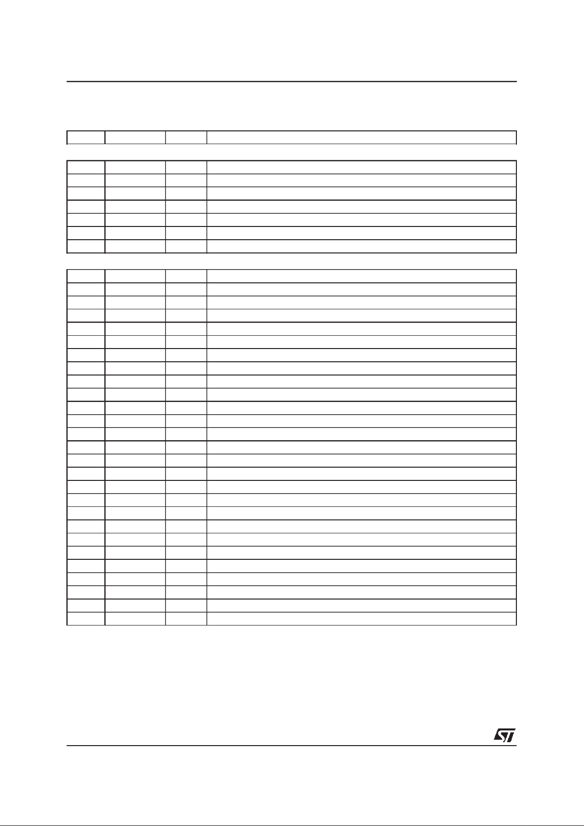
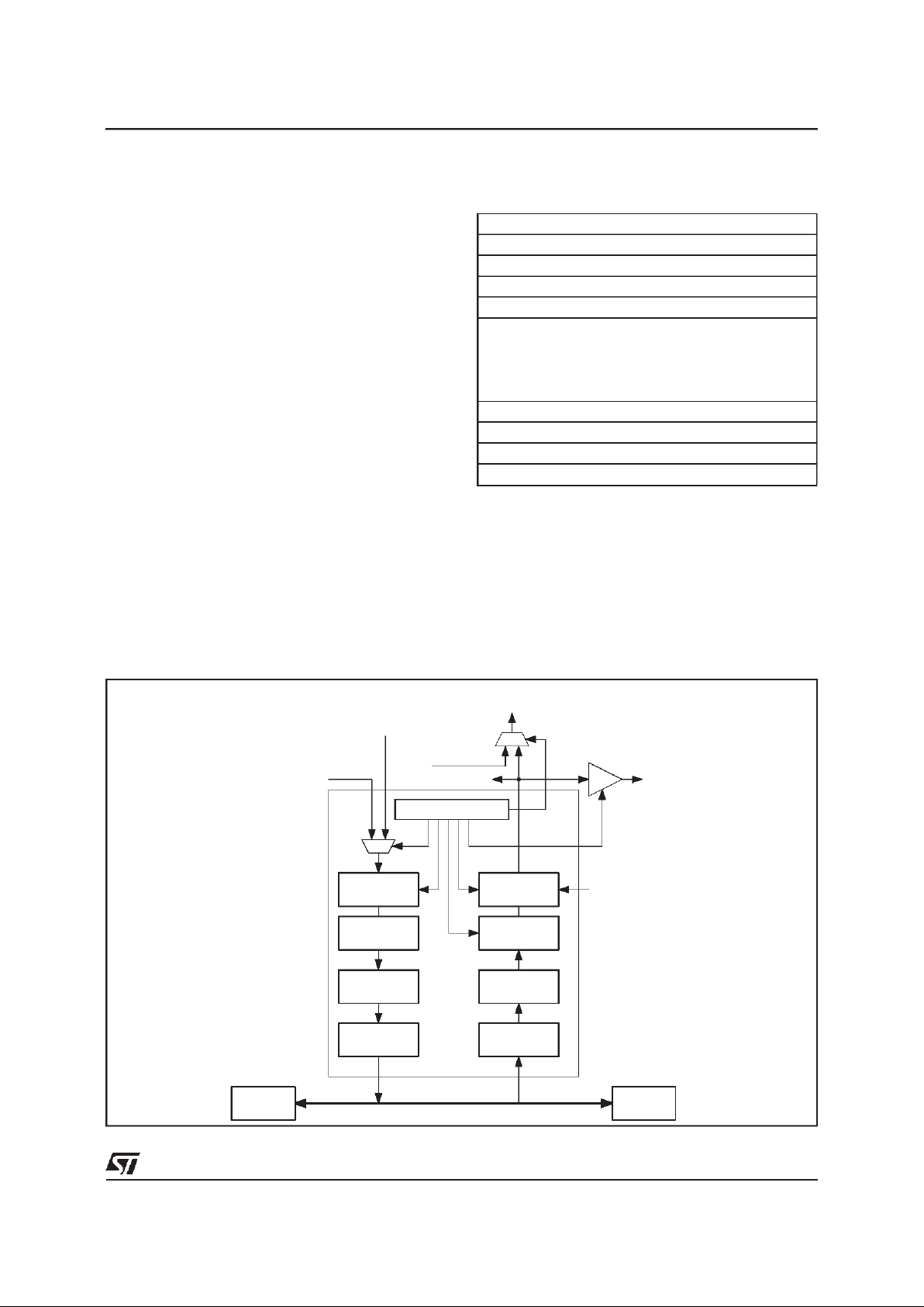
Figure1 : GeneralBlockDiagram
II - BLOCK DIAGRAM
Thetop levelfunctionalitiesof
Multi-HDLC
appearon the general block diagram.
Thereare :
- The switching matrix,
- The time slot assigner,
- The 32 HDLC transmitterswith associated DMA
controllers,
- The 32 HDLC receivers with associated DMA
controllers,
- The 16 Command/Indicateand Monitor Channel
transmitters belonging to two General Component Interfaces(GCI),
- The 16 Command/Indicateand Monitor Channel
receivers belonging to two General Component
Interfaces(GCI),
- The memory interface,
- The microprocessor interface,
- The bus arbitration,
- The clock selection and time synchronization
function,
- The interrupt controller,
- The watchdog,
- The boundaryscan.
STLC5465B
14/101
Page 15

III - FUNCTIONALDESCRIPTION
III.1- The SwitchingMatrix N x 64 KBits/S
III.1.1 - FunctionDescription
The matrix performs a non-blockingswitch of 256
time slots from 8 Input Time Division Multiplex
(TDM) at 2 Mbit/s to 8 output TimeDivision Multiplex.ATDM is composedof 32 TimeSlots (TS) at
64 kbit/s. The matrix is designed to switch a 64
kbit/s channel (Variable delay mode) or an hyperchannel of data (Sequence integrity mode). So, it
will both provide minimum throughput switching
delayfor voiceapplicationsandtimeslotsequence
integrity for data applications on a per channel
basis.
The requirements of the Sequence Integrity(n*64
kbit/s)mode are the following:
Allthe timeslotsofagiveninputframe mustbe put
out during a same output frame.
The time slots of an hyperchannel (concatenation
of TS in the same TDM) are not crossed together
at output in different frames.
In variable delay mode, the time slot is put out as
soon as possible. (The delay is two or three time
slots minimum between input and output).
For test facilities, any time slot of an Output TDM
(OTDM) can be internally looped back into the
sameInputTDM number(ITDM)at thesametime
slotnumber.
A Pseudo Random Sequence Generator and a
Pseudo Random Sequence Analyzer are implemented in the matrix.They allow the generationa
sequence on a channel or on a hyperchannel, to
analyse it and verify its integrity after several
switching in the matrix or some passing of the
sequenceacrossdifferentboards.
The Frame Signal (FS) synchronises ITDM and
OTDMbut a programmabledelayor advance can
beintroducedseparatelyon eachITDMand OTDM
(a half bit time, a bit time or two bit times).
An additional pin (PSS) permits the generationof
a programmablesignal composed of 256 bitsper
frameat a bit rate of 2048kbit/s.
An external pin (NDIS) asserts a high impedance
on all the TDM outputs of the matrix when active
(duringthe initializationof theboard for example).
III.1.2 - Architectureof the Matrix
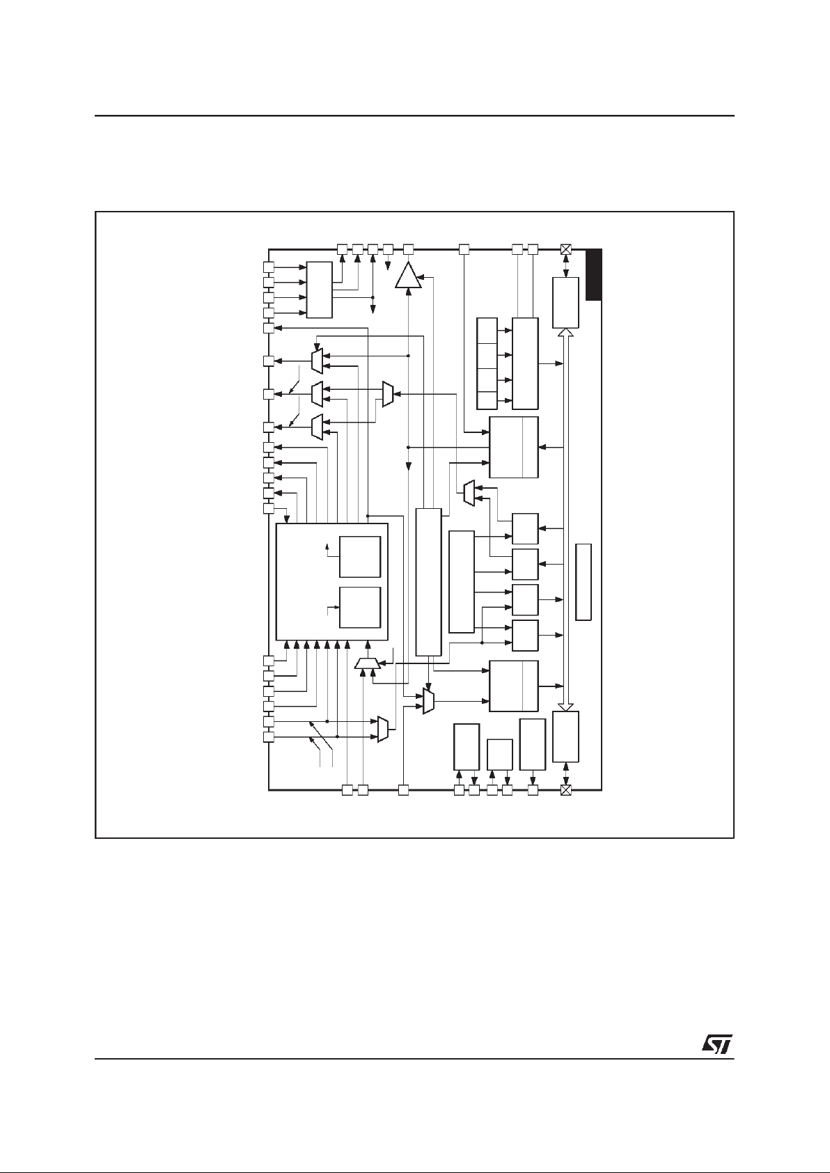
The matrix is essentially composed of bufferdata
memoriesand a connection memory.
Thereceivedserialdataisfirst convertedto parallel
byaserialtoparallelconverterandstoredconsecutively in a 256 position Buffer Data Memory (see
Figure 2 on Page 16).
To satisfy the SequenceIntegrity (n*64 kbit/s) requirements,the data memory is built with an even
memory, an odd memory and an output memory.
Twoconsecutiveframes are storedalternativelyin
theoddandevenmemory.Duringthetimeaninput
frame is stored,theone previouslystoredis transferred into the output memory according to the
connectionmemoryswitchingorders.Aframelater,
the outputmemoryis readand datais convertedto
serial and transferredto the output TDM.
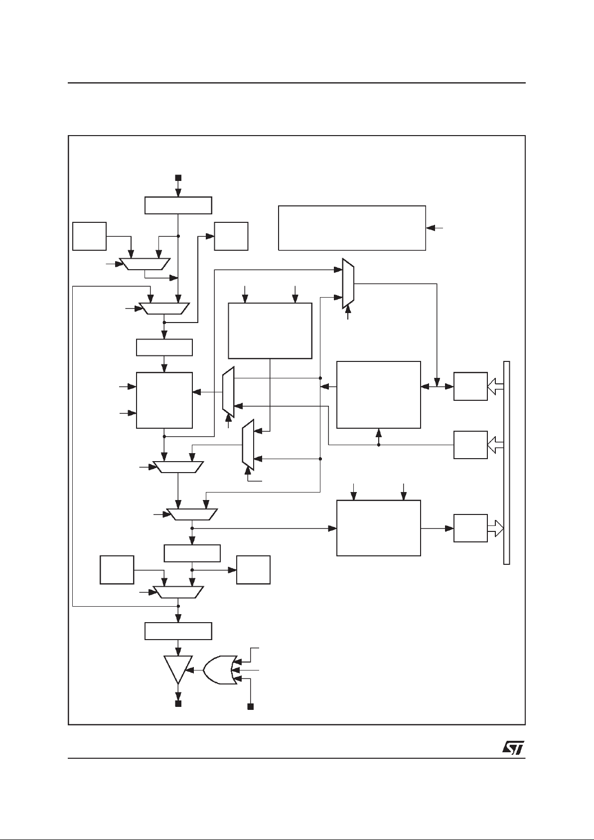
III.1.3 - Connection Function
Twotypes of connectionsare offered:
- unidirectionalconnectionand
- bidirectionalconnection.
Anunidirectionalconnectionmakesonly theswitch
ofaninputtimeslotthroughanoutputone whereas
abidirectionalconnectionestablishesthelinkin the
other directiontoo.So a doubleconnectioncan be
achieved by a single command (see Figure 3 on
Page 17).
III.1.4 - LoopBackFunction
Any time slot of an Output TDM can be internally
looped back on the time slot which has the same
TDM number and the same TS number
(OTDMi,TSj) ----> (ITDMi, TSj).
In the case of a bidirectional connection,only the
one specifiedby the microprocessoris concerned
by the loop back (see Figure 4 on Page 17).
STLC5465B
15/101
Page 16
From SMCR Register
CM
(whenRead)
LOOP
DATA
MEMORIES
64kb/s and
n x 64kb/s
CONNECTION
MEMORY
SequenceIntegrity,
LOOP, PRSA,PRSG,
INS, OTSV
Tx
HDLC
Rx
GCI
S/P
IMTD
Sequence
Integrity
INS
1
1
A
1
CM
1
PRSG
PSEUDORANDOM
SEQUENCE
GENERATOR
211-1
Rec. O.152
PRSG
SGV
PSEUDORANDOM
SEQUENCE
ANALYZER
211-1
Rec. O.152
PRSA
SAV
GCIR
BIT SYNCHRO
Tx
GCI
ME
P/S
Rx
HDLC
D4/5
D7
D0/7
1
1
D
D
D
D
A
1
CMDR
Data
Register
CMAR
Address
Register
SFCRR
SequenceFault
CounterRegister
HDLCM 1
D7 DDIINN’0/7
7
D4/5
BIT SYNCHRO
DIN 0/7
DOUT 0/7
Internal
Bus
From OMCRRegister
OMV(per multiplex)
From Connection Memory
OTSV(perchannel)
From N DIS PIN
(for all multiplexes)
PRSG :
Pseudo RandomSequenceGenerator
PRSA :
PseudoRandomSequenceAnalyzer
OTSV :
OutputTime Slot Validated
INS :
Insert
ME
: gMessa e Enable
IMTD : IncreasedMin ThroughtputDelay
SGV : SequenceGenerator Validated
SAV :
SequenceAnalyzer Validated
CM : Connection Memory(from CMARRegister)
OR
Figure2 : Switching Matrix Data Path
III - FUNCTIONALDESCRIPTION (continued)
STLC5465B
16/101
Page 17
OTSy, OTDMq
DATA
MEMORY
n x 64kb/s
DATA
MEMORY
n x 64kb/s
DOWN STREAM
ITSy, ITDMq
UP STREAM
ITSx,ITDMp
DOWN STREAM
OTSx, OTDMp
UP STREAM
Bidirectional Connection
OTSy, OTDMq
DATA
MEMORY
n x 64kb/s
DOWN STREAM
ITSx,ITDMp
DOWN STREAM
Unidirectional Connection
p, q = 0 to 7
x, y= 0 to 31
5464-04.EPS
Figure3 : Unidirectionaland BidirectionalConnections
OTSy, OTDMq
DATA
MEMORY
n x 64kb/s
DATA
MEMORY
n x 64kb/s
DOWN STREAM
ITSy, ITDMq
UP STREAM
ITSx,ITDMp
DOWN STREAM
OTSx, OTDMp
UP STREAM
OTSV
Loop
Loopback per channel relevant if bidirectional connection has been done.
p, q = 0 to 7
x, y = 0 to 31
5464-05.EPS
Figure4 : LoopBack
III - FUNCTIONALDESCRIPTION (continued)
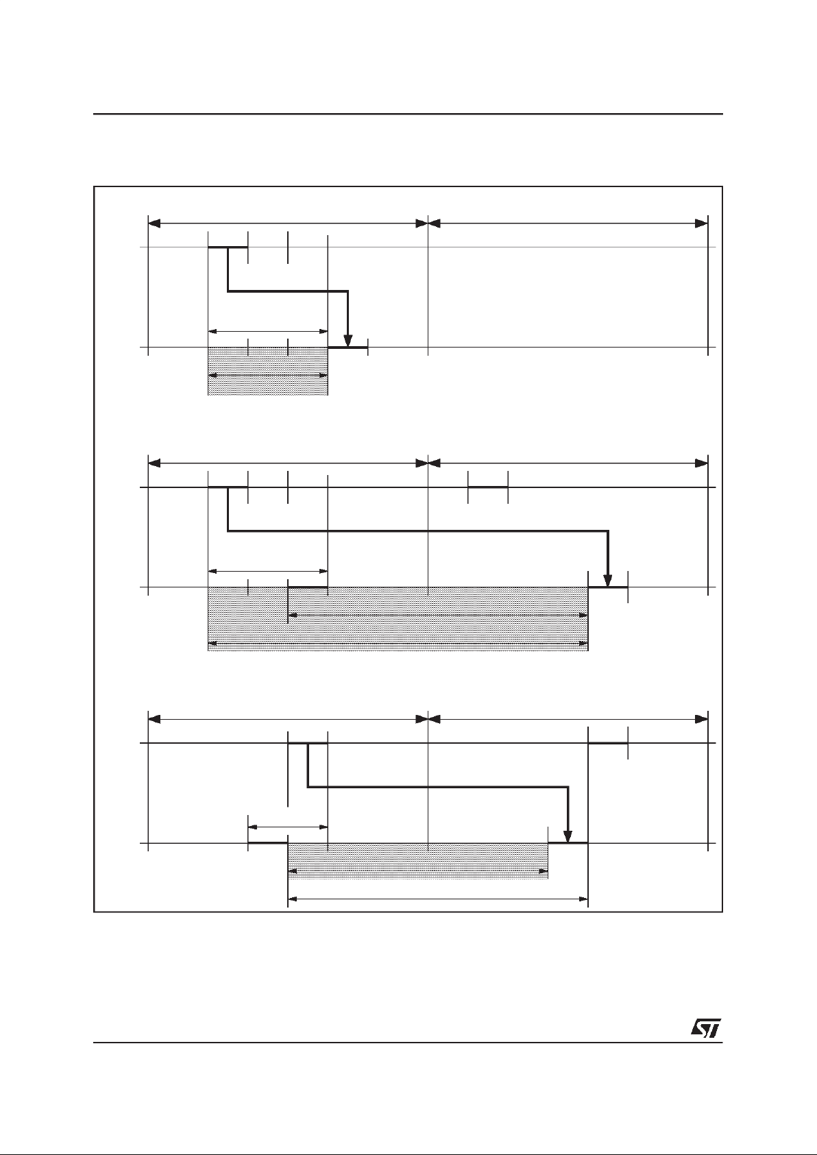
III.1.5 - Delay through the Matrix
III.1.5.1- VariableDelay Mode
In the variable delay mode, the delay through the
matrixdependson therelativepositionsof theinput
and output time slots in the frame.
So,some limitsare fixed :
- the maximumdelay isa frame+ 2 time slots,
- the minimum delay is programmable.
Three time slots if IMTD= 1, in this case n = 2 in
the fo rmula he reafter or two time slots if
IMTD = 0, in this case n = 1 in the sameformula
(see Paragraph ”Switching Matrix Configuration
Reg SMCR(0C)H” on Page 64).
Allthe possibilitiescanbe ranked in three cases :
a) If OTSy > ITSx + n then thevariabledelay is :
OTSy- ITSx Timeslots
b) IfITSx< OTSy< ITSx+nthenthevariabledelay
is :
OTSy - ITSx + 32 Timeslots
c) OTSy< ITSxthen the variable delay is :
32 - (ITSx- OTSy)Time slots.
N.B. Ruleb) and rule c) are identical.
For n = 1 and n = 2, seeFigure 5 on Page 18.
III.1.5.2- SequenceIntegrity Mode
In the sequenceintegrity mode (SI = 1, bitlocated
in theConnectionMemory),theinputtimeslotsare
putout2frameslater(fig.6-page19).Inthiscase,
the delay is definedby a single expression:
ConstantDelay = (32 - ITSx)+ 32 + OTSy
So, the delay in sequence integrity mode varies
from 33 to 95 timeslots.
STLC5465B
17/101
Page 18
Frame n Frame n + 1
ITS0 ITS31 ITS0 ITS31
OTS0 OTS31
ITSx ITSx+1 ITSx+2
OTSy
y>x+2
Variable De lay
(OTSy - ITSx)
Inpu t
Frame
Output
Frame
1) Cas e : If OTSy > ITS x + 2, then Variable Delay is : OTS y - ITSx TimeSlots
Frame n Frame n + 1
ITS0 ITS31 ITS0 ITS31
OTS0 OTS31
ITSx ITSx+1 ITSx+2
OTSy
x≤y≤x+2
32 TimeS lots
Variable De lay : OTS y - ITSx + 32 TimeSlots
Inpu t
Frame
Output
Frame
2) Cas e : If ITSx≤OTSy≤ITSx + 2, the n Variable De lay is : OTSy - ITSx + 32 TimeSlots
ITSx
OTSy
Frame n Frame n + 1
ITS0 ITS31 ITS0 ITS31
OTS0 OTS31
ITSx
OTSy
y<x
32 Tim eSlots
Variable Delay : 32 - (ITSx - OTSy) TimeS lots
Inpu t
Frame
Output
Frame
3) Cas e : If OTSy < ITS x, the n Variable De lay is : 32 - (ITSx - OTSy) TimeSlots
ITSx
OTSy
5464-06.EPS
Figure5 : VariableDelay through the matrixwith ITDM = 1
III - FUNCTIONALDESCRIPTION (continued)
STLC5465B
18/101
Page 19
Frame n Frame n + 1
ITS0 ITS31 ITS0 ITS31
OTS0 OTS31
ITSx ITSx+1 ITSx+2
OTSy
y>x+1
Variable Delay
(OTSy - ITSx)
Input
Frame
Output
Frame
1) Case : If OTSy > ITSx + 1, then Variable Delay is : OTSy - ITSx TimeSlots
Frame n Frame n + 1
ITS0 ITS31 ITS0 ITS31
OTS0 OTS31
ITSx ITSx+1 ITSx+2
OTSy
x
≤ y ≤ x+1
32 TimeSlots
Variable Delay : OTSy - ITSx + 32 TimeSlots
Input
Frame
Output
Frame
2) Case : If ITSx ≤ OTSy ≤ ITSx + 1, thenVariable Delay is : OTSy - ITSx + 32 TimeSlots
ITSx
OTSy
Frame n Frame n + 1
ITS0 ITS31 ITS0 ITS31
OTS0 OTS31
ITSx
OTSy
y<x
32 TimeSlots
Variable Delay : 32 - (ITSx - OTSy) TimeSlots
Input
Frame
Output
Frame
3) Case : If OTSy < ITSx, then Variable Delay is : 32 - (ITSx - OTSy) TimeSlots
ITSx
OTSy
5464-07.EPS
Figure6: Variable Delay throughthe matrix with ITDM = 0
III - FUNCTIONALDESCRIPTION (continued)
STLC5465B
19/101
Page 20
Cons tant Delay = (32 -ITSx) + 32 + OTSy
Framen Framen+1 Framen+2
ITS0
Min. Constant Delay = 33TS
32 Time Slots + 0 = 33
TimeSlots
Max. Constant Delay = 95 TimeSlots
32 - 0 + 32 + 31 = 95
TimeSlots
(32 - ITSx)
+32 +OTSy =Constant
Delay
ITS31 ITS0 ITS31 ITS0 ITS31
OTS0 OTS 31
1+
OTS 31
ITS :
OTS :
Input TimeSlot
Output TimeSlot
0≤x≤31
0≤y≤31
5464-08.EPS
Figure7 : Constant Delaythrough the matrixwith SI = 1
III - FUNCTIONALDESCRIPTION (continued)
STLC5465B
20/101
Page 21

III.1.6 - ConnectionMemory
III.1.6.1- Description
Theconnectionmemoryis composedof256 locations addressed by the number of OTDM and TS
(8x32).
Eachlocationpermits:
- to connecteachinputtime slotto one outputtime
slot (If two or more output time slots are connected to the same inputtime slot number,there
is broadcasting).
- to selectthe variabledelaymodeorthesequence
integritymode for anytime slot.
- to loop back an output time slot. In thiscase the
contentsof aninputtime slot(ITSx,ITDMp)is the
same as the output time slot (OTSx,OTDMp).
- to output the contents of the correspondingconnection memory instead of the data which has
been storedin data memory.
- to output the sequence of the pseudo random
sequence generator on an output time slot: a
pseudo randomsequencecan be insertedin one
or severaltime slots(hyperchannel)of the same
Output TDM ; this insertion must be enabled by
the microprocessor in the configuration register
of the matrix.
- to definethe sourceof a sequenceby thepseudo
random sequence analyzer: a pseudo random
sequence can be extracted from one or several
time slots(hyperchannel)of thesame InputTDM
and routedto the analyzer;this extractioncanbe
enabled by the microprocessorin the configuration registerof the matrix (SMCR).
- to assert a high impedance level on an output
time slot (disconnection).
- to delivera programmable256-bitsequenceduring 125microsecondsontheProgrammablesynchronizationSignal pin (PSS).
III.1.6.2- Accessto ConnectionMemory
Supposingthat the Switching Matrix Configuration
Register(SMCR) has been alreadywritten by the
microprocessor, it is possibleto access to the connectionmemoryfrommicroprocessorwiththehelp
of two registers:
- ConnectionMemoryData Register (CMDR) and
- ConnectionMemoryAddressRegister(CMAR).
III.1.6.3- Accessto Data Memory
To extract the contents of the data memory it is
possible to read the datamemoryfrom microprocessor with the help of the two registers :
- ConnectionMemoryData Register (CMDR) and
- ConnectionMemoryAddressRegister(CMAR).
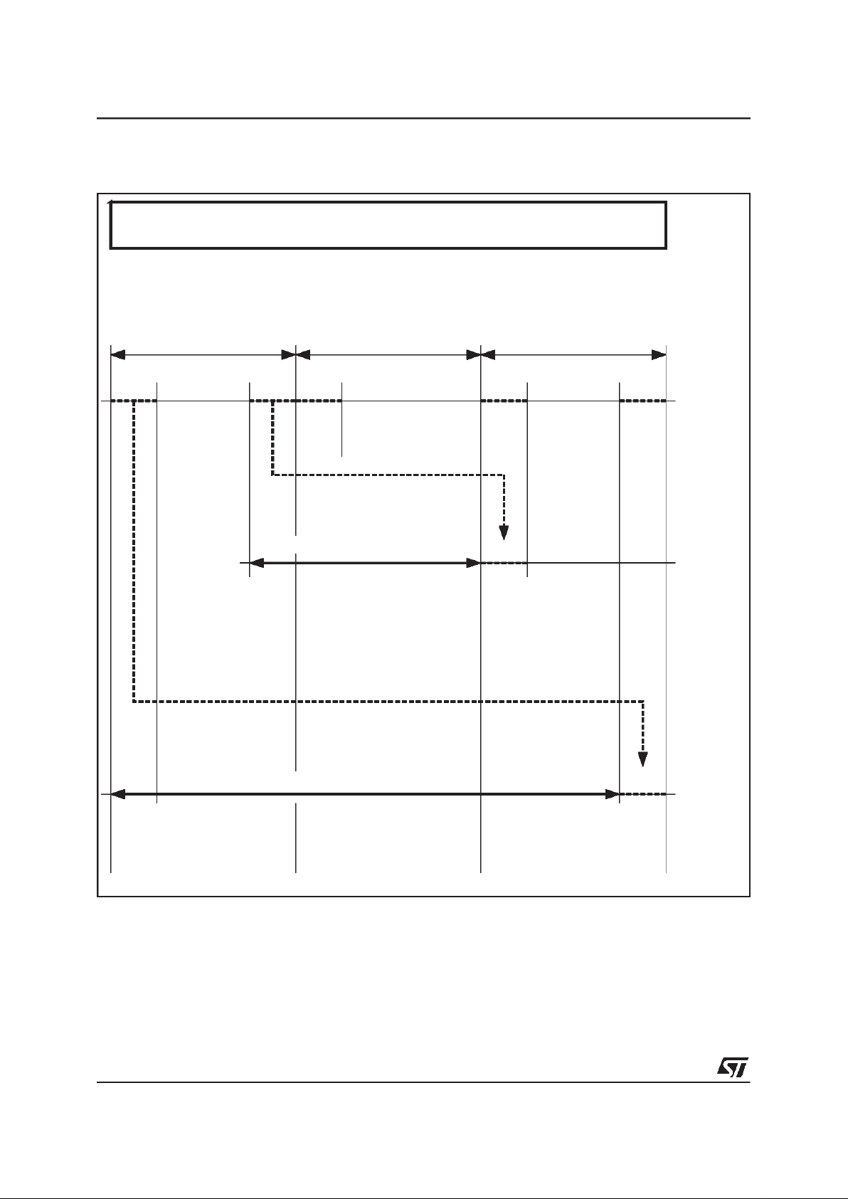
III.1.6.4- Switchingat 32 Kbit/s
Four TDMs can be programmed individually to
carry 64 channelsat 32 Kbit/s (onlyif theseTDMs
are at 2 Mbit/s).
Twobits(SW0/1)locatedin SMCR define the type
of channelsof two couples of TDMs.
SW0 defines TDM0 and TDM4 (GCI0) and SW1
defines TDM1 and TDM5 (GCI1). If TDM0 or/and
TDM1 carry 64 channels at 32 Kbit/s then TDM2
or/and TDM3 are not availableexternally theyare
used internally to perform the function.
Downstreamswitching at 32 kb/s on page 22.
Upstreamswitching at 32 kb/son page23.
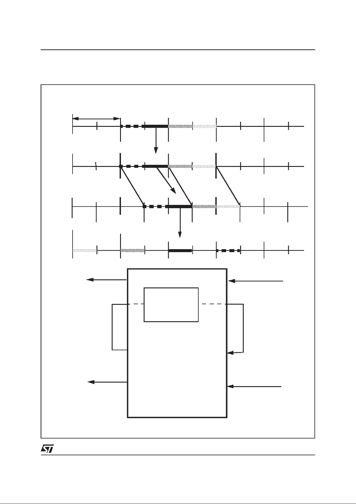
III.1.6.5- Switchingat 16 kbit/s
TheTDM4andTDM5can beGCImultipexes.Each
GCImultipexcomprises8GCIchannels.Each GCI
channelcomprisesoneD channelat 16 Kbit/s.See
GCI channeldefinition GCI Synchro signal delivered by the Multi-HDLC on page 30.
Itispossibletoswitchthecontentsof16Dchannels
from the 16 GCI channelsto 4 timeslotsof the 256
output timeslots.
In the other direction the contents of an selected
timeslot is automaticallyswitched to 4 D channels
at 16 Kbit/s.
See Connection Memory Data Register CMDR
(0E)
H
on page 74
III - FUNCTIONALDESCRIPTION (continued)
STLC5465B
21/101
Page 22

III - FUNCTIONALDESCRIPTION (continued)
dout 4 din0
dout 2 din 2
Internal
commands Switching
at 32 kb/ s
dout 5 din 1
dout 3 din 3
DIN0
din2
dout2
dout4
Internal
command
If SW0=1
DOUT4
(GCI 0)
3.9µs
a b Free c Free d Free e
abcde
ca
d b MON D C/I
dc ba
B1 B2 MON D C/I
4 bit shifting
DOUT5
DOUT4
DIN0
DIN2 notused
DIN 1
DIN3 notused
MULTI HDLC STLC546 5
SW0=1
SW1=1
4 bit shifting
(GCI 0)
(GCI 1)
DOUT2
DOUT3
D
C/I
AE
Figure8: Downstream Switching at 32kb/s
STLC5465B
22/101
Page 23
III - FUNCTIONALDESCRIPTION (continued)
DOUT 0 DIN4
DOUT6 DIN6
Switching at 32 kb/s
DOUT1 DIN5
MULTI HDLC STLC 5465
DIN4
(GCI 0)
DOUT6
DIN6 =
shifted
DOUT6
DOUT0
a
Free
b
Free
c
Free
d
Free e
dc ba
B1 B2 MON D C/I
GCI1
GCI 0
From
DOUT6
d
c
b
axyz
B2 GCI 1 B1 GCI 0 B2 GCI 0 B1 GCI 1 B2 GCI1
d
c
b
a
xy
B2 GCI1 B1 GCI0 B2 GCI 0 B1 GCI1
Timeslot (3.9µs)
Internal loopback
and
4 bit shifting (2+2)
by software
Figure9: Upstream Switching at 32kb/s
STLC5465B
23/101
Page 24
III - FUNCTIONALDESCRIPTION (continued)
TDM side
TSy ofany TDM can
be
programmablewith y
comprisedbetween
0 and 31
.
GCI side
D11
D12
D21
D22
D31
D32
D41
D42
TSy
D11
D12
C1
C2
C3
C4
A
E
D21
D22
C1
C2
C3
C4
A
E
D31
D32
C1
C2
C3
C4
A
E
D41
D42
C1
C2
C3
C4
A
E
n: GCIchannel
number, 0 to 1
TS 16n+15
TS 16n+11
TS 16n+7
TS 16n+3
Figure10: Upstream and DownstreamSwitchingat 16kb/s
STLC5465B
24/101
Page 25
TIME S LOT ASSIGNER
32 Rx HDLC
32 ADDRESS
RECOGNITION
32 Rx FIFO’s
32 Rx DMAC 32 Rx DMAC
32 Tx FIFO’s
32 Tx HDLC
32 CSMA-CR
DIN8
Direct HDLC Input
From Output 7
of the Matrix
To Input 7 of the Matrix
From Output 6
of the Matrix
DOUT 6
Direct HDLCOutput
Conte ntion
Bus
Echo
µ
P
INTERFACE
RAM
INTERFACE
5464-09.EPS
Figure11 : HDLC and DMAControllerBlockDiagram
III - FUNCTIONALDESCRIPTION (continued)
III.2- HDLC Controller
III.2.1 - FunctionDescription
The internal HDLC controller can run up to 32
channels in a conventional HDLC mode or in a
transparent (non-HDLC) mode (configurable per
channel).
Eachchannelbitrateisprogrammablefrom 4kbit/s
to64kbit/s.All the configurationsare also possible
from 32 channels (from 4 to 64 kbit/s) to one
channelat 2 Mbit/s.
Inreception,theHDLC timeslotscan directlycome
from the input TDM DIN8 (direct HDLC Input) or
from any other TDM input after switching towards
the output 7 of the matrix (configurable per time
slot).
In transmission,the HDLC frames are senton the
output DOUT6and on the outputCB (withor without contention mechanism), or are switched towards the other TDM output via the input 7 of the
matrix(see Figure 11).
III.2.1.1- Formatof the HDLC Frame
Theformatof anHDLCframeisthesameinreceive
and transmit direction and shown here after.
III.2.1.2- Compositionof an HDLC Frame
Opening Flag
Address Field (first byte)
Address Field (second byte)
Command Field (first byte)
Command Field (second byte)
Data (first byte)
Data (optional)
Data (last byte)
FCS (first byte)
FCS (second byte)
Closing Flag
- OpeningFlag
- One or twobytes for addressrecognition(reception) andinsertion (transmission)
- Data bytes with bit stuffing
- Frame Check Sequence: CRC with polynomial
G(x) = x
16+x12+x5
+1
- Closing Flag.
STLC5465B
25/101
Page 26

III.2.1.3- Descriptionand Functions of the
HDLC Bytes
- FLAG
The binarysequence01111110marksthe beginning and theend of the HDLC Frame.
Note : In reception,threepossibleflag configurations are allowed and correctlydetected:
- two normal consecutiveflags :
...0111111001111110...
- two consecutiveflags with a ”0” common:
...011111101111110...
- a global common flag : ...01111110...
this flag is the closing flag for the current frame
and the opening flag for the next frame
- ABORT
The binary sequence 1111111 marks an Abort
command.
Inreception,sevenconsecutive1’s,insidea message, are detected as an abort command and
generatesan interruptto the host.
In transmit direction, an abort is sent upon command of the micro-processor. No ending flag is
expected after the abort command.
- BIT STUFFING AND UNSTUFFING
This operation is done to avoid the confusionof
a data byte with a flag.
In transmission, if five consecutive 1’s appear in
theserialstreambeingtransmitted,a zeroisautomaticallyinserted(bit stuffing)after he fifth ”1”.
In reception,if five consecutive”1” followed by a
zero are received, the ”0” is assumed to have
been inserted and is automatically deleted (bit
unstuffing).
- FRAME CHECKSEQUENCE
TheFrameChec kSequenceiscalcu latedaccording
totherecommendationQ921oftheCCITT.
- ADDRESS RECOGNITION
In the frame, one or two bytesare transmittedto
indicate the destinationof the message.
Two types ofaddressesare possible:
- a specific destinationaddress
- a broadcast address.
In reception,thecontroller comparesthe receive
addressesto internal registers, which contain its
own address. 4 bits in the receive command
register (HRCR) inform the receiver of which
registers,it has to take into account for the comparison. The receiver can compare one or two
address bytes of the message to the specific
board address and/or the broadcastaddress.
For the specific destination address only, the
receiver can compare or not each bit of the two
receive address bytes to the programmableAddress Field Recognition register. An Address
Field RecognitionMask register is associatedto
eachAddressFieldRecognitionregister; soeach
received address bit can be masked or not individually.
TheprogrammableAddressFieldRecognitionregister is located in the Address Field Recognition
MemoryandtheprogrammableAddressFieldRecognition Mask register is located in the Address
FieldRecognitionMaskMemory.
Upon an address match, the address and the
datafollowingarewrittentothedatabuffers;upon
an address mismatch, the frame is ignored. So,
it authorizes the filtering of the messages. If no
comparison is specified, each frame is received
whateverits addressfield.
In Transmission, the whole of the transmitframe
is locatedin sharedmemory;thecontrollersends
the frame including the destination or broadcast
addresses.
III.2.2 - CSMA/CRCapability
An HDLC channelcan come in and go out by any
TDM input on the matrix. For time constraints,
direct HDLC Accessis achievedby theinputTDM
(DIN 8)and the outputTDM(DOUT6).
Intransmission, a timeslotof aTDM canbeshared
between different sources in Multi-point to point
configuration(differentsubscriber’sboardsforexample).ThearbitrationsystemistheCSMA/CR(Carrier
SenseMultipleaccesswithContention Resolution).
The contention is resolvedby a bus connectedto
the CB pin (ContentionBus).This bus is a 2Mbit/s
wire line common to all the potentialsources.
If a
Multi-HDLC
hasobtainedtheaccesstothebus,
thedatatotransmitis sentsimultaneouslyontheCB
lineandtheoutputTDM.Theresultofthe contention
isreadbackontheEcholine.Ifacollisionisdetected,
the transmission is stoppedimmediately. A contentionona bitbasisissoachieved. Each message to
be sentwith CSMA/CRhasa priorityclass(PRI= 8,
10) indicatedby theTransmit Descriptor and some
rulesare implementedtoarbitratethe accessto the
line. The CSMA/CR Algorithm is given. When a requestto send a message occurs, the transmitter
determines if thesharedchannelis free.The
Multi-
HDLC
listenstotheEcholine.IfCormoreconsecutive
”1” are detected (C depending on the message’ s
priority),the
Multi-HDLC
beginstosendits message.
Eachbitsent issampledbackandcomparedwith the
originalvaluetosend.Ifabitisdifferent,thetransmissionisinstantaneous l ystopped(beforethe endofthis
bittime)andwill restartassoonasthe
Multi-HDLC
will
detectthatthechannel is freewithoutinterruptingthe
micropr oc essor.
After a successful transmission of a message, a
III - FUNCTIONALDESCRIPTION (continued)
STLC5465B
26/101
Page 27

programmablepenaltyPEN(1or2) isappliedto the
transmitter(see Paragraph HDLC Transmit CommandRegister on Page 81). It guaranteesthat the
same transmitterwill not takethebusanothertime
beforea transmitterwhich has to send a message
of same priority.
In case of a collision, the frame which has been
abortedis automaticallyretransmittedby the DMA
controller without warning the microprocessor of
this collision. The frame can be located in several
buffers in external memory. The collision can be
detectedfromthe secondbit of the openingframe
to the last but one bit of the closingframe.
III.2.3 - TimeSlot Assigner Memory
Each HDLC channel is bidirectional and configurateby theTime Slot Assigner(TSA).
TheTSAis amemoryof32words(oneper physical
TimeSlot)where all ofthe 32 inputand outputtime
slots of the HDLC controllers can be associated
to logical HDLC channels. Super channels are
created by assigning the same logical channel
numberto severalphysicaltime slots.
The following features are configurate for each
HDLC time slot :
- Time slot used or not
- One logicalchannel number
- Its source : (DIN8 or the output7 of the matrix)
- Its bit rate and concerned bits (4kbit/s to
64kbit/s). 4kbit/s correspond to one bit transmitted each two frames. This bit mustbe presentin
two consecutive frames in reception, and repeated twice in transmission.
- Its destination:
- direct output on DOUT6
- direct output on DOUT6 and on the Contention
Bus(CB)
- on another OTDM via input7 of the matrix and
on the ContentionBus (CB)
III.2.4 - Data StorageStructure
Dataassociatedwitheach Rx andTxHDLCchannelis storedin externalmemory;Thedatatransfers
between the HDLC controllers and memory are
ensuredby32 DMAC(DirectMemoryAccessController)in reception and 32 DMAC in transmission.
The storage structure chosen in both directionsis
composed of one circular queue of buffers per
channel. In such a queue, each data buffer is
pointedto bya Descriptorlocatedinexternalmemory too. The main information contained in the
Descriptor is the address of the Data Buffer, its
length and the address of the next Descriptor; so
the descriptors can belinked together.
This structure allows to :
- Store receive frames of variable and unknown
length
- Read transmitframes storedin externalmemory
by the host
- Easily performthe frame relay function.
III.2.4.1- Reception
At the initializationof the application, the host has
to prepare an Initialization Block memory, which
containsthe first receivebuffer descriptoraddress
for each channel, and the receivecircularqueues.
At the opening of a receive channel, the DMA
controller reads the address of the first buffer descriptorcorrespondingto thischannelintheinitialization Block. Then, the data transfer can occur
without intervention of the processor (see Figure
12 on Page 28).
Anew HDLCframe alwaysbeginsin a new buffer.
A long frame can be split between several buffers
if the buffersizeis not sufficient.All theinformation
concerning the frame and its location in the
circular queue is included in the Receive Buffer
Descriptor:
- The Receive Buffer Address(RBA),
- The size of thereceive buffer (SOB),
- Thenumberof byteswritteninto thebuffer(NBR),
- The Next Receive DescriptorAddress(NRDA),
- The status concerningthe receiveframe,
- The control of the queue.
III.2.4.2- Transmission
In transmission, the data is managed by a similar
structure as in reception (see Figure 13 on
Page 28).
By the same way, a framecan be splitup between
consecutivetransmit buffers.
The main information contained in the Transmit
Descriptorare :
- transmitbufferaddress (TBA),
- numberof bytesto transmit(NBT)concerningthe
buffer,
- next transmit descriptoraddress (NTDA),
- statusof the frame after transmission,
- control bit of the queue,
- CSMA/CR priority(8 or 10).
III.2.4.3- Frame Relay
The principle of the frame relay is to transmit a
frame which has been received withouttreatment.
A new heading is just added. This will be easily
achieved,takingintoaccount that the queue structure allows the transmission of a frame split between several buffers.
III - FUNCTIONALDESCRIPTION (continued)
STLC5465B
27/101
Page 28
RECEIVE
DMA
CONTROLLER
RDA0
RDA1
Initialization Block
up to32 channels
RDA31
Receive
Buffer n
Receive
Descriptorn
NRDA
RBA
Receive
Buffer 2
NRDA
RBA
Receive
Descriptor 2
Receive
Buffer 1
NRDA
RBA
Initial Receive
Descriptor
Receive
Buffer 3
Receive
Descriptor3
NRDA
RBA
One receivecircular queue by channel
5464-10.EPS
Figure12 : Structureof the ReceiveCircular Queue
III - FUNCTIONALDESCRIPTION (continued)
TRANSMIT
DMA
CONTROLLER
TDA0
TDA1
Initialization Block
up to32 channels
TDA31
Transmit
Buffer n
Transmit
Descriptor n
NTDA
TBA
Transmit
Buffer 2
NTDA
TBA
Transmit
Descriptor 2
Transmit
Buffer 1
NTDA
TBA
Initial Transmit
Descriptor
Transmit
Buffer 3
Transmit
Descriptor3
NTDA
TBA
One transmitcircular queue by channel
5464-11.EPS
Figure13 : Structureof the TransmitCircular Queue
STLC5465B
28/101
Page 29

III.2.5 - Transparent Modes
Inthetransparentmode,the
Multi-HDLC
transmits
data in a completely transparent manner without
performingany bit manipulation or Flag insertion.
Thetransparentmodeis per bytefunction.
Two transparentmodes are offered:
- First mode : for the receive channels, the
Multi-HDLC
continuously writes received bytes
into theexternal memory as specifiedin thecurrentreceivedescriptorwithouttakingintoaccount
the Fill CharacterRegister.
- Secondmode:theFil lCharacterRegister specifies
the”fil lcharac ter”whichmustbe takenintoaccount.
Inreception,the”fillcharacter”willnotbetransferred
totheexternalmemory.Thedetectionof”Fillcharacter”marks the end of a messageand generatesan
interruptifBINT=1(seeTransmitDescriptoronPage
95).Whenthe”Fill character”is not detecteda new
messageisreceiving.
As for the HDLC mode the correspondence
between the physical time slot and the logical
channel is fully defined in the Time Slot Assigner
memory(Time slot usedor notused,logicalchannel number,source,destination).
III.2.6 - Commandof the HDLC Channels
The microprocessoris able to control each HDLC
receive and transmit channel. Some of the commands are specific to the transmission or the receptionbut others are identical.
III.2.6.1- ReceptionControl
Theconfigurationof the controlleroperatingmode
is: HDLC mode or Transparentmode.
The control of the controller: START, HALT,CONTINUE,ABORT.
- START: On a start command, the RxDMA controller reads the address of the first descriptor in
the initialization block memory and is ready to
receive a frame.
- HALT: For overloading reasons,themicroprocessor can decideto halt the reception.TheDMA
controllerfinishestransferof the currentframeto
externalmemory and stops. The channel can be
restartedon CONTINUEcommand.
- CONTINUE : The reception restarts in the next
descriptor.
- ABORT:On an abortcommand, the reception is
instantaneously stopped. The channel can be
restartedon a STARTor CONTINUEcommand.
Receptionof FLAG(01111110) or IDLE (11111111)
betweenFrames.
Address recognition. The microprocessordefines
theaddressesthattheRx controllerhastotakeinto
account.
In transparent mode: ”fill character” register selected or not.
III.2.6.2- TransmissionControl
The configurationof the controlleroperatingmode
is : HDLC mode or Transparentmode.
The control of the controller: START, HALT,CONTINUE,ABORT.
- START:Ona startcommand,theTxDMAcontroller reads the address of the firstdescriptor in the
initializationblockmemoryandtries to transmitthe
firstframe if End Of Queueisnotat”1”.
- HALT : The transmitter finishes to sendthe currentframeandstops.Thechannel can be restarted on a CONTINUE command.
- CONTINUE : iftheCONTINUEcommand occurs
after HALTcommand,the HDLC Transmitter restarts by transmittingthe next buffer associated
to the next descriptor.
If the CONTINUE command occurs after an
ABORT command which has occurred during a
frame,theHDLC transmitterrestartsby transmittingthe framewhichhasbeeneffectivelyaborted
by the microprocessor.
- ABORT:On an abortcommand,thetransmission
of the current frame is instantaneouslystopped,
an ABORTsequence”1111111” is sent, followed
by IDLE or FLAG bytes. The channel can be
restartedon a START or CONTINUEcommand.
Transmission of FLAG (01111110) or IDLE
(111111111)betweenframes can be selected.
CRC can be generated or not. If the CRC is not
generated by the HDLC Controller, it must be located in the shared memory.
In transparentmode: ”fillcharacter”registercanbe
selectedor not.
III.3 - C/I and Monitor
III.3.1 - FunctionDescription
The
Multi-HDLC
is abletooperateboth GCIandV*
links. The TDM DIN/DOUT 4 and 5 are internally
connected to the CI and Monitor receivers/transmitters.Sincethecontrollershandleupto 16CIand
16 Monitor channels simultaneously, the
Multi-
HDLC
can manage upto 16 level1 circuits.
The
Multi-HDLC
canbeusedto supporttheCI and
monitor channels based on the following protocols :
- ISDN V* protocol
- ISDN GCI protocol
- Analog GCI protocol.
III - FUNCTIONALDESCRIPTION (continued)
STLC5465B
29/101
Page 30
III.3.2 - GCIand V*Protocol
ATDM can carry8 GCI channels or V* channels. The monitor and S/C bytes always stand at the same
positionin the TDM in both cases.
Channel 0
Channel 1 to Channel 30
Channel 31
TS0 TS1 TS2 TS3 TS28 TS29 TS30 TS31
B1 B2 MON S/C B1 B2 MON S/C
III - FUNCTIONALDESCRIPTION (continued)
The GCI or V* channelsare composedof 4 bytes
and have both the samegeneral structure.
B1 B2 MON S/C
B1,B2 : Bytes of data. Those bytes are not
affectedby themonitorand CIprotocols.
MON : Monitor channel for operation and
maintenanceinformation.
S/C : Signallingand controlinformation.
Only Monitor handshakes and S/C bytes are dif-
ferentin the threeprotocols:
ISDN V* S/C byte
D C/I 4 bits T E
ISDN GCI S/C byte
D C/I 4 bits A E
AnalogGCIS/C byte
C/I 6 bits A E
CI : The Command/Indicate channel is used for
activation/deactivation of lines and control
functions.
D : These 2 bits carry the 16 kbit/s ISDN basic
accessD channel.
In GCI protocol, A and E are the handshake bits
and are used to controlthe transfer of information
on monitor channels.TheE bit indicates the transfer of each new byte in one directionand the Abit
acknowledgesthis byte transfer in the reverse direction.
InV*protocol,thereisn’t anyhandshakemode.The
transmitter has only to mark the validity of the
Monitorbyte by positioningtheE bit (Tis not used
and is forcedto ”1”).
For more information about the GCI and V*, refer
to the General Interface Circuit Specification (issue1.0, march 1989) and the France Telecom
Specification about ISDN Basic Access second
generation(November 1990).
III.3.3 - Structure of the Treatment
GCI/V* TDM’s are connected to DIN 4 and DIN 5.
The D channels are switched through the matrix
towards the output 7 and the HDLC receiver. The
Monitorand S/C bytesare multiplexedand sent to
the CI and Monitor receivers (see Figure 14 on
Page 31).
In transmission, the S/C and Monitor bytes are
recombined by multiplexing the information providedbytheMonitor,C/IandtheHDLCTransmitter.
Likeinreception,theDchannelisswitchedthrough
the matrix.
III.3.4 - CIand Monitor Channel Configuration
Monitorchannel data is located in a timeslot ; the
CI and monitorhandshakebits arein the next time
slot.
Each channel can be defined independently. A
table with all the possible configurations is presentedhereafter (Table 13).
Table13 : C/I and MON Channel Configuration
C/I validated or not
CI For analog subscriber (6 bits)
CI For ISDN subscriber (4 bits)
Monitor validated
or not
Monitor V*
Monitor GCI
Note : A mix of V* and GCI monitoring can be performed for two
distinct channels in the same application.
III.3.5- CI and Monitor Transmission/Reception
Command
The reception of C/I and Monitor messages are
managedby two interrupt queues.
In transmission, a transmit command register is
implementedforeach C/Iand monitorchannel (16
C/I transmit command registers and 16 Monitor
transmit command registers). Those registers are
accessible in read and write modes by the microprocessor.
STLC5465B
30/101
Page 31

III - FUNCTIONALDESCRIPTION (continued)
16 Rx
C/I
16 Rx
MON
16 Tx
C/I
16 Tx
MON
INTERRUPT
CONTROLLER
GCI CHANNEL DEFINITION
DIN5 DIN 4 DOUT 4 DOUT 5
SWITCHING
MATRIX
1
2
0
3
4
5
6
7
1
2
0
3
4
5
6
7
D Cha nne ls
to Rx HDLC
DChannels
from Tx HDLC
Internal Bus
GCI1 G C I0 GCI1GCI0
5464-12.EPS
Figure14 : D, C/I and Monitor ChannelPath
III.3.6- Scramblerand Descrambler
TheTDM4andTDM5canbeGCImultipexes.Each
GCImultipexcomprises8GCIchannels.EachGCI
channelcomprisestwo B channels at 64 Kbit/s.
Inreceptionit is possibletoswitchand to scramble
the contentsof 32 B channels of GCI channels to
32 timeslots of the 256 output timeslots. In transmission these 32 timeslots are assigned to 32 B
channels.
Inthe other direction the contentsof an selectedB
channels is automatically switched and descrambled to one B channel of 16 GCI channel.
See Connection Memory Data Register CMDR
(0E)Hon page 74 (SCRbit).
Connection between “ISDN channels” and GCI
channels.
Three timeslots are assigned to one“ISDN channels”. Each “ISDN channels” comprises three
channels:B1+B2+B*with B*=D1,D2, A,E, S1,S2,
S3, S4. GCI channel to/from ISDN channel on
page32.
Upstream. From GCI channelsto ISDN channels
on page 33.
- in reception: 16 GCI channels (B1+B2+MON+
D+C/I),
- in transmission:16 ISDN channels (B1+B2+B*).
It ispossibleto switchthecontentsof B1, B2 and
D channelsfrom16 GCIchannelsinany16 “ISDN
channels”,TDM side.
The contents of B1 and/or B2 can be scrambled
ornot.If scrambledthenumberofthe32timeslots
(TDM side) are different mandatory.
Receivingthecontentsof MonitorandCommand
/ Indicatechannelsfrom16 GCI channels.Primitives and messages are stored automatically in
the externalshared memory.
Transmitting“sixbit word” (A, E, S1, S2, S3,S4)
to any 16 “ISDNchannels”TDMside or not. See
SBV bitof General Configuration Register GCR
(02)H on page 68.
Downstream. From ISDN channels to GCI channels on page 34.
- in reception: ISDN channel (B1+B2+B*)
- in transmission: GCI channel (B1+B2+MON+
D+C/I)
It ispossibleto switchthecontentsof B1, B2 and
D channelsfrom 16 “ISDN channels”, TDM side
STLC5465B
31/101
Page 32

in 16 GCIchannels.
The contents of B1 and/or B2 can be descrambled or not. If descrambledthe 32 B1/B2 belong
to GCI channelsmandatory.
Receivingsixbitword(A,E,S1,S2, S3,S4)from
any 16 “ISDN channels”, TDM side. The 16 “six
bit word” are stored automaticallyin the external
shared memory.
Transmitting the contents of Monitor and Command / Indicate channels to 16 GCI channels.
See SBV bit of General Configuration Register
GCR (02)H on page68.
AlarmIndication Signal.
This detection concerns 16 hyperchannels. One
hyperchannelcomprises16 bits (B1 and B2 only).
TheAlarmIndicationsforthe16hyperchannelsare
stored automatically in the external shared memory.SeeAISDbitof SwitchingMatrixConfiguration
Reg SMCR(0C)Hon page 71.
TDM side
PCM at 2 Mb/s
m: ISDN channel
number,0 to 9
If TDMat 4 Mb/s
odd timeslot
or eventimeslot
can be selected
GCI side
n: GCI channel
number,0 to 7
SCRAMBLER/
DESCRAMBLER
SCRAMBLER/
DESCRAMBLER
Six bit word Primitive
CommandIndicate controllers
RX TX
Monitorcontrollers
TX RX
C/I interrupt
Queue located in
shared memory
Microprocessor
MON interrupt
Queue located in
shared memory
B1
B1
B1
B1
B1
B1
B1
B1
B1
B2
B2
B2
B2
B2
B2
B2
B2
M1
M2
M3
M4
M5
M6
M7
M8
D
D
C1
C2
C3
C4
A
E
TS4n+3
TS4n+2
TS4n+1
TS4n
B1
B1
B1
B1
B1
B1
B1
B1
B1
B2
B2
B2
B2
B2
B2
B2
B2
TS3m+1
TS3m
D
D
A
E
S1
S2
S3
S4
TS3m+2
Figure15: GCI channelto/from ISDN Channel
III - FUNCTIONALDESCRIPTION (continued)
STLC5465B
32/101
Page 33

III - FUNCTIONALDESCRIPTION (continued)
TDM 0, 2
if PCM
at 4 Mb/s
GCI side
DIN4/5
SCRAMBLER
up to 32
SWITCHING
MATRIX
RX MON
controllers
up to 16
C/I interrupt Queue,
MONinterruptQueue,
locatedin shared memory
Microprocessor
RX C/I
controllers
up to 16 for
primitives
Interruptcontroller
ExtensionTX
C/Icontrollers
up to16 for
A,E, S1 to S4
SBV
1
SCR
D,A, E S1 to S4
B1, B2
bytimeslot
for the 16
controllers
Figure16: From GCI Channelsto ISDN Channels
STLC5465B
33/101
Page 34

III.4- MicroprocessorInterface
III.4.1 - Description
The
Multi-HDLC
circuitcanbecontrolledbyseveral
typesof microprocessors(ST9, Intel/Motorola8or
16 data bits interfaces) such as :
- ST9 family
- INTEL 80C1888 bits
- INTEL 80C18616 bits
- MOTOROLA6800016 bits
- MOTOROLA6802016/32 bits
- ST10 family
During the initialization of the
Multi-HDLC
circuit,
themicroprocessorinterfaceisinformedof thetype
ofmicroprocessorthatis connectedby polarisation
of three externalpinsMOD 0/2).
TwochipSelect(CS0/1)pinsareprovided.CS0will
select the internalregisters and CS1 the external
memory.
Table14 : MicroprocessorInterface Selection
MOD2
Pin
MOD1
Pin
MOD0
Pin
Microprocessor
0 1 1 80C188
1 1 1 80C186
1 0 0 68000
0 0 0 68020
001 ST9
1 0 1 ST10 A/D multiplexed
1 1 0 ST10 A/D not multiplexed
0 1 0 Reserved
TDM 0, 2
if PCM
at 4 Mb/ s
GCI side
DOUT4/5
DESCRAMBLER
up to 32
SWITCHING
MATRIX
TX MON
controller
up to 16
primitives
C/I interrupt Queue
locatedin sharedmemory
Microprocessor
AIS
Detection
up to 16
ISDN channels
Interrupt controller
TX C/I
controller
up to 16
primitives
SCR
A,E, S1 to S4
B1, B2
by timeslot
ExtensionRX
C/I controller
up to 16
ISDN channels
B1, B2
D
A, E,MONC/I
B1, B2
(16 bits)
Figure17: From ISDN channelsto GCI Channels
III - FUNCTIONALDESCRIPTION (continued)
STLC5465B
34/101
Page 35

III.4.2 - Exchangewith the sharedmemory
AFetchBufferlocatedin the microprocessorinterface allows to reduce the shared memory access
cyclefor the microprocessor.
Itisusedwhatevermicroprocessorselectedthanks
to MOD0/2 pins.
This Fetch Buffer consists of one Write FIFO and
fourRead Fetch Memories.
III.4.2.1- WriteFIFO
When the microprocessor delivers the address
word named An to write data named [An] in the
shared memory in fact it writes data [An] and
addresswordAnintheWriteFIFO(Deep 4 words).
If An is in FetchMemory, [An] is removedin Fetch
Memory.
The number of wait cycles for the microprocessor
is strongly reduced.
III.4.2.2- Read Fetch Memory
When the microprocessor delivers the address
wordnamedAnto readdatanamed[An]outofthe
shared memoryin factit reads data [An] from one
of four ReadFetch Memories.
Thenumberofwait cycle for the microprocessoris
strongly reduced and can reach zero when An,
addressworddeliveredbythemicroprocessor,and
data[An] isalreadyin theReadFetchMemory and
validated.
The source of [An] is truly the shared memory
whateverAn.
III.4.3 - Definitionof the Interfacefor the different microprocessors
Thesignalsconnectedtothemicroprocessorinterface are presented on the following figures for the
differentmicroprocessor.
Shared memory
To shared memory From shared memory
Write FIFO An, [An]
microprocessor
interface
Read Fetch
Memory
Four
Fetch Memories
An, [An]
An+1, [An+1]
An+2, [An+2]
An+3, [An+3]
From microprocessor To microprocessor
Microprocessor
Figure17.1: Write FIFO and FetchMemories.
STLC5465B
35/101
Page 36

III - FUNCTIONALDESCRIPTION (continued)
µPST9/10
INTEL
MOTOROLA
8/16 BITS
MULTI-HDLC
Internal Bus
BUSARBITRATION
µ
P
INTERFACE
Multiplex
Address/Data Bus
Address Bus
Data Bus
RAM
INTERFACE
STATIC or
DYNAMIC RAM
(organized
by 16 bits)
Figure18 :
Multi-HDLC
connectedto µP with multiplexed buses
MULTI-HDLC
Internal Bus
BUS ARBITRATION
Address Bus
DataBus
RAM
INTERFACE
STATICor
DYNAMIC RAM
(organized
by16 bits)
µPST10
INTEL
MOTOROLA
8/16 BITS
µP
INTERFACE
AddressBus
Data Bus
Figure19 :
Multi-HDLC
connectedto µP with non-multiplexedbuses
INT0/1 WDO
NRESET
CS0/1
ARDY
NWR
NRD
ALE
A8/19
AD0/7
INTEL
80C188
µ
P
INTERFACE
5464-15.EPS
Figure20 : MicroprocessorInterface for INTEL80C188
INT0/1 WDO
NRESET
CS0/1
ARDY
NWR
NRD
ALE
A16/19
AD0/15
INTEL
80C186
µ
P
INTERFACE
NBHE
5464-16.EPS
Figure21 : MicroprocessorInterface for INTEL80C186
STLC5465B
36/101
Page 37

III - FUNCTIONALDESCRIPTION (continued)
INT0/1 WDO
NRESET
CS0/1
R/NW
NUDS
NLDS
NAS
A1/23
AD0/7
MOTOROLA
68000
µ
P
INTERFACE
NDTACK
MHDLC
R/NW
CS0/1, Ax/23
AD8/15
5464-15.EPS
Figure22 : MicroprocessorInterface for MOTOROLA68000
INT0/1 WDO
NRESET
CS0/1
WAIT
R/NW
NDS
NAS
A8/15
AD0/7
ST9
µP
INTERFACE
MHDLC
5464-19.EPS
Figure24 : MicroprocessorInterface for ST9
INT0/1 WDO
NRESET
CS0/1
SIZE0/1
R/NW
NDS
NAS
A0/23
MOTOROLA
680200
µ
P
INTERFACE
NDSACK0/1
AD0/7
R/NW
CS0/1, Ax/23
AD8/15
MHDLC
Figure23 : MicroprocessorInterface for MOTOROLA68020
STLC5465B
37/101
Page 38

III.5- MemoryInterface
III.5.1 - FunctionDescription
The memory interface allows the connection of
Static or Dynamic RAM. The memory space addressablein thetwo configurationsisnotthesame.
Inthecaseof dynamicmemory(DRAM),the memory interface will address up to 16 Megabytes. In
caseof staticmemory(SRAM)only1 Megabytewill
be addressed. The memory location is alwaysorganizedin 16 bits.
The memory is shared between the
Multi-HDLC
andthe microprocessor.Theaccesstothememory
is arbitrated by an internal function of the circuit:
the bus arbitration.
III.5.2 - Choice of memory versusmicroprocessorand capacityrequired
The memory interface depends on the memory
chips which are connected. As the memory chips
will be chosen versus the microprocessor and the
wanted memory space, the following table presents the different configurations DRAM and
SRAMselectionversusµP.
Example1 : iftheapplicationrequires 16bitmProcessorand1MegawordSharedmemorysize, three
capabilitiesare offered:
- 4 DRAMCircuits (256Kx16) or
- 4 DRAMCircuits (1Mx4) or
- 1 DRAMCircuit (1Mx16).
Example2 :if theapplicationrequires8 bit mProc-
essorand 1 MegabyteSharedmemorysize,three
capabilitiesare offered:
- 2 DRAMCircuits (256Kx16) or
- 8 SRAMCircuits (128Kx8)or
- 2 SRAMCircuits (512kx8).
Example3 : for small applicationsit ispossible to
connect 2 SRAM Circuits (128Kx8) to obtain 256
Kilobytesshared memory.
III.5.3 - MemoryCycle
For SRAM and DRAM, the different cycles are
programmable. See Memory Interface Configuration Regist. MICR (32)
H
on Page 88.
Each cycle is equal to : p x 1/f
with f the frequencyof signalappliedto theCrystal
1 inputand p selected by the user.See page 9.
III - FUNCTIONALDESCRIPTION (continued)
Table 22 : DRAM and SDRAM Selection versus µP
Microprocessor and
shared memory
Shared memory size required by the application
8 bits
µProcessor
Number of
Megabytes
0.5 1 2 4 8 16
16/32 bits
µProcessor
Number of
Megawords
0.25 0.5 1 2 4 8
DRAM Circuits proposed
Capacity Organization
4 Megabits 256Kx16 1(256Kx16) 2(256Kx16) 4(256Kx16)
1Mx4 4(1Mx4) 8(1Mx4) 16(1Mx4)
16 Megabits 1Mx16 1(1Mx16) 2(1Mx16) 4(1Mx16)
4Mx4 4(4Mx4) 8(4Mx4)
64 Megabits 4Mx16 1(4Mx16) 2(4Mx16)
SRAM Circuits proposed
Not possible
Capacity Organization
1 Megabits 128Kx8 4(128Kx8) 8(128Kx8)
4 Megabits 512kx8 2(512kx8)
STLC5465B
38/101
Page 39

III - FUNCTIONALDESCRIPTION (continued)
7
N
ADM0/16, NWE,NOE
are connectedto eachcircuit
CE7
5
NCE5
1
NCE1
3
NCE3
6
NCE6
4
NCE4
0
NCE0
2
NCE2
DM8/15 DM0/7
128Kx 16
128K x 8 circuit
Figure25 :n x128K x 16 SRAMMemory
Organization
7
RAS3
5
RAS2
1
RAS0
3
RAS1
6
4
0
2
DM8/15 DM0/7
256K x 16
CAS1 CAS0
ADM0/8, NWE, NOE are connected to each circuit.
5464-22.EPS
Figure 27 : 256Kx 16 DRAM Circuit Organization
III.5.4 - SRAM interface
The SRAM space achieves 1 Mbyte max. It is
always organized in 16 bits. The structure of the
memoryplaneis shown in the followingfigures.
Becauseof the different chips usable, 19 address
wires and 8 NCE (Chip Enable) are necessary to
addressthe 1 Mbyte.The NCE selectsthe Mostor
LeastSignificantByteversusthevalueof A0delivered by the µP and the location of chip in the
memoryspace.
III.5.4.1- 128K x 16 (upto 512Kx 16) SRAM
This memory can be obtained with two 128K x 8
SRAMcircuits(up to eight circuits)
Signals A19 A18 A0 or equiv.
NCE7 1 1 1
NCE6 1 1 0
NCE5 1 0 1
NCE4 1 0 0
NCE3 0 1 1
NCE2 0 1 0
NCE1 0 0 1
NCE0 0 0 0
The Address bits delivered by the
Multi-HDLC
for
128Kx 8 SRAMcircuitsare :
ADM0/14 and ADM15/16 (17 bits) corresponding
withA1/17 delivered by the µP.
The Address bits delivered by the
Multi-HDLC
for
512K x n SRAM circuits are :
ADM0/14 and ADM15/18 (19 bits) corresponding
with A1/19 deliveredbytheµP.
III.5.5 - DRAM Interface
In DRAM, the memoryspacecan achieveup to 16
megabytes organized by 16 bits. Eleven address
wires, four NRAS and two NCAS are needed to
select any byte in the memory. One NRAS signal
selects1 bankof4andthe NCASsignalsselectthe
bytes concernedby the transfer(1 or 2 selectinga
byte or a word). The DRAM memory interface is
then defined. The ”RAS only” refresh cycles will
refresh all memory locations. The refresh is programmable. The frequency of the refresh is fixed
by the memoryrequirements.
III.5.5.1- 256Kx n DRAM Signals
Signals A20 A19 A0 6800
NRAS3 1 1
NRAS2 1 0
NRAS1 0 1
NRAS0 0 0
NCAS1 1 UDS
NCAS0 0 LDS
The Address bits delivered by the
Multi-HDLC
for
256K x n DRAM circuitsare :
ADM0/8(2 x 9= 18bits)correspondingwithA1/18
deliveredby the µP.
III.5.4.2- 512K x n SRAM
Signals A0 or equiv.
NCE1 1
NCE0 0
ADM0/18, NWE,NOE
are connected to eachcircuit
1
NCE1
0
NCE0
DM8/15 DM0/7
512Kx 16
512K x 8 circuit
Figure 26 :512Kx 8 SRAMCircuit Memory
Organization
STLC5465B
39/101
Page 40

III - FUNCTIONALDESCRIPTION (continued)
1
NRAS0
3
NRAS1
0
2
DM8/15 DM0/7
4M x 16
NCAS1 NCAS0
ADM0/10, NWE, NOE are connected to each circuit
5464-24.EPS
Figure29 : 4M x 16 DRAM CircuitOrganization
7
NRAS3
5
NRAS2
1
NRAS0
3
NRAS1
6
4
0
2
DM8/15 DM0/7
1M x 16
NCAS1 NCAS0
ADM0/9, NWE, NOE are connected to ea ch circuit
5464-23.EPS
Figure28 : 1Mx 16 DRAM Circuit Organization
µ
P
MHDLC 0
RAM
µ
P Bus RAMBus
TRO
TRI
MHDLC 1
TRO
TRI
MHDLC n
TRO
TRI
5464-25.EPS
Figure 30 : Chainof n
Multi-HDLC
Components
III.5.5.2- 1M x n DRAM Signals
Signals A22 A20 A0 6800
NRAS3 1 1
NRAS2 1 0
NRAS1 0 1
NRAS0 0 0
NCAS1 1 UDS
NCAS0 0 LDS
The Address bits delivered by the
Multi-HDLC
for
1M x n DRAMcircuits are :
ADM0/9(2x10=18bits)correspondingwith A1/20
deliveredby theµP.
III.5.5.3- 4M x n DRAM Signals
Signals A23 A0 or equiv.
NRAS1 1
NRAS0 0
NCAS1 1
NCAS0 0
The Address bits delivered by the
Multi-HDLC
for
4M x n DRAMcircuits are :
ADM0/10 (2 x 11 = 22 bits) corresponding with
A1/22delivered by theµP.
III.6 - Bus Arbitration
The Bus arbitration function arbitrates the access
to the bus between different entities of the circuit.
Those entities which can call for the bus are the
following:
- The receive DMA controller,
- The microprocessor,
- The transmit DMA controller,
- The Interrupt controller,
- The memory interface forrefreshingthe DRAM.
This list gives the memory access priorities per
default.
If thetreatmentof morethan 32 HDLCchannelsis
required by the application, it is possible to chain
several
Multi-HDLC
components.Thatisdonewith
two external pins (TRI, TRO) and a token ring
system.
The TRI, TRO signals are managed by the bus
arbitration function too. When a chip has finished
its tasks, it sendsa pulseof 30 ns to thenext chip.
STLC5465B
40/101
Page 41

III - FUNCTIONALDESCRIPTION (continued)
III.7-Clock Selectionand TimeSynchronization
III.7.1 - Clock Distribution Selection and
Supervision
Two clock distributions are available: Clock at
4.096 MHz or 8.192 MHz and a synchronization
signalat 8 KHz. The componenthasto select one
ofthese two distributionsand to checkits integrity.
SeeFig. 31 MHDLC clockgeneration.
Two other clock distributionsareallowed:Clockat
3072 MHz or 6144 MHz and a synchronization
signalat8 KHz. See GeneralConfigurationRegister GCR (02)H on page 61 DCLK, FSC GCI and
FSC V* are output on three external pins of the
Multi-HDLC. DCLK is the clock selected between
Clock A and Clock B. FSC, GCI and FSC V* are
functions of the selected distribution and respect
the GCI and V* frame synchronization specifications.
Thesupervisionof theclockdistributionconsistsof
verifyingits availability. The detectionof the clock
absenceis done in a less than 250 microseconds.
In case the clock is absent, an interrupt is generated with a 4 kHz recurrence. Then the clock
distribution is switched automatically up to detection of couple A or couple B. When a couple is
detected the change of clock occurs on a falling
edgeof thenewselecteddistribution.Moreoverthe
clock distribution can be controlled by the microprocessorthankstoSELB,bit of GeneralConfiguration Register.
Dependingon the applications,three different signals of synchronization (GCI, V* or Sy) can be
provided to the component. The clock A/B frequency can be a 4096 or 8192kHz clock. The
componentis informedof the synchronizationand
clocksthatare connectedby software.Thetimings
of thedifferentsynchronizationare givenpage 45.
III.7.2 - VCXOFrequency Synchronization
An external VCXO can be used to providea clock
to thetransmission components.Thisclock iscontrolled by the main clock distribution (Clock A or
ClockB at 4096kHz).As theclock of thetransmission componentis15360or16384kHz,a configurable function is necessary.
The VCXOfrequency is divided by P (30 or 32) to
provide a common sub-multiple (512kHz) of the
reference frequency CLOCKA or CLOCKB
(4096kHz). The comparison of these two signals
gives an error signal which commandsthe VCXO.
Twoexternal pinsareneededto performthis function : VCXO-INand VCXO-OUT(see Figure 32 on
Page 42).
CLOCKB
FRAME B
CLOCKA FSCV*
FSCGCI
DCLK
To th e internal
MHDLC
Frame
Clock
REF. CLOCK RES ET INT1
HCLClock
Supervision
Deactivation
(CSD)
AorB
Selected
(BSEL)
Select A o r B
(SELB)
CLOCK SELECTION
AtRESET
FRAME A a nd CLOCK A
are selected
Clock Lack
Detection
from 250µs
CLOCK
ADAPTATION
SYN0SYN1
GENERAL CONFIGURATION REGISTER (GCR)
FRAME A
5464-26.EPS
Figure31 : MHDLCClock Generation
STLC5465B
41/101
Page 42

III - FUNCTIONALDESCRIPTION (continued)
/p
/8
LOW P ASS
FILTER
VCXO
f = 15 360kHz
or 16384kHz
VCXO IN
VCXO OUT
EVMMHDLCRef =
4096kHz
iff = 153 60kHz, p = 30
iff = 163 84kHz, p = 32
OUX
8
7
5464-27.EPS
Figure32 : VCXOFrequencySynchronization
III.8- InterruptController
III.8.1 - Description
Threeexternal pins are used to managethe interruptsgeneratedbythe
Multi-HDLC
. The interrupts
have three main sources:
- The operatinginterruptsgeneratedbythe HDLC
receivers/transmitters, the CI receivers and the
monitor transmitters/receivers. INT0 Pin is reserved for this use.
- The interrupt generatedby anabnormalworking of
theclockdistribution.INT1Pinisreservedforthisuse.
- The non-activity of the microprocessor (Watchdog). WDOPin is reserved for this use.
III.8.2 - OperatingInterrupts (INT0 Pin)
Thereare five mainsourcesof operatinginterrupts
in the
Multi-HDLC
circuit:
- The HDLC receiver,
- The HDLC transmitter,
- The CI receiver,
- The Monitor receiver,
- The Monitor transmitter.
When an interrupt is generated by one of these
functions,the interrupt controller :
- Collects all the information about the reasons of
this interrupt,
- Stores them in externalmemory,
- Informs the microprocessor by positioning the
INT0 pin in the high level.
Threeinterruptqueuesarebuiltinexternalmemory
to store theinformationabout the interrupts :
- AsinglequeuefortheHDLCreceiversandtransmitters,
- One for the CI receivers,
- One for the monitor receivers.
The microprocessor takes the interrupts into account by reading the Interrupt Register (IR) of the
interruptcontroller.
This register informs the microprocessor of the
interrupt source. The microprocessorwill have informationaboutthe interruptsource by readingthe
correspondinginterruptqueue(seeParagraph”InterruptRegister IR (38)
H
” on Page 91).
Onan overflowofthecircularinterrupt queuesand
an overrun or underrun of the different FIFO, the
INT0 Pin is activatedand the originof theinterrupt
is storedin theInterruptRegister.
A16 bits registeris associatedwiththe Tx Monitor
interrupt. It informs the microprocessor of which
transmitterhas generatedthe interrupt (see Paragraph ”Transmit Monitor Interrupt Register TMIR
(30)
H
” on Page 88).
III.8.3 - TimeBase Interrupts (INT1 Pin)
The Time base interrupt is generated when an
absence or an abnormalworkingof clock distribution is detected.The INT1Pin is activated.
III.8.4 - EmergencyInterrupts (WDOPin)
The WDO signalis activatedbyan overflowof the
watchdogregister.
III.8.5 - Interrupt Queues
There are three different interrupt queues :
- Tx andRx HDLC interrupt queue,
- Rx C/I interrupt queue,
- Rx Monitorinterruptqueue.
Their length can be defined by software.
For debuggingfunction,each interrupt wordof the
CI interruptqueue and monitorinterruptqueuecan
befollowedbyatimestampedword.Itiscomposed
of a counterwhichruns in therangeof 250µs. The
counter is the same as the watchdog counter.
Consequently,thewatchdogfunctionisn’tavailable
at thesame time.
STLC5465B
42/101
Page 43

III - FUNCTIONAL DESCRIPTION(continued)
INITIALIZATION
BLOCK
HDLC (Tx a nd Rx)
INTERRUP T QUEUE
MON (Rx)
INTERRUP TQUEUE
C/I (Rx)
INTERRUP TQUEUE
IBA
IBA+ 254
IBA+ 256
IBA+ 256
+ HDLC
Queue Size
IBA+ 256
+ HDLC
Queue Size
+ MON
Queue Size
5464-28.EPS
Figure33 : TheThreeCircularInterruptMemories
III.9- Watchdog
This function is used to control the activity of the
application. It is composed of a counter which
counts down from an initial value loaded in the
Timerregisterby themicroprocessor.
If the microprocessor doesn’t reset this counter
before it is totally decremented, the external Pin
WDOis activated; this signalcanbe usedto reset
the microprocessorandall the application.
Theinitial timevalue of the counteris programmable from 0 to 15s in incrementsof 0.25ms.
Atthe reset of the component,the counter is automaticallyinitialized by the value corresponding to
512ms which are indicated in the Timer register.
The microprocessor must put WDR (IDCR Register) to”1” to reset this counter and to confirm that
the applicationstarted correctly.
Inthereversecase, the WDOsignalcouldbeused
to reset theboard a secondtime.
TheFS signal(8kHz) divided by two or the XTAL1
signal(typically32768kHz)dividedby 8192 canbe
selected to increment the counter. At reset the
watchdogis incrementedby the XTAL1signal.
III.10 - Reset
There are two possibilities to reset the circuit :
- by software,
- by hardware.
Each programmable register receives its default
value. After that, the default value of each data
registeris storedin the associatedmemory except
for Time slot Assignermemory.
III.11- Boundary Scan
The Multi-HDLC is equipped with an IEEE StandardTestAccessPort(IEEEStd1149.1).Theboundary scan techniqueinvolves the inclusionof a shift
registerstage adjacent to each component pin so
that signals at component boundariescan be controlled and observed using scan testing principle.
Its intentionis to enable the test of on board interconnectionsand ASIC productiontests.
The external interface of the Boundary Scan is
composedof thesignalsTDI,TDO, TCK, TMSand
TRST as definedin the IEEEStandard.
STLC5465B
43/101
Page 44

IV- DC SPECIFICATIONS
IV.1 - Absolute MaximumRatings
Symbol Parameter Value Unit
V
DD
5V Power Supply Voltage -0.5, 6.5 V
Input or Output Voltage -0.5, V
DD
+ 0.5 V
T
stg
Storage Temperature -55, +125 °C
IV.2 - Power Dissipation
Symbol Parameter Test Conditions Min. Typ. Max. Unit
P Power Dissipation V
DD
=5V
V
DD
= 3.3V
300
100
400
130
mW
mW
IV.3 - RecommendedDC Operating Conditions
Symbol Parameter Test Conditions Min. Typ. Max. Unit
V
DD
5V Power Supply Voltage 4.75 5.25 V
3.3V Power Supply Voltage 3 3.6 V
T
oper
Operating Temperature -40 +85 °C
Note 1 : All the following specifications are valid only within these recommended operating conditions.
IV.4 - TTL Input DC ElectricalCharacteristics
Symbol Parameter Test Conditions Min. Typ. Max. Unit
V
IL
Low Level Input Voltage VDD= 5V; VDD= 3.3V 0.8 V
V
IH
High LevelInput Voltage VDD= 5V; VDD= 3.3V 2.0 V
I
IL
Low Level Input Current VI=0V 1
µ
A
I
IH
High LevelInput VI=V
DD
-1 µA
Vhyst Schmitt Trigger hysteresis V
DD
=5V
V
DD
= 3.3V
0.4
0.3
0.7
0.5
1
0.8
V
V
VT+ Positive TriggerVoltage V
DD
=5V
V
DD
= 3.3V
2
1.4
2.4
2
V
V
VT- Negative Trigger Voltage V
DD
=5V
V
DD
= 3.3V
0.6
0.6
0.8
0.9
V
V
C
IN
Input Capacitance (see Note 2) f = 1MHz @ 0V 2 4 pF
C
OUT
Output Capacitance 4
C
I/O
Bidirextional I/O Capacitance 4 8
Note 2 : Excluding package
IV.5 - CMOS Output DC Electrical Characteristics
Symbol Parameter Test Conditions Min. Typ. Max. Unit
V
OL
Low Level Output Voltage IOL= X mA (see Note 3) 0.4 V
V
OH
High LevelOutput Voltage IOH= -X mA (see Note 3) VDD-0.4 V
Note 3 : X is thesource/sink current under worst case conditionsandis reflected in thename of theI/O cell according to the drive capability.
X = 4 or 8mA.
IV.6 - Protection
Symbol Parameter Test Conditions Min. Typ. Max. Unit
VESD Electrostatic Protection C = 100pF, R = 1.5kΩ 2000 V
The values indicatedin the tables from pag. 44 to pag. 67 arereferred to V
DD
= 5V if not otherwise
specificated.
STLC5465B
44/101
Page 45

V - CLOCK TIMING
V.1 - Synchronization Signals delivered by the system
For one of three different input synchronizations which is programmed, FSCG and FSCV* signals
deliveredby the
Multi-HDLC
are in accordance with the figure hereafter.
t5ht2 t5l
4536701
t1
Bit4 Bit5 Bit0 Bit1Bit6 Bit7Bit3
Time S lot31 Time S lot 0
t4t3t4t3
t3
t4 CGI
CLOCK B
CLOCK A
1) Sy Mode
Fra me A (or B)
2) GCI Mod e
Fra me A (or B)
3) V*Mode
Fra me A (or B)
DIN 0/8, E CHO
DOUT 0/7, CB
if FS = F SCG
TDM0/7
FSCG
de livere d
by the circuit
FSCV*
delivered
by the circuit
The four Multiplex Configuration Registers are at zero (no de lay).
t6
5464-29.EPS
Figure34 : Clocks received and deliveredby the
Multi-HDLC
Symbol Parameter Min. Typ. Max. Unit
t1 Clock Period if 4096kHz (3072)
Clock Period if 8192kHz(6144)
239 (320)
120 (158)
244 (325)
122 (162)
249 (330)
125 (165)
ns
ns
t2 Delay between Clock A and Clock B - 60 0 +60 ns
t3 Set up time Frame A (or B)/CLOCK A (or B) 10 t1-10 ns
t4
t4GCI
Hold timeFrame A (or B)/CLOCK A (or B) 10
10
t1-10
125000 - (t1 - 10)
ns
t5 Clock ratio t5h/t5l 75 100 125 %
t6 Duration of FSCG 488 ns
STLC5465B
45/101
Page 46

V - CLOCK TIMING (continued)
V.2 - TDMSynchronization
Symbol Parameter Min. Typ. Max. Unit
t1 DCLK Clock Period if 4096kHz (3072)
DCLK Clock Period if 2048kHz (1536)
Id CLOCKA
or B
244 (325)
488 (651)
Id CLOCKA
or B
ns
ns
t2 Delay between CLOCK A or B and DCLK (30pF)
V
DD
=5V
V
DD
= 3.3V
5
20
30
32
ns
ns
t3 Set-up Time FS/DCLK 20 t1-20 ns
t4 Hold Time FS/DCLK 20 ns
t5 Duration FS 244 (325) 125000-244 ns
t6 DCLK to Data 50pF
DCLK to Data 100pF
50
100
ns
t7 Set-up Time Data/DCLK 20 ns
t7 Hold Time Data/DCLK 20 ns
t8 Set-up Echo/DCLK (rising edge) 155 ns
t9 Hold Time Echo/DCLK (rising edge) 205 ns
t1
t3
Bit0,TimeSlot0
t7t7
DCLK
delivered by
the Multi-HDLC
FS
deliveredby
the Multi-HDLC
DOUT0/7, CB
DIN0/8
The four Multiplex Configuration Registersare at zero (no delay between FS and Multiplexes).
t8
CLOCK A (or B)
t4
t2
t5
Bit 7, Time Slot31
ECHO
t9
t6
Figure35 : SynchronizationSignalsreceivedby the
Multi-HDLC
STLC5465B
46/101
Page 47

V - CLOCK TIMING (continued)
V.3 - GCI Interface
CH0 CH1 CH7
B1 B2 MON D C/I AE
125µs
t1
t3
Bit 0, Time S lot 0
t3
t7t7
FS
rece ived by
the Multi-HDLC
DIN4/5
DOUT4/5
DCLK delivered by
the Multi-HDLC
FS CG
de live red by
the Multi-HDLC
DOUT0/7, CB
if FSCG is connected to FS
DIN0/8
The four Multiplex Configuration Registers are at zero (no delay between FS and Multiplexes ).
t6
GCI Ch ann e l
5464-31.EPS
Figure36 : GCI Synchro Signaldelivered by the
Multi-HDLC
Symbol Parameter Min. Typ. Max. Unit
t1 DCLK Clock Period if 4096kHz (3072)
DCLK Clock Period if 2048kHz (1536)
Id CLOCK A
or B
244 (325)
488 (651)
Id CLOCK A
or B
ns
ns
t3 DCLK to FSCG 20 ns
t5 Duration FS 244 125000-244 ns
t6 DCLK to Data 50pF
DCLK to Data 100pF
50
100
ns
ns
t7 Set-up Time Data/DCLK 20 ns
t7 Hold Time Data/DCLK 20 ns
STLC5465B
47/101
Page 48

V - CLOCK TIMING (continued)
V.4 - V* Interface
CH0 CH1 CH7
B1 B2 MON D C/I AT
125µs
t1
t3
Bit 3, Time Slot 31
t3
t7t7
FS re ceived by
the Multi-HDLC
DIN4/5
DOUT4/5
DCLK
de livered by
the Multi-HDLC
FSCV*
delivere d by
the Multi-HDLC
DOUT0/7, CB
ifF SC G is connectedto FS
DIN0/8
The four MultiplexConfiguration Registers a re a t zero (no delay betwee n FS and Multiplexes).
GCI Cha nn e l
5464-32.EPS
Figure37 : V* SynchronizationSignal deliveredby the
Multi-HDLC
Symbol Parameter Min. Typ. Max. Unit
t1 Clock Period 4096kHz 244 ns
t3 DCLK to FSCV* 20 ns
t5 Duration FSCV* 244 ns
t6 Clock to Data 50pF
Clock to Data 100pF
50
100
ns
nS
t7 Set-up Time Data/DCLK 20 ns
t7 Hold Time Data/DCLK 20 ns
STLC5465B
48/101
Page 49

V1 - MEMORYTIMING
T Total Rea d Cycle
Tu
HZHZ
HZ HZ
Each signal from the MHDLC is high
impedance outside this time ifMBL= 0
a
aa
1/f
NDS fromµP
(or e quivalent)
MASTERCLOCK
applied to XTAL1 Pin
ADM0/10
NWE
NOE
DM0/15
from
DRAMCircuit
Note :
See
MBLDefinition
aaa
NRAS0/3
Tv
NCAS0/1
Tw Tz
Tv/2
Ts
Tw + Tz/2
Th
5464-33.EPS
Figure38 : Dynamic Memory Read Signalsfrom the
Multi-HDLC
VI.1- DynamicMemories
Symbol Parameter Min. Typ. Max. Unit
T Delay between Data Strobe from the mP and beginning of cycle 2/f
a Delay between Masterclock and Edge of each signal delivered by the
MHDLC (30pF)
V
DD
=5V
V
DD
= 3.3V
20
30 40
ns
ns
Tw Delay between NCAS Falling Edge and NCAS rising Edge 1/f 2/f ns
Tz Delay between NCAS Rising Edge and end of cycle 1/f 2/f ns
Ts Set-up Time Data /NCAS Rising Edge 20 ns
Th Hold Time Data/NCAS Rising Edge 0 ns
STLC5465B
49/101
Page 50

VI- MEMORYTIMING (continued)
T Total Write Cycle
Tu
HZHZ
HZ HZ
Ea ch signal from the MHDLC is high
impedance outside this time if MBL= 0
a
aa
1/f
NDS from µP
(or equivalent)
MASTERCLOCK
applied to XTAL1 Pin
ADM0/10
NWE
NOE
DM0/15
Note : See
MBLDefinition
aaa
NRAS0/3
Tv
NCAS0/1
Tw Tz
Tv/2
Td
5464-34.EPS
Figure39 : Dynamic Memory Write Signals from the
Multi-HDLC
Symbol Parameter Min. Typ. Max. Unit
f f : Masterclock Frequency 32 33 MHz
Tu Delay between beginning of cycle and NRAS Falling Edge 1/f 2/f ns
Tv Delay between NRAS Falling Edge and NCAS Falling Edge 1/f 2/f ns
Tw Delay between NCAS Falling Edge and NWE Rising Edge 1/f 2/f ns
Tz Delay between NWE Rising Edge and end of cycle 1/f 2/f ns
Tv/2 Delay between NRAS Falling Edge and address change 1/2f 1/f ns
Td Data Valid after beginning of cycle (30 pF) 1/f 1/f ns
Note : Total Cycle: Tu+ Tv+ Tw+ Tz
STLC5465B
50/101
Page 51

T Total Rea d Cycle
Twz
Ts Th
HZHZ
HZ HZ
Each signaldelivered by the MHDLC
is high impedance outside this time
a
aa
a
1/f
NDS from µP
(or equivalent)
MASTERCLOCK
applied to XTAL1 Pin
ADM0/18
NCE0/7
NWE
NOE
DM0/15
from
SRAM Circuit
Note :
See
MBLDefinition
5464-35.EPS
Figure40 : Static Memory ReadSignals from the
Multi-HDLC
VI- MEMORYTIMING (continued)
VI.2- StaticMemories
Symbol Parameter Min. Typ. Max. Unit
T Delay between Data Strobe delivered by the mP and beginning of
cycle
2/f
1/f f: Masterclock frequency
Total read cycle: Twz + 1/f
a Delay between Masterclock and Edge of each signal delivered by the
MHDLC (30pF)
V
DD
=5V
V
DD
= 3.3V
20
30 40
ns
ns
Twz NOE width 1/f 4/f ns
Ts Set-up Time Data /NOE Rising Edge 20 ns
Th Hold Time Data /NOE Rising Edge 0 ns
STLC5465B
51/101
Page 52

T Total Write Cycle
Tuv
HZHZ
HZ HZ
Each signal delivered by the MHDLC
is high impedance outside this time
a
aa
a
1/f
NDS from µP
(or equivalent)
MASTERCLOCK
appliedto XTAL1 Pin
ADM0/18
NCE0/7
NWE
NOE
DM0/15
Note : See
MBL Definition
a
5464-36.EPS
Figure41 : Static Memory WriteSignalsfrom the
Multi-HDLC
VI- MEMORYTIMING (continued)
Symbol Parameter Min. Typ. Max. Unit
T Delay between Data Strobe delivered by the µP and beginning of
cycle
2/f
1/f f : Masterclock frequency
a Delay between Masterclock and Edge of each signal delivered by the
MHDLC (30pF)
V
DD
=5V
V
DD
= 3.3V 30
20
40
ns
ns
Tuv NCE width 1/f 4/f ns
Note : TotalWrite Cycle : Tuv+ 1/f
STLC5465B
52/101
Page 53

NCS0/1
READY
NAS/
ALE
NDS/NRD
AD0/7
R/W /
NWR
t6t5
t7 t8
t12
t4
t3
t1 t2
D0/7
A0/7
t11
t9
t10
5464-37.EPS
Figure42 : ST9 Read Cycle
VII - MICROPROCESSOR TIMING
VII.1- ST9 Family MOD0=1, MOD1=0, MOD2=0
Symbol Parameter Min. Typ. Max. Unit
t1 Delay Ready / Chip Select (if t3 > t1), (30pF)
Delay whenimmediate access
0
98
ns
ns
t2 Hold Time Chip Select /Data Strobe 14 ns
t3 Delay Ready / NAS (if t1 > t3), (30pF)
Delay whenimmediate access
0
98
ns
ns
t4 Width NAS 20 ns
t5 Set-up Time Address / NAS 9 ns
t6 Hold Time Address / NAS 9 ns
t7 Data Valid after Ready 0 15 ns
t8 Data Valid after Data Strobe (30pF) 0 15 ns
t9 Set-up Time R/W /NAS 15 ns
t10 Hold Time R/W / Data Strobe 15 ns
t11 Width NDS when immediate access 50 ns
t12 Delay NDS / NCS 5 ns
STLC5465B
53/101
Page 54

NCS0/1
READY
NAS/
ALE
NDS/NRD
AD0/7
R/W /
NWR
t6t5
t7
t8
t12
t4
t3
t1 t2
D0/7
A0/7
t11
t10t9
5464-38.EPS
Figure43 : ST9 Write Cycle
VII - MICROPROCESSOR TIMING (continued)
Symbol Parameter Min. Typ. Max. Unit
t1 Delay Ready / Chip Select (if t3 > t1), (30pF)
Delay whenimmediate access
0
98
ns
NS
t2 Hold Time Chip Select / Data Strobe 14 ns
t3 Delay Ready / NAS (if t1 > t3), (30pF)
Delay whenimmediate access
0
98
ns
NS
t4 Width NAS 20 ns
t5 Set-up Time Address / NAS 9 ns
t6 Hold Time Address / NAS 9 ns
t7 Set-up Time Data / Data Strobe -15 ns
t8 Hold Time Data / Data Strobe 15 ns
t9 Set-up Time R/W / NAS 15 ns
t10 Hold Time R/W / Data Strobe 15 ns
t11 Width NDS when immediate access 50 ns
t12 Delay NDS / NCS 5 ns
STLC5465B
54/101
Page 55

NCS0/1
NDSACK 0
/
DTACK
/
NREADY
NAS
/
ALE
NDS/
NRD
D0/15
R/W /
NWR
A0/15
/ AD0/15
A16/23 NBHE
t3
t2
t1
t4
t7
t8
t9
t12
t10
Figure44 : ST10 (C16x) Read Cycle; MultiplexedA/D
VII - MICROPROCESSOR TIMING (continued)
VII.2- ST10/C16xmult.A/D, MOD0 = 1, MOD1= 0, MOD2 = 1
Symbol Parameter Min. Typ. Max. Unit
t1 Delay Not Ready/NRD (if NCS0/1 = 0), (30pF)
Delay whenimmediate access V
DD
=5V
V
DD
= 3.3V
0
98
108
ns
ns
ns
t2 Hold Time Chip Select / NRD 10 ns
t3 Delay Not Ready / NRD rising edge
Delay whenimmediate access V
DD
=5V
V
DD
= 3.3V
0
98
108
ns
ns
ns
t4 Width ALE 20 ns
t5 Set-up Time Address / ALE 5 ns
t6 Hold Time Address /ALE
V
DD
=5V
V
DD
= 3.3V510
ns
ns
t7 Data valid after ready 0 15 ns
t8 Data bus at high impedance after NRD (30pF) 0 15 ns
t9 Set-up Time NBHE, Address A 16/23/ALE 5 ns
t10 Hold Time NBHE / NRD 10 ns
t12 Delay NRD / NCS 0 ns
STLC5465B
55/101
Page 56

VII - MICROPROCESSOR TIMING (continued)
NCS0/1
NDSACK0/
NDTAC K/
NREADY
NA S
/
ALE
ND S/
NRD
AD0/15
R/W /
NWR
NBHE
A16/23
A0/15
D0/15
t2
t4
t7
t6t5
t8
t12
t9
t10
t3
t1
Figure45 : ST10 (C16x) Write Cycle; Multiplexed A/D
Symbol Parameter Min. Typ. Max. Unit
t1 Delay Not Ready/ALE (if NCS0/1 = 0), (30pF)
Delay whenimmediate access V
DD
=5V
V
DD
= 3.3V
0
98
108
ns
ns
ns
t2 Hold Time Chip Select / NWR 10 ns
t3 Delay Not Ready / NRD rising edge
Delay whenimmediate access V
DD
=5V
V
DD
= 3.3V
0
98
108
ns
ns
ns
t4 Width ALE 20 ns
t5 Set-up Time Address / ALE 5 ns
t6 Hold Time Address /ALE
V
DD
=5V
V
DD
= 3.3V510
ns
ns
t7 Set up time Data/NWR -15 ns
t8 Set up time NBHE-Address A 16/23/ALE 0 ns
t9 Set-up Time NBHE, Address A 16/23/ALE 5 ns
t10 Hold Time NBHE / NWR 10 ns
t12 Delay NWR / NCS 0 ns
STLC5465B
56/101
Page 57

NCS0/1
NDSACK 0
/
DTAC K
/
NREADY
NAS
/
ALE
NDS/
NRD
D0/15
R/W /
NWR
A0/15
/ AD0/15
A16/23 NBHE
t3
t2
t4
t7
t8
t9
t12
t10
t1
Figure46 : ST10 (C16x) Read Cycle; DemultiplexedA/D
VII - MICROPROCESSOR TIMING (continued)
VII.3- ST10/C16xdemult.A/D, MOD0 = 0, MOD1 = 1,MOD0 = 1
Symbol Parameter Min. Typ. Max. Unit
t1 Delay Not Ready/NRD (if NCS0/1 = 0), (30pF)
Delay whenimmediate access V
DD
=5V
V
DD
= 3.3V
0
98
108
ns
ns
ns
t2 Hold Time Chip Select / NRD 10 ns
t3 Delay Not Ready / NRD rising edge
Delay whenimmediate access V
DD
=5V
V
DD
= 3.3V
0
98
108
ns
ns
ns
t4 Width ALE 20 ns
t7 Data valid after NOTREADY falling efge (30pF) 0 15 ns
t8 Data bus at high impedance after NRD (30pF) 0 15 ns
t9 Set-up Time NBHE, Address AD0/15, A16/ALE 5 ns
t10 Hold Time NBHE / Address ADO/15, A16/23/NRD 10 ns
t12 Delay NRD / NCS 0 ns
STLC5465B
57/101
Page 58

NCS0/1
NDSACK0/
DTACK/
NREADY
NAS
/
ALE
NDS/
NRD
D0/15
R/W/
NWR
AD0/15
t2
t4
t7
t8
t12
t9
t10
t3
t1
Figure47 : ST10 (C16x) Write Cycle; Demultiplexed A/D
Symbol Parameter Min. Typ. Max. Unit
t1 Delay Not Ready/NWR (if NCS0/1 = 0), (30pF)
Delay whenimmediate access V
DD
=5V
V
DD
= 3.3V
0
98
108
ns
ns
ns
t2 Hold Time Chip Select / NRD 10 ns
t3 Delay Not Ready / NWR rising edge
Delay whenimmediate access V
DD
=5V
V
DD
= 3.3V
0
98
108
ns
ns
ns
t4 Width ALE 20 ns
t7 Set up time Data/NWR -15 ns
t8 Hold time Data/NWR 15 ns
t9 Set-up Time NBHE, Address AD0/15, A16/23/ALE 5 ns
t10 Hold Time NBHE, Address AD0/15, A16/23 NWR 10 ns
t12 Delay NWR / NCS 0 ns
VII - MICROPROCESSOR TIMING (continued)
STLC5465B
58/101
Page 59

NCS0/1
READY
NAS/ALE
NDS/NRD
AD0/7
R/W / NWR
t6t5
t7
t8
t12
t4
t3
t1 t2
D0/7
A0/7
5464-39.EPS
Figure48 : 80C188ReadCycle
VII - MICROPROCESSOR TIMING (continued)
VII.4- 80C188MOD0=1, MOD1=1,MOD2=0
Symbol Parameter Min. Typ. Max. Unit
t1 Delay Ready / Chip Select (if t3 > t1), (30pF)
Delay whenimmediate access V
DD
=5V
V
DD
= 3.3V
0
98
108
ns
ns
ns
t2 Hold Time Chip Select / NRD 10 ns
t3 Delay Ready / ALE (if t1 > t3), (30pF)
Delay whenimmediate access V
DD
=5V
V
DD
= 3.3V
0
98
108
ns
ns
ns
t4 Width ALE 20 ns
t5 Set-up Time Address / ALE 5 ns
t6 Hold Time Address / ALE
V
DD
=5V
V
DD
= 3.3V510
ns
ns
t7 Data Valid after Ready 0 15 ns
t8 Data Valid after NRD (30pF) 0 ns
t12 Delay NDS / NCS 0 ns
STLC5465B
59/101
Page 60

NCS0/1
READY
NAS/ALE
NDS/NRD
AD0/7
R/W / NWR
t6t5
t7
t8
t12
t4
t3
t1 t2
D0/7
A0/7
5464-40.EPS
Figure49 : 80C188Write Cycle
VII - MICROPROCESSOR TIMING (continued)
Symbol Parameter Min. Typ. Max. Unit
t1 Delay Ready / Chip Select (if t3 > t1), (30pF)
Delay whenimmediate access V
DD
=5V
V
DD
= 3.3V
0
98
108
ns
ns
ns
t2 Hold Time Chip Select / NWR 10 ns
t3 Delay Ready / ALE (if t1 > t3), (30pF)
Delay whenimmediate access V
DD
=5V
V
DD
= 3.3V
0
98
108
ns
ns
ns
t4 Width ALE 20 ns
t5 Set-up Time Address / ALE 5 ns
t6 Hold Time Address / ALE
V
DD
=5V
V
DD
= 3.3V510
ns
ns
t7 Set-up Time Data / NWR -15 ns
t8 Hold Time Data / NWR 15 ns
t12 Delay NWR / NCS 0 ns
STLC5465B
60/101
Page 61

NCS0/1
READY
NAS/ALE
NDS/NRD
AD0/15
R/W / NWR
NBHE A16/19
t6
t10
t5
t9 t11
t7
t8
t12
t4
t3
t1 t2
D0/15
NBHE
NBHE
A16/19
A0/15
5464-41.EPS
Figure50 : 80C186ReadCycle
VII - MICROPROCESSOR TIMING (continued)
VII.5- 80C186MOD0=1, MOD1=1,MOD2=1
Symbol Parameter Min. Typ. Max. Unit
t1 Delay Ready / Chip Select (if t3 > t1), (30pF)
Delay whenimmediate access V
DD
=5V
V
DD
= 3.3V
0
98
108
ns
ns
ns
t2 Hold Time Chip Select / NRD 10 ns
t3 Delay Ready / ALE (if t1 > t3), (30pF)
Delay whenimmediate access V
DD
=5V
V
DD
= 3.3V
0
98
108
ns
ns
t4 Width ALE 20 ns
t5 Set-up Time Address / ALE 5 ns
t6 Hold Time Address / ALE
V
DD
=5V
V
DD
= 3.3V
5
10
ns
ns
t7 Data Valid after Ready 0 15 ns
t8 Data Valid after NRD (30pF) 0 15 ns
t9 Set-up Time NBHE-Address A16/19 / ALE 5 ns
t10 Hold Time Address A1619 / NRD 10 ns
t11 Hold Time NBHE- / NRD 10 ns
t12 Delay NRD / NCS 0 ns
STLC5465B
61/101
Page 62

Symbol Parameter Min. Typ. Max. Unit
t1 Delay Ready / Chip Select (if t3 > t1), (30pF)
Delay whenimmediate access V
DD
=5V
V
DD
= 3.3V
0
98
108
ns
ns
ns
t2 Hold Time Chip Select / NWR 10 ns
t3 Delay Ready / ALE (if t1 > t3), (30pF)
Delay whenimmediate access V
DD
=5V
V
DD
= 3.3V
0
98
108
ns
ns
ns
t4 Width ALE 20 ns
t5 Set-up Time Address / ALE 5 ns
t6 Hold Time Address / ALE
V
DD
=5V
V
DD
= 3.3V510
ns
ns
t7 Set-up Time Data / NWR -15 ns
t8 Hold Time Data / NWR 15 ns
t9 Set-up Time NBHE-Address A16/19 / ALE 5 ns
t10 Hold Time Address 16/19 / ALE 10 ns
t11 Hold Time NBHE- / NWR 10 ns
t12 Delay NWR / NCS 0 ns
VII - MICROPROCESSOR TIMING (continued)
NCS0/1
READY
NAS/ALE
NDS/NRD
AD0/15
R/W / NWR
NBHE A16/19
t6
t10
t5
t9 t11
t7
t8
t12
t4
t3
t1 t2
D0/15
NBHE
NBHE
A16/19
A0/15
5464-42.EPS
Figure51 : 80C186Write Cycle
STLC5465B
62/101
Page 63

VII.6- 68000 MOD0=0, MOD1=0, MOD2=1
Symbol Parameter Min. Typ. Max. Unit
t1 Delay NDTACK / NCS0/1 (if t3 > t1), (30pF)
Delay whenimmediate access
V
DD
=5V
V
DD
= 3.3V00
98
108
ns
ns
t2 Hold Time Chip Select / NLDS-NUDS 0 ns
t3 Delay NDTACK / NLDS-NUDS Falling Edge (if t1> t3), (30pF)
Delay whenimmediate access
V
DD
=5V
V
DD
= 3.3V
0
0
98
108
ns
ns
t4 Delay NDTACK / NLDS-NUDS Rising Edge
V
DD
=5V
V
DD
= 3.3V
0
0
20
30
ns
ns
t5 Set-up Time Address and R/W / last NLDS-NUDS or NCS 0 ns
t6 Hold Time Address and R/W / NLDS-NUDS 0 ns
t7 Data Valid after NDTACK Falling Edge (30pF) 0 15 ns
t8 Data High Impedance after NLDS-NUDS Rising Edge (30pF) 0 15 ns
t7
t5
t6
t8
t3
t1 t2
t4
NCS0/1
NDTACK
NAS/
ALE
SIZE0
/NLDS
SIZE1/NUDS
A1/23
R/W /
NWR
D0/15
A1/23
5464-43.EPS
Figure52 : 68000 Read Cycle
VII - MICROPROCESSOR TIMING (continued)
STLC5465B
63/101
Page 64

Symbol Parameter Min. Typ. Max. Unit
t1 Delay NDTACK / NCS0/1 (if t3 > t1), (30pF)
Delay whenimmediate access
V
DD
=5V
V
DD
= 3.3V00
98
108
ns
ns
t2 Hold Time Chip Select / NLDS-NUDS 0 ns
t3 Delay NDTACK / NLDS-NUDS Falling Edge (if t1> t3), (30pF)
Delay whenimmediate access
V
DD
=5V
V
DD
= 3.3V00
98
108
ns
ns
t4 Delay NDTACK / NLDS-NUDS Rising Edge
V
DD
=5V
V
DD
= 3.3V
20
30
ns
ns
t5 Set-up Time Address and R/W / last NLDS-NUDS or NCS 0 ns
t6 Hold Time Address / NLDS-NUDS 0 ns
t9 Set-up Time Data / NLDS-NUDS 15 ns
t10 Hold Time Data / NLDS-NUDS 7 ns
t6
t3
t1 t2
t4
NCS0/1
NDTACK
NAS/
ALE
SIZE0
/NLDS
SIZE1/NUDS
A1/23
R/W /
NWR
D0/15
A1/23
t9
t10
t5
5464-44.EPS
Figure53 : 68000 Write Cycle
VII - MICROPROCESSOR TIMING (continued)
STLC5465B
64/101
Page 65

Symbol Parameter Min. Typ. Max. Unit
t1 Delay NDTACK / NCS0/1 (if t3 > t1), (30pF)
Delay whenimmediate access
V
DD
=5V
V
DD
= 3.3V00
98
108
ns
ns
t2 Hold Time Chip Select / NDS rising edge 0 ns
t3 Delay NDSACK1 / NDS Falling Edge (if t1> t3), (30pF)
Delay whenimmediate access
V
DD
=5V
V
DD
= 3.3V00
98
108
ns
ns
t4 Delay NDSACK1 / NDS Rising Edge
V
DD
=5V
V
DD
= 3.3V
20
30
ns
ns
t5 Set-up Time Address and R/W/last NDS or NCS 0 ns
t6 Hold Time Address / NDS 0 ns
t7 Data valid before NDSACK1 falling edge (30pF) 0 15 ns
t8 Data High Impedance after NDS (30pF) 0 15 ns
NCS0/1
NDSACK0/
NDTACK
NDSACK1/
READY
NAS/
ALE
NDS /NRD
SIZE0/
NLDS
SIZE1/ NUDS
A0/23
R/W /
NWR
D0/15
t1
t2
t5
t6
t4
t7
t3
t8
Figure54 : 68020 Read Cycle
VII - MICROPROCESSOR TIMING (continued)
VII.7- 68020 MOD0=0, MOD1=0, MOD2=0
STLC5465B
65/101
Page 66

Symbol Parameter Min. Typ. Max. Unit
t1 Delay NDTACK / NCS0/1 (if t3 > t1), (30pF)
Delay whenimmediate access
V
DD
=5V
V
DD
= 3.3V00
98
108
ns
ns
t2 Hold Time Chip Select / NDS rising edge 0 ns
t3 Delay NDSACK1 / NDS Falling Edge (if t1> t3), (30pF)
Delay whenimmediate access
V
DD
=5V
V
DD
= 3.3V00
98
108
ns
ns
t4 Delay NDSACK 1/ NDS Rising Edge
V
DD
=5V
V
DD
= 3.3V
20
30
ns
ns
t5 Set-up Time Address and R/W/last NDS or NCS 0 ns
t6 Hold Time Address / NDS 0 ns
t9 Set-up Time Data / NDS 0 ns
t10 Hold Time Data / NDS 7 ns
NCS0/1
NDSACK0/
NDTACK
NDSACK1/
READY
NAS/
ALE
NDS /NRD
SIZE0/
NLDS
SIZE1/ NUDS
A 0/23
R/W/NWR
D0/15
t1
t2
t5
t6
t4
t9
t10
t3
Figure55 : 68020 Write Cycle
VII - MICROPROCESSOR TIMING (continued)
STLC5465B
66/101
Page 67

VII - MICROPROCESSOR TIMING (continued)
1/f
a
t
S
t
H
TRO
TRI
MASTER CLOCK
(applied to XTAL1 Pin)
a
5464-47.EPS
Figure56 : Token Ring
VII.8- TokenRingTiming
Symbol Parameter Min. Typ. Max. Unit
f f : Masterclock frequency 32.768 MHz
a Delay between Masterclock Rising Edge and Edges of TRO Pulse
delivered by the MHDLC (10pF) V
DD
=5V
V
DD
= 3.3V
25
30
ns
ns
t
S
Set-up Time TRI/Masterclock Masterclock Falling Edge 5 ns
t
H
Hold Time TRI/MasterclockFalling Edge 5 0 ns
VII.9- MasterClock Timing
Symbol Parameter Min. Typ. Max. Unit
f Masterclock Frequency 30 32.768 33 MHz
1/f Masterclock Period 30.3 30.5 33.3 ns
tH Masterclock High 12 ns
tL Masterclock Low 12 ns
1/f
t
H
t
L
MASTERCLOCK
(appliedto XTAL1 Pin)
5464-48.EPS
Figure57 : Master Clock
Crystalparameters:
a) frequency f (typically32768.00kHz)
b) Mode fundamental
c)Resonance parallel
d) Load Capacity Cl= 30pF
in accordance with 2 capacitors (47 pF each of
them) the first capacitor is soldered nearest pin 2
(XTAL1) and nearest the ground, the second capacitor is soldered nearest pin 3 (XTAL2) and
nearestthe ground.
e) Serialresistor 40 Ohms max
To reduce the drive level, the Crystal parameters
can be:
a) frequency f (typically32768.00kHz)
b) Mode fundamental
c) Resonance parallel
d) LoadCapacity Cl = 20pF
in accordance with 2 capacitors (33 pF each of
them)
e) Serialresistor 40 Ohmsmax
N.B It is not necessary to add an external bias
resistor between XTAL1 pin and XTAL2 pin. This
resistor is inside the circuit.
STLC5465B
67/101
Page 68

VIII - INTERNALREGISTERS
‘Not used’ bits (Nu)are accessible by the microprocessor but the use of these bits by software is not
recommended.
‘Reserved’bitsare not implementedin thecircuit. However,it is not recommendedto use this address.
VIII.1 - IdentificationandDynamicCommand Register - IDCR (00)H
bit15 bit8 bit7 bit 0
C15 C14 C13 C12 C11 C10 C9 C8 C7 C6 C5 C4 C3 C2 C1 C0
Whenthis register is read by the microprocessor, the circuit code C0/15 is returned.Reset has no effect
on this register.
C0/3indicatesthe version.
C4/7indicatesthe revision.
C8/11indicatesthe foundry.
C12/15indicatesthe type.
Example: thiscode is (0010)H for the first sample.
Whenthis register is written by the microprocessor then :
bit15 bit8 bit7 bit 0
Nu Nu Nu Nu Nu Nu Nu Nu Nu Nu Nu Nu Nu RSS WDR TL
TL : TOKENLAUNCH
WhenTLis set to 1 by themicroprocessor,the token pulseis launchedfromtheTROpin(Token
RingOutput pin). This pulse is provided to theTRI pin (Token Ring Input pin)of the next circuit
in the applicationswhereseveral
Multi-HDLC
s are connectedto the sameshared memory.
WDR : WATCHDOG RESET.
Whenthe bit 1 (WDR)of thisregisteris set to1 by the microprocessor, the watchdog counter is
reset.
RSS : RESET SOFTWARE
Whenthe bit 2 (RSS)of thisregisteris set to 1 by themicroprocessor,the circuitis reset (Same
actionas resetpin).
Afterwriting this register,the valuesof these three bits return to the defaultvalue.
VIII.2 - GeneralConfiguration - GCR(02)H
bit15 bit8 bit7 bit 0
SBV MBL AFAB SCL BSEL SELB CSD HCL SYN1 SYN0 D7 EVM TSV TRD PMA WDD
After reset (0000)
H
WDD : Watch Dog Disable
WDD = 1, the WatchDog is masked : WDO pin stays at ”0”.
WDD= 0, the WatchDoggeneratesan ”1” on WDO pin if the microprocessorhas not resetthe
WatchDogduring the durationprogrammed in TimerRegister.
PMA : PriorityMemoryAccess
PMA = 1, if the tokenring has been launched it is captured and kept in order to authorize
memoryaccesses.
PMA=0, memoryis accessibleonly if the token is present; afterone memory accessthe token
is re-launched from TRO pin of the current circuit to TRI pin ofthe nextcircuit.
TRD : TokenRing Disable
TRD = 1, if the token has been launched, the token ring is stoppedand destroyed ; memory
accessesare not possible.The tokenwill not appearon TRO pin.
TRD= 0,thetokenring isauthorized; whenthetokenwillbelaunched,itwillappearon TRO pin.
STLC5465B
68/101
Page 69

TSV : TimeStampingValidated
TSV=1,thetimestampingcounterbecomesa freebinarycounterand countsdown from 65535
to0 in step of 250ms (Total = 16384ms).So if anevent occurswhenthe counterindicatesAand
if the nextevent occurs when the counterindicates B then : t = (A-B)x 250ms is the time which
haspassedbetweenthetwoeventswhichhavebeenstoredinmemoryby theInterruptController
(forRx C/I and Rx MON CHANNELonly).
TSV = 0, the counterbecomesa decimal counter.TheTimer Register and this decimal counter
constitutea WatchDog or a Timer.
EVM : EXTERNALVCXOMODE
EVM=1,VCXOSynchronizationCounteris dividedby 32.
EVM=0,VCXOSynchronizationCounteris dividedby 30.
D7 : HDLCconnectedto MATRIX
D7 = 1, the transmit HDLC is connected to matrix input 7, the DIN7 signal isignored.
D7 = 0, the DIN7 signal is taken into account by thematrix,the transmitHDLCis ignoredby the
matrix.
SYN0/1: SYNCHRONIZATION
SYN0/1 : these two bits define the signal applied on FRAMEA/Binputs. For moredetails, see
”Synchronizationsignals delivered by the system.V.1.
SYN1 SYN0 Signal applied on FRAMEA/B inputs
0 0 SYIinterface
0 1 GCI Interface (the signal defines the first bit of the frame)
1 0 Vstar Interface (the signal defines thrid bit of the frame)
1 1 Not used
HCL : HIGH BIT CLOCK
This bit definesthe signal applied on CLOCKA/Binputs.
HCL= 1, bit clock signal is at 8192kHz
HCL= 0, bit clock signalis at 4096kHz
CSD : ClockSupervisionDeactivation
CSD= 1, the lack of selectedclock is not seen by the microprocessor;INT1 is masked.
CSD = 0, when the selected clock disappears the INT1 pin goes to 5V, 250ms after this
disappearance.
SELB : SELECT B
SELB= 1, FRAME B and CLOCK B must be selected.
SELB= 0, FRAMEA and CLOCKAmustbe selected.
BSEL : B SELECTED(this bit is read only)
BSEL= 1, FRAME B and CLOCKB areselected.
BSEL= 0, FRAMEAand CLOCK Aare selected.
SCL : SingleClock
This bit definesthe signal deliveredby DCLK output pin.
SCL= 1, DataClock is at 2048kHz.
SCL= 0, DataClock is at 4096kHz.
AFAB : AdvancedFrame A/B Signal
AFAB= 1, the advance of Frame ASignal and Frame BSignal is 0.5 bit time versus thesignal
frameA (or B) drawnin Figure 34.
AFAB= 0, Frame A Signal and Frame B Signalare in accordancewith the clock timing
(see: Synchronizationsignals deliveredby theFigure 45).
VIII - INTERNALREGISTERS (continued)
STLC5465B
69/101
Page 70

MBL : Memory BusLow impedance
MBL= 1, the shared memory bus is at low impedancebetween twomemory cycles.
ThememorybusincludesControl bits, Databits,Addressbits. One
Multi-HDLC
is connectedto
the shared memory.
MBL= 0, the shared memory bus is at high impedancebetweentwo memorycycles.
Several Muti-HDLCs can be connected to the shared memory. One pull up resistor is
recommendedon each wire.
SBV : Six Bit Validation (A, E, S1/S4 bits). Global validation for 16 channels (Upstream and
downstream).
SBV= 1, in reception, the six bit word (A, E, S1/S4)locatedin the same timeslotas D channel
canbereceivedfromanyinputtimeslot;whenthiswordis receivedidenticaltwiceconsecutively,
it is stored in the external shared memory and an interrupt is generated if not masked (like the
reception of primitive from C/I channel). See “RECEIVE Command/Indicate INTERRUPT” on
page 97.
Sixteenindependent detections are performed if the contentsof any input timeslotis switched
in the timeslot4n+3of two GCI multiplexes(correspondingto DOUT4and DOUT5)with (0 £ n
£ 7). Only the contents of D channel will be transmittedfrom inputtimeslot to GCI multiplexes.
FromISDN channelsto GCIchannelson page 34.
Intransmissionasixbit word(A,E, S1/S4)canbetransmittedcontinuouslytoanyoutputtimeslot
via the TCIR. See “Transmit Command/Indicate Register TCIR (2A)H” on page 76. This word
(A,E, S1/S4) isset insteadof primitive(C1, C2, C3, C4)andA,E bitsreceivedfromthetimeslot
4n+3 of two GCI multiplexes and the new contents of this timeslot 4n+3 must be switchedon
the selected output timeslot.
SBV=0,the 16 six bit detections are not validated.
VIII.3 - InputMultiplex Configuration Register 0 - IMCR0(04)H
bit15 bit8 bit7 bit 0
LP3 DEL3 ST(3)1 ST(3)0 LP2 DEL2 ST(2)1 ST(2)0 LP1 DEL1 ST(1)1 ST(1)0 LP0 DEL0 ST(0)1 ST(0)0
After reset (0000)
H
Seedefinitionin next Paragraph.
VIII.4 - InputMultiplex Configuration Register 1 - IMCR1(06)H
bit15 bit8 bit7 bit 0
LP7 DEL7 ST(7)1 ST(7)0 LP6 DEL6 ST(6)1 ST(6)0 LP5 DEL5 ST(5)1 ST(5)0 LP4 DEL4 ST(4)1 ST(4)0
After reset (0000)
H
ST(i)0 : STEP0for each Input Multiplexi(0 ≤ i ≤ 7), delayedor not.
ST(i)1 : STEP1for each Input Multiplexi(0 ≤ i ≤ 7), delayedor not.
DEL(i); : DELAYEDMultiplexi(0≤ i ≤ 7).
DEL (i) ST (i) 1 ST (i) 0 STEP for each Input Multiplex 0/7 delayed or not
X 0 0 Each received bit is sampled at 3/4 bit-time without delay.
First bit of the frame is defined by Frame synchronization Signal.
1 0 1 Each received bit is sampled with 1/2 bit-time delay.
1 1 0 Each received bit is sampled with 1 bit-time delay.
1 1 1 Each received bit is sampled with 2 bit-time delay.
0 0 1 Each received bit is sampled with 1/2 bit-time advance.
0 1 0 Each received bit is sampled with 1 bit-time advance
0 1 1 Each received bit is sampled with 2 bit-time advance.
WhenIMTD =0 (bit of SMCR),DEL = 1 is not taken into accountby the circuit.
1/2 bit time 244ns if TDMat 2048kHz,
1/2 bit time 122ns if TDMat 4096kHz.
VIII - INTERNALREGISTERS (continued)
STLC5465B
70/101
Page 71

LP(i) : LOOPBACK0/7
LPi= 1,OutputMultiplex i isputinsteadof InputMultiplexi(0≤ i ≤ 7).LOOPBACKistransparent
or not in accordancewith OMVi (bit of OutputMultiplexConfigurationRegister).
LPi= 0, Normal case, Input Multiplexi(0 ≤ i ≤ 7) is taken into account.
N.B.If DIN4 and DIN5 are GCI Multiplexes : then ST(4)1 = ST(4)0 = 0 and ST(5)1 = ST(5)0 = 0 normally.
VIII.5 - OutputMultiplexConfiguration Register0 - OMCR0 (08)H
bit15 bit8 bit7 bit 0
OMV3 DEL3 ST(3)1 ST(3)0 OMV2 DEL2 ST(2)1 ST(2)0 OMV1 DEL1 ST(1)1 ST(1)0 OMV0 DEL0 ST(0)1 ST(0)0
After reset (0000)
H
Seedefinitionin next Paragraph.
VIII.6 - OutputMultiplexConfiguration Register1 - OMCR1 (0A)H
bit15 bit8 bit7 bit 0
OMV7 DEL7 ST(7)1 ST(7)0 OMV6 DEL6 ST(6)1 ST(6)0 OMV5 DEL5 ST(5)1 ST(5)0 OMV4 DEL4 ST(4)1 ST(4)0
After reset (0000)
H
ST(i)0 : STEP0for each Output Multiplex i(0 ≤ i ≤ 7), delayedor not.
ST(i)1 : STEP1for each Output Multiplex i(0 ≤ i ≤ 7), delayedor not.
DEL(i); : DELAYEDMultiplexi(0≤i≤7).
DEL (i) ST (i) 1 ST (i) 0 STEP for each Output Multiplex 0/7 delayed or not
X 0 0 Each bit is transmitted on the rising edge of the double clock without delay.
Bit 0 is defined by Frame synchronization Signal.
1 0 1 Each bit is transmitted with 1/2 bit-time delay.
1 1 0 Each bit is transmitted with 1 bit-time delay.
1 1 1 Each bit is transmitted with 2 bit-time delay.
0 0 1 Each bit is transmitted with 1/2 bit-time advance.
0 1 0 Each bit is transmitted with 1 bit-time advance
0 1 1 Each bit is transmitted with 2 bit-time advance.
WhenIMTD =0 (bit of SMCR),DEL = 0 is not taken into accountby the circuit.
1/2 bit time 244ns if TDMat 2048kHz,
1/2 bit time 122ns if TDMat 4096kHz.
OMV(i): OutputMultiplex Validated0/7
OMVi=1, condition to have DOUTi pin active (0≤i≤7).
OMVi=0, DOUTi pin is High Impedancecontinuously(0 ≤ i ≤ 7).
N.B.If DIN4 and DIN5 are GCI Multiplexes : then ST(4)1 = ST(4)0 = 0 and ST(5)1 = ST(5)0 = 0 normally.
VIII.7 - SwitchingMatrix Configuration Register - SMCR(0C)H
bit15 bit8 bit7 bit 0
SW1 SW0 M1 M0 DR64 DR44 DR24 DR04 AISD ME SGC SAV SGV TS1 TS0 IMTD
After reset (0000)
H
IMTD : IncreasedMinimum ThroughputDelay
WhenSI = 0 (bit of CMDR,variabledelay mode):
IMTD=1,theminimumdelaythroughthe matrixmemoryis threetimeslotswhateverthe selected
TDM output.
IMTD=0,theminimumdelaythroughthematrixmemoryistwotime slotswhatever theselected
TDM output.
When IMTD = 0, the input TDMs cannot be delayed versusthe frame synchronization (Use
of IMCR is limited) and the out put TDMs cannot be ad vanced versus t he frame
synchronization.(Useof OMCR is limited).
VIII - INTERNALREGISTERS (continued)
STLC5465B
71/101
Page 72

TS0 : Tristate 0
TS0 = 1, the DOUT0/3 and DOUT6/7 pins are tristate : ”0” is at low impedance, ”1” is at low
impedanceand the third stateis highimpedance.
TS0= 0,the DOUT0/3and DOUT6/7pinsareopendrain:”0”is at low impedance,”1”isat high
impedance.
TS1 : Tristate 1
TS1 = 1, the DOUT4/5 pins are tristate : ”0” is at low impedance, ”1” is at low impedanceand
the third state is high impedance.
TS1 = 0, the DOUT4/5 pins are open drain : ”0” is at lowimpedance,”1” is at high impedance.
SGV : PseudoRandomSequenceGeneratorValidated
SGV= 1,PRSGeneratoris validated.ThePseudoRandomSequenceis transmitted during the
relatedtime slot(s).
SGV= 0, PRSGeneratoris reset.”0” are transmittedduring the related time slot.
SAV : PseudoRandomSequenceanalyzerValidated
SAV= 1, PRS analyzeris validated.
SAV= 0, PRS analyzeris reset.
SGC : Pseudo Random SequenceGeneratorCorrupted
WhenSGC bit goes from0 to 1, one bit of sequencetransmittedis corrupted.
Whenthe corrupted bit has been transmitted,SGC bit goes from 1 to 0 automatically.
ME : MESSAGEENABLE
ME= 1 The contents of ConnectionMemory is output on DOUT0/7continuously.
ME= 0 The contents of ConnectionMemory acts as an address for the Data Memory.
AISD : AlarmIndicationSignalDetection.
AISD= 1, theAlarm IndicationSignal detection is validated.
Sixteenindependentdetections are performedfor sixteenhyperchannels.The contents of any
input hyperchannel (B1, B2, D) switched (in transparent mode or not) on GCI channels is
analysedindependently.
Foreach GCI channel, the 16bits of B1 and B2 are checkedtogether;when all “one”has been
detected during 30 milliseconds, a status is stored in the Command/Indicate interrupt queue
andaninterruptisgeneratedif not masked(likethereceptionof primitivefromGCImultiplexes).
See “RECEIVECommand/IndicateINTERRUPT” on page97.
AISD=0,the Alarm IndicationSignal detectionfor 16 hyperchannelsisnot validated.
DR04 : Data Rate of TDM0 is at 4Mb/s. Case:M1=M0=0
DR04= 1, the signalreceivedfromDIN0pinandthesignaldeliveredbyDout0pinareat4Mb/s.
DIN1 pin and DOUT1 pin are ignored.
The Time Division Multiplex 0 is constitutedby 64 timeslotsnumberedfrom 0 to 63.
DR04= 0, the signals receivedfrom DIN0/1 pins and the signals delivered by Dout0/1 pins are
at 2Mb/s.
DR24 : Data Rate of TDM2 is at 4Mb/s.Case:M1=M0=0
R24 = 1, the signal receivedfrom DIN2 pin and the signaldeliveredby Dout2 pin are at4Mb/s.
DIN3 pin and DOUT3 pin are ignored.
The Time Division Multiplex 2 is constitutedby 64 timeslotsnumberedfrom 0 to 63.
DR24= 0, the signals receivedfrom DIN2/3 pins and the signals delivered by Dout2/3 pins are
at 2Mb/s.
DR44 : Data Rate of TDM4 is at 4Mb/s.Case:M1=M0=0
DR44= 1, the signalreceivedfromDIN4pinandthesignaldeliveredbyDout4pinareat4Mb/s.
DIN5 pin and DOUT5 pin are ignored.
TDM4/5cannot be GCI multiplexes.
The Time Division Multiplex 4 is constitutedby 64 timeslotsnumberedfrom 0 to 63.
DR44= 0, the signals receivedfrom DIN4/5 pins and the signals delivered by Dout4/5 pins are
at 2Mb/s.
VIII - INTERNALREGISTERS (continued)
STLC5465B
72/101
Page 73

DR64 : Data Rate of TDM6 is at 4Mb/s.Case:M1=M0=0
DR64= 1, the signalreceivedfromDIN6pinandthesignaldeliveredbyDout6pinareat4Mb/s.
DIN7 pin and DOUT7 pin are ignored.
The SwitchingMatrix cannot be used to switch the channels to/from the HDLC controllers but
theRX HDLCcontrollercanbe connectedtoDIN8and theTXHDLC controllercanbeconnected
to CBpin.
The Time Division Multiplex 6 is constitutedby 64 timeslotsnumberedfrom 0 to 63.
DR64= 0, the signals receivedfrom DIN6/7 pins and the signals delivered by Dout6/7 pins are
at 2Mb/s.
M1/0 : DataRate of TDM0/8;
thesetwobitsindicatethe datarateofheightTimeDivisionMultiplexesTDM0/7 relativeto DIN0/7
and DOUT0/7. The table below shows the differentdata rates with the clock frequency defined
by HCL bit (GeneralConfigurationRegister).
M1 M0 Data Rate of TDM0/7 in Kbit/s CLOCKA/B signal frequency
HCL = 0 HCL = 1
0 0 2048 (or 4096 inaccordance withDR0x4) 4096KHz 8192KHz
0 1 1536 (or 3072 inaccordance withDR0x4) 3072KHz 6144KHz
1 0 Reserved
1 1 Reserved
SW : Switching at 32 Kbit/s for the TDM0 (DIN0/DOUT0)
SW0=1
DIN0 can receive64 channelsat 32 Kbit/s if Data Rate of TDM0 is at 2048 Kbit/s.
DOUT0can deliver 64 channels at 32 Kbit/s.
DIN2/DOUT2are not available.
DIN2 is used to receiveinternally TDM0 (DIN0)4 bit-timesshifted
DOUT2 is used to multiplexinternally TDM2 and TDM4. Downstream switching at 32 kb/s on
page 22.
SW1 : SW1: Switchingat 32 Kbit/sfor the TDM1(DIN1/DOUT1)
SW1=1
DIN1 can receive 64 channels at 32 Kbit/s if Data Rate of TDM1is at 2048 Kbit/s.DOUT0can
deliver64 channelsat 32 Kbit/s.
DIN3/DOUT3are not available.
DIN3 is used to receive internally TDM1(DIN1) and to shift it (4 bit-times)DOUT3 is used to
multiplexinternallyTDM3and TDM5. Downstreamswitchingat 32 kb/s on page22.
SW1=0
DIN0 receive 32 (or 24) channels at 64 Kbit/s or 64 (or48) channelsat 64 Kbit/s dependingon
DR04bit.
VIII - INTERNALREGISTERS (continued)
STLC5465B
73/101
Page 74

VIII.8 - ConnectionMemory Data Register - CMDR (0E)H
CONTROL REGISTER (CTLR) SOURCE REGISTER (SRCR)
bit15 bit8 bit7 bit 0
SCR PS PRSA S1 S0 OTSV LOOP SI IM2 IM1 IM0 ITS 4 ITS 3 ITS 2 ITS 1 ITS 0
After reset (0000)
H
This 16 bit registeris constitutedby two registers:
SOURCEREGISTER(SRCR) and CONTROLREGISTER (CTLR)
SOURCEREGISTER(SRCR)has two use modesdependingon CM (bit of CMAR).
CM= 1, accessto connectionmemory(reador write)
- PRSG = 0,ITS 0/4 and IM0/2 bits are defined hereafter:
ITS 0/4 : Input time slot0/4 define ITSx with : 0 ≤ x ≤ 31;
IM0/2 : InputTimeDivision Multiplex0/2 define ITDMpwith : 0 ≤ p ≤ 7.
- PRSG = 1,the PseudoRandomSequence Generatoris validated,SRCRis not significant.
CM= 0, accessto datamemory (read only). SRC is the data register of the data memory.
CONTROL REGISTER (CTLR) defineseach Output TimeSlot OTSy of each Output TimeDivision Multi-
plex OTDMq:
SI : SEQUENCEINTEGRITY
SI = 1, the delay is always : (31 - ITSx) + 32 + OTSy.
SI = 0, the delay is minimum to pass through the data memory.
LOOP : LOOPBACK per channel relevant ifa bidirectionalconnectionhas been established.
LOOP= 1, OTSy,OTDMqis takeninto accountinsteadof ITSy,ITDMq.
OTSV= 1, transparentMode LOOPBACK.
OTSV= 0, not TransparentMode LOOPBACK.
OTSV : OUTPUT TIMESLOTVALIDATED
OTSV= 1, OTSyOTDMqis enabled.
OTSV= 0, OTSyOTDMqis High Impedance.
(OTSy: Output Timeslotwith 0≤y≤31;OTDMq: OutputTime Division Multiplexwith0≤q≤7).
VIII - INTERNALREGISTERS (continued)
S1/S0 : SOURCE 1/0
S1 S0 Source for each timeslot of DOUT0/7
0 0 Data Memory (Normal case)
0 1 Connection Memory
1 0 D channels from/to GCI multiplexes (See note and table hereafter)
1 1 PseudoRandom Sequence Generator delivers Hyperchannel at n x 64Kb/sis possible.
Note:
Connection
WhenthesourceofDchannelsis selected(GCI channelsdefined by ITS 1/0) andwhen
the destinationis selected (Outputtimeslot definedby OTS 0/4;outputTDMdefinedby
OM 0/2) the upstream connection is set up; the downstream connection (reverse
direction TDM to GCI) is set up automaticallyif ITS 2 bit is at 1. So BID, bit of CMAR
must be written at”0”.
Release
Remember:writeS1=1, S0=0 and ITS2 bit= 0 to releasethe downstreamconnection;
the upstream connectionis releasedwhenthe source changes.
STLC5465B
74/101
Page 75

VIII - INTERNALREGISTERS (continued)
TABLE: SWITCHINGAT16Kb/s WHENITS3 = 0
S1 S0 ITS 3 ITS 2 ITS 1 ITS 0 Upstream
Source: D channels of one of 16
GCI channels
Destination: two bits of one TDM
Downstream
Source: two bits of one TDM
Destination: D channels of one of 16
GCI channels
10 0 1
00
Thecontents of D channels of GCI
0/3 ofmultiplexDIN4 aretransferred
into theoutput timeslot ofone TDM
defined by thedestination register
(CMAR).
D channel of GCI 0 in bit 1/2
D channel of GCI 1 in bit 3/4
D channel of GCI 2 in bit 5/6
D channel of GCI 3 in bit 7/8
The contents of the input timeslot
(same number as the number of the
output timeslot) is transferred in D
channel of GCI 0/3 of multiplex
DOUT4
bit 1/2 in D channel of GCI 0
bit 3/4 in D channel of GCI 1
bit 5/6 in D channel of GCI 2
bit 7/8 in D channel of GCI 3
01
The contents of D channels of GCI
4/7 ofmultiplex DIN4 are transferred
into the output timeslot of one TDM
defined by the destination register
(CMAR).
D channel of GCI 4 in bit 1/2
D channel of GCI 5 in bit 3/4
D channel of GCI 6 in bit 5/6
D channel of GCI 7 in bit 7/8
The contents of the input timeslot
(same number as the number of the
output timeslot) is transferred in D
channel of GCI 4/7 of multiplex
DOUT4.
bit 1/2 in D channel of GCI 4
bit 3/4 in D channel of GCI 5
bit 5/6 in D channel of GCI 6
bit 7/8 in D channel of GCI 7
10
The contents of D channels of GCI 0
/3 of multiplex DIN5 are transferred
into the output timeslot of one TDM
defined by the destination register
(CMAR).
D channel of GCI 0 in bit 1/2
D channel of GCI 1 in bit 3/4
D channel of GCI 2 in bit 5/6
D channel of GCI 3 in bit 7/8
The contents of the input timeslot
(same number as the number of the
output timeslot) is transferred in D
channel of GCI 0/3 of multiplex
DOUT5.
bit 1/2 in D channel of GCI 0
bit 3/4 in D channel of GCI 1
bit 5/6 in D channel of GCI 2
bit 7/8 in D channel of GCI 3
11
The contents of D channels of GCI
4/7 ofmultiplex DIN5 are transferred
into the output timeslot of one TDM
defined by the destination register
(CMAR).
D channel of GCI 4 in bit 1/2
D channel of GCI 5 in bit 3/4
D channel of GCI 6 in bit 5/6
D channel of GCI 7 in bit 7/8
The contents of the input timeslot
(same number as the number of the
output timeslot) is transferred in D
channel of GCI 4/7 of multiplex
DOUT5.
bit 1/2 in D channel of GCI 4
bit 3/4 in D channel of GCI 5
bit 5/6 in D channel of GCI6
bit 7/8 in D channel of GCI 7
STLC5465B
75/101
Page 76

VIII - INTERNALREGISTERS (continued)
TABLE: SWITCHINGAT16KB/S whenITS3 =1
S1 S0 ITS 3 ITS 2 ITS 1 ITS 0 Upstream
Source: D channels of one of 16
GCI channels
Destination: two bits of one TDM
Downstream
Source: two bits of one TDM
Destination: D channels of one of 16
GCI channels
10 1 1
00
Thecontents of D channels of GCI
0/3 ofmultiplexDIN4 aretransferred
into theoutput timeslot ofone TDM
defined by thedestination register
(CMAR).
D channel of GCI 0 in bit 7/8
D channel of GCI 1 in bit 5/6
D channel of GCI 2 in bit 3/4
D channel of GCI 3 in bit 1/2
The contents of the input timeslot
(same number as the number of the
output timeslot) is transferred in D
channel of GCI 0/3 of multiplex
DOUT4
bit 7/8 in D channel of GCI 0
bit 5/6 in D channel of GCI 1
bit 3/4 in D channel of GCI 2
bit 1/2 in D channel of GCI 3
01
The contents of D channels of GCI
4/7 ofmultiplex DIN4 are transferred
into the output timeslot of one TDM
defined by the destination register
(CMAR).
D channel of GCI 4 in bit 7/8
D channel of GCI 5 in bit 5/6
D channel of GCI 6 in bit 3/4
D channel of GCI 7 in bit 1/2
The contents of the input timeslot
(same number as the number of the
output timeslot) is transferred in D
channel of GCI 4/7 of multiplex
DOUT4.
bit 7/8 in D channel of GCI 4
bit 5/6 in D channel of GCI 5
bit 3/4 in D channel of GCI 6
bit 1/2 in D channel of GCI 7
10
The contents of D channels of GCI 0
/3 of multiplex DIN5 are transferred
into the output timeslot of one TDM
defined by the destination register
(CMAR).
D channel of GCI 0 in bit 7/8
D channel of GCI 1 in bit 5/6
D channel of GCI 2 in bit 3/4
D channel of GCI 3 in bit 1/2
The contents of the input timeslot
(same number as the number of the
output timeslot) is transferred in D
channel of GCI 0/3 of multiplex
DOUT5.
bit 7/8 in D channel of GCI 0
bit 5/6 in D channel of GCI 1
bit 3/4 in D channel of GCI 2
bit 1/2 in D channel of GCI 3
11
The contents of D channels of GCI
4/7 ofmultiplex DIN5 are transferred
into the output timeslot of one TDM
defined by the destination register
(CMAR).
D channel of GCI 4 in bit 7/8
D channel of GCI 5 in bit 5/6
D channel of GCI 6 in bit 3/4
D channel of GCI 7 in bit 1/2
The contents of the input timeslot
(same number as the number of the
output timeslot) is transferred in D
channel of GCI 4/7 of multiplex
DOUT5.
bit 7/8 in D channel of GCI 4
bit 5/6 in D channel of GCI 5
bit 3/4 in D channel of GCI 6
bit 1/2 in D channel of GCI 7
PRSA : PseudoRandom Sequenceanalyzer
If PRSA= 1, PRS analyzer is enabled during OTSy OTDMq and receivesdata :
INS = 0, datacomes from Data Memory.
INS = 1 ANDPRSG=1, Data comes fromPRS Generator(Test Mode).
If PRSA= 0, PRS analyzer is disabledduring OTSyOTDMq.
PS : ProgrammableSynchronization
If PS=1,ProgrammableSynchronizationSignal Pin is at”1” duringthe bittime definedbyOTSy
and OTDMq.
For OTSy and OTDMq with y = q = 0, PSS pin is at ”1” during the first bit of the frame defined
by theFrame synchronizationSignal(FS).
If PS = 0, PSS Pin is at ”0” duringthe bit time defined by OTSyand OTDMq.
SCR : Scrambler/ Descrambler
SCR=1, the scrambler or the descrambler are enabled. Both of them are located after the
switchingmatrix.
STLC5465B
76/101
Page 77

SCR
(cont’d)
: The scrambler is enabled when the output timeslot defined by the destinationregister (DSTR)
is an output timeslotbelongingto any TDMexceptthe two GCI multiplexes; the contentsof this
output timeslotwill be scrambledin accordancewith the IUT-TV.29 Rec.
Thedescrambleris enabledwhentheoutputtimeslotdefinedbythedestinationregister (DSTR)
is an output timeslotbelongingto the twoGCI multiplexesexceptanyTDM; the contentsof this
output timeslotis descrambledin accordance with the IUT-T V.29 Rec.
Only32 timeslotsof 256can be scrambledor/and descrambled:
GCIside, only B1 and B2 can be selectedin each GCI channel (16 GCI channelsare available:
8 per GCI multiplex).
*TDMside,itisforbiddentoselectagiventimeslotmorethanoncewhenseveralTDMsareselected.
SCR= 0,thescramblerorthedescr am bl eraredisabled;thecontentsofoutputtimeslotsarenotmodified.
VIII.9 - ConnectionMemory AddressRegister- CMAR(10)H
ACCESS MODE REGISTER (AMR) DESTINATION REGISTER (DSTR)
bit15 bit8 bit7 bit 0
Nu Nu TC CACL CAC BID CM READ OM2 OM1 OM0 OTS4 OTS3 OTS2 OTS1 OTS0
After reset (0800)
H
This16 bitregisterisconstitutedbytworegisters:DESTINATIONREGISTER(DSTR)and ACCESSMODE
REGISTER(AMR) respectively8 bitsand 6 bits.
DESTINATIONREGISTER(DSTR)
WhenDSTRRegisteris writtenby the microprocessor, a memoryaccess is launched.DSTRhas twouse
modesdependingon CM (bit of CMAR).
CM= 1, accessto connectionmemory(reador write);
OTS 0/4 : Output timeslot 0/4define OTSy with : 0≤ y ≤ 31,
OM0/2 : Output Time DivisionMultiplex 0/2 define OTDMq with : 0≤q≤7.
Seetable hereafterwhen DR04, DR24, DR44 and/or DR64 areat “1”; the bits of SMCRdefine the TDMs
at 4 Mbit/s.
The IM2/1 bits of Source Register (SRCR of CMDR) indicate the DIN pin number and the OM2/1 bits of
DestinationRegister(DSTR of CMAR) indicate the Dout pin number.
IM2 (bit7) IM1 (bit6) DIN pin OM2 (bit7) OM1(bit6) DOUT pin
0 0 DIN0 0 0 DOUT0
0 1 DIN2 0 1 DOUT2
1 0 DIN4 1 0 DOUT4
1 1 DIN6 1 1 DOUT6
TheITS4/0and IM0bits of Source Register (SRCR of CMDR)indicatethe inputtimeslotnumber.(IM0bit
is the Least SignificantBit; it indicates either even timeslot or odd timeslot.
ITS4
(bit4)
ITS3
(bit3)
ITS2
(bit2)
ITS1
(bit1)
ITS0
(bit0)
IMO
(bit5)
Input timeslot number
000000 0
000001 1
000010 2
000011 3
==
111111 63
VIII - INTERNALREGISTERS (continued)
STLC5465B
77/101
Page 78

The OTS4/0 and OM0 bits of Destination Register (DSTR of CMAR) indicate the output timeslot number.
(OM0bit is the Least Significant Bit; it indicates either even timeslot or odd timeslot
OTS4
(bit4)
OTS3
(bit3)
OTS2
(bit2)
OTS1
(bit1)
OTS0
(bit0)
OMO
(bit5)
Output timeslot number
000000 0
000001 1
000010 2
000011 3
==
111111 63
NotaBene:
- CLOCK A/B is at 4 or at 8 MHz in accordancewithHCL bit of General ConfigurationRegisterGCR(02).
HCL=1, bit clock frequency is at 8 192 KHz.
For a TDMat 4 Mbit/sor 2Mbit/s,each receivedbit is sampledat 3/4 bit-time.
HCL=0, bit clock frequency is at 4 096 KHz
For a TDMat 4 Mbit/s,eachreceived bit is sampled at half bit-time.
For a TDMat 2 Mbit/s,eachreceived bit is sampled at 3/4 bit-time.
Thedefinition of IMCRO/1,OMCRO/1are kept with bit time = 244 ns
Remarks:
- OM0, bit5 of DSTR indicates either even TDM or odd TDM if TDM at 2 Mb/s.
- OM0, bit5 of DSTR indicates either even Output timeslot or odd Output timeslot if TDM at 4 Mb/s.
- IM0, bit5 of SRCR indicates eithereven TDM or odd TDM if TDM at 2 Mb/s.
- IM0, bit5 of SRCR indicates eithereven Outputtimeslotor odd Output timeslotif TDM at 4 Mb/s.
- CAC = CACL= 0, DSTRis the AddressRegisterof the ConnectionMemory;
- CAC or CACL= 1, DSTRis usedto indicatethecurrentaddressfor theConnectionMemory; itscontents
is assignedto the outputs.
CM= 0, accessto datamemory (read only) ;
- DSTR is the Address Register of the DataMemory;its contentsis assignedto theinputs.
ACCESSMODEREGISTER
(AMR)
READ : READ MEMORY
READ = 1, Read ConnectionMemory (or Data Memory in accordancewith CM).
READ = 0, Write ConnectionMemory.
CM : CONNECTIONMEMORY
CM = 1, Writeor Read ConnectionMemory in accordancewith READ.
CM = 0, Readonly Data Memory(READ = 0 has no effect).
BID : BIDIRECTIONAL CONNECTION
BID = 1; Twoconnectionsare set up:
ITSxITDMp ------> OTSy OTDMq(LOOPof CMDR Register is taken into account)and
ITSyITDMq ------> OTSx OTDMp(LOOPof CMDR Register is not taken into account).
BID = 0; One connection is set up:
ITSxITDMp ------> OTSy OTDMqonly.
CAC : CYCLICALACCESS
CAC= 1 (BIDis ignored)
if Write Connection Memory, an automatic data write from Connection Memory Data Register
(CMDR) up to256 locationsof ConnectionMemory occurs. The first addressis indicatedby the
registerDSTR,the last is (FF)H.
if Read Connection Memory, an automatic transfer of data from the location indicated by the
register (DSTR) into Connection Memory Data Register (CMDR) after reading by the
microprocessoroccurs. Thelast locationis (FF)H.
CAC= 0, Write and Read Connection Memory in the normalway.
VIII - INTERNALREGISTERS (continued)
STLC5465B
78/101
Page 79

CACL : CYCLICALACCESSLIMITED
CACL= 1 (BID is ignored)
If Write Connection Memory, an automatic data write from Connection Memory Data Register
(CMDR) up to32 locationsofConnectionMemoryoccurs.The firstlocationisindicatedby OTS
0/4bitsof the register(DSTR) related to OTDMqas definedby OM0/2 occurs.The lastlocation
is q +1 F(H).
If Read Connection Memory, an automatic transfer of data from Connection Memory into
Connection Memory Data Register (CMDR) after reading this last by the microprocessor
occurs.Thefirst location is indicated by OTS 0/4 bits of the register(DSTR) relatedto OTDMq
as definedby OM0/2. The last locationis q +1 F(H).
CACL= 0, Write and Read Connection Memory in the normal way.
TC : TransparentConnection
TC = 1,(BIDis ignored), if READ = 0 :
CAC=0 and CACL = 0. TheDSTRbitsare taken into account insteadof SRCRbits. SRCRbits
are ignored (Destination and Source are identical). The contents of Input time slot i - Input
multiplexj is switched into Output time slot i - Outputmultiplex j.
CAC= 0 and CACL = 1. Up to 32 ”TransparentConnections”are set up.
CAC= 1 and CACL = 0. Up to 256 ”TransparentConnections”areset up.
TC = 0,Write andRead Connection Memory are in accordancewith BID.
VIII.10- SequenceFault Counter Register - SFCR(12)H
bit15 bit8 bit7 bit 0
F15F14F13F12F11F10F9F8F7F6F5F4F3F2F1F0
After reset (0000)
H
Whenthis register is read by themicroprocessor, this register is reset(0000)H.
F0/15 : FAULT0/15
Numberof faults detected by the Pseudo RandomSequenceanalyzerif the analyzerhas been
validatedand hasrecoveredthe receivesequence.
Whenthe Fault CounterRegister reaches (00FF)
H
it stays at its maximumvalue.
NB. As the SFCR is resetafter reading, a 8-bit microprocessormustread theLSB that will represent the
numberof faultsbetween0 and 255. Toavoidoverflowescapenotice,it isnecessaryto start counting
atFF00h, by writing thisvalue inSFCRbeforelaunchingPRSA.If thereare morethan FFh errors, the
SFCOinterruptbit(seeinterruptregister IR -38Haddress)will signalthat the fault count register has
reachedthe value FFFFh(becauseof the number of faults exceeded255).
VIII.11- Time Slot AssignerAddressRegister - TAAR (14)H
bit15 bit8 bit7 bit 0
TS4 TS3 TS2 TS1 TS0 READ Nu HDI r e s e r v e d
After reset (0100)
H
READ : READ MEMORY
READ = 1, Read Timeslot AssignerMemory.
READ = 0, Write Time slot Assigner Memory.
TS0/4 : TIME SLOTS0/4
These five bits define oneof 32 time slots in which a channelis set-up or not.
VIII - INTERNALREGISTERS (continued)
STLC5465B
79/101
Page 80

HDI : HDLCINIT
HDI = 1, TSA Memory,Tx HDLC, Tx DMA, Rx HDLC, Rx DMA and GCI controllers are reset
within250ms. An automate writes data from Time slot Assigner Data Register (TADR) (except
CH0/4 bits) into each TSA Memory location. If the microprocessor reads Time slot Assigner
MemoryafterHDLC INIT,CH0/4 bits of Timeslot AssignerData Register are identical to TS0/4
bitsof TimeslotAssignerAddressRegister.
HDI = 0, Normalstate.
N.B. After softwarereset (bit 2 of IDCRRegister) or pin resetthe automateabove-mentionedis
working.Theautomateis stoppedwhen the microprocessor writes TAARRegisterwithHDI =0.
VIII.12- TimeSlot Assigner Data Register- TADR (16)H
bit15 bit8 bit7 bit 0
V11 V10 V9 V8 V7 V6 V5 V4 V3 V2 V1 CH4 CH3 CH2 CH1 CH0
After reset (0000)
H
CH0/4 : CHANNEL0/4
These five bits define one of 32 channels associated to TIME SLOT defined by the previous
Register(TAAR).
V1/8 : VALIDATION
The logical channel CHx is constitutedby each subchannel1 to 8 and validatedby V1/8 bit at
1 respectively.
V1 to V8 at 0: the subchannelsare ignored
V1at 1: the firstbit of thecurrenttimeslot is takenintoaccountin receptionthefirstbit received
and in transmissionthe first bit transmitted.
V8at 1: the last bit of the currenttimeslotis takenintoaccountin receptionthelast bit received
and in transmissionthe last bit transmittedin transmission.
V9 : VALIDATIONSUBCHANNEL
V 9 =1, each V1/8 bit is taken into accountonce every 250ms.
In transmitdirection,data is transmittedconsecutivelyduring the time slot of the current frame
and during the same time slot of the next frame.Id est.: the same data is transmitted in two
consecutiveframes.
In receivedirection, HDLC controller fetches data during thetime slot of the current frame and
ignoresdata during the same time slot of the next frame.
V 9 =0, each V1/8 bit is taken into accountonce every 125ms.
V10 : DIRECT MHDLC ACCESS
If V10 = 1, the RxHDLC Controllerreceives dataissuedfromDIN8inputduringthecurrenttime
slot (bits validated by V1/8) and DOUT6 output transmits data issued from the Tx HDLC
Controller.
If V10 = 0, the Rx HDLC Controller receives data issued from the matrix output 7 during the
currenttimeslot ; DOUT6 output deliversdata issued from the matrix output 6 during the same
currenttime slot.
N.B : If D7 = 1, (see ”General Configuration Register GCR (02)H”) the Tx HDLC controller is
connectedto matrix input 7 continuouslyso the HDLC frames can be sent to any DOUT (i.e.
DOUT0to DOUT7).
V11 : VALIDATIONof CB pin
This bit is not taken into account if CSMA= 1 (HDLCTransmit Command Register).
if CSMA= 0 :
V11 = 1, Contention Bus pin is validated and Echo pin (which is an input) is not taken into
account.
V11=0, ContentionBus pin is high impedanceduringthe currenttime slot (This pin is an open
drainoutput).
VIII - INTERNALREGISTERS (continued)
STLC5465B
80/101
Page 81

VIII.13- HDLC TransmitCommand Register - HTCR(18)H
bit15 bit8 bit7 bit 0
CH4 CH3 CH2 CH1 CH0 READ Nu CF PEN CSMA NCRC F P1 P0 C1 C0
After reset (0000)
H
READ : READ COMMAND MEMORY
READ = 1, READ COMMANDMEMORY.
READ = 0, WRITE COMMAND MEMORY.
CH0/4 : Thesefive bits define one of 32 channels.
C1/C0 : COMMAND BITS
C1 C0 Commands Bits
0 0 ABORT ; if this command occurs during the current frame, HDLC Controller transmits seven ”1”
immediately, afterwards HDLC Controller transmits ”1” or flag inaccordance with F bit, generates
an interruptand waits new command such as START orn CONTINUE.
If this command occurs after transmitting a frame, HDLC Controller generates an interrupt and
waits a new command suchas START or CONTINUE.
0 1 START ; Tx DMA Controller is now going to transfer first frame from buffer related to initial
descriptor. The initial descriptor address is provided by the Initiate Block located in external
memory.
1 0 CONTINUE ; Tx DMA Controller is now going to transfer next frame from buffer related to next
descriptor. The next descriptor address is provided by the previous descriptor from which the
related frame had been already transmitted.
1 1 HALT ; after transmitting frame, HDLC Controller transmits ”1” or flag in accordance with F bit,
generates an interrupt and is waiting new command such as START or CONTINUE.
P0/1 : PROTOCOLBITS
P1 P0 Transmission Mode
0 0 HDLC
0 1 Transparent Mode 1 (per byte) ; the fill character defined in FCR Register is taken into account.
1 0 Transparent Mode 2 (perbyte) ; the fillcharacter definedin FCR Register is nottaken intoaccount.
1 1 Reserved
F : Flag
F= 1;flagsaretransmittedbetweenclosingflagof currentframeandopeningflagofnextframe.
F = 0 ; ”1” are transmitted betweenclosingflag of currentframeand openingflag of next frame.
NCRC : CRCNOT TRANSMITTED
NCRC= 1, the CRC is not transmittedat the end of theframe.
NCR C =0, the CRC is transmittedat theend of the frame.
CSMA : CarrierSenseMultiple Access with ContentionResolution
CSMA= 1, CB outputand the EchoBit are taken into accountduringthis channel transmission
by theTx HDLC.
CSMA = 0, CB output and the Echo Bit are defined by V11 (see ” Time slot Assigner Data
RegisterTADR (16)H”).
VIII - INTERNALREGISTERS (continued)
STLC5465B
81/101
Page 82

PEN : CSMAPENALTY significant if CSMA= 1
PEN= 1, the penaltyvalueis 1 ; a transmitterwhichhastransmittedaframecorrectlywill count
(PRI+1) logic one received from Echo pin before transmitting next frame. (PRI, priority class 8
or 10 given by the bufferdescriptorrelated to the frame.
PEN= 0, the penaltyvalueis 2 ; a transmitterwhichhastransmittedaframecorrectlywill count
(PRI+2) logic one received from Echo pin before transmitting next frame. (PRI, priority class 8
or 10 given by the transmit descriptorrelatedto the frame).
CF : Common flag
CF = 1, theclosingflagofpreviousframeand openingflag of nextframe are identical if the next
frameis readyto be transmitted.
CF = 0,the closing flag of previous frame and opening flag of next frame are distinct.
VIII.14- HDLC Receive CommandRegister - HRCR (1A)H
bit15 bit8 bit7 bit0
CH4 CH3 CH2 CH1 CH0 READ AR21 AR20 AR11 AR10 CRC FM P1 P0 C1 C0
After reset (0000)
H
READ : READ COMMAND MEMORY
READ = 1, READ COMMANDMEMORY.
READ = 0, WRITE COMMAND MEMORY.
CH0/4 : Thesefive bits define one of 32 channels.
C1/C0 : COMMAND
C1 C0 Commands Bits
0 0 ABORT ; if this command occurs during receiving a current frame, HDLC Controller stops the
reception, generates an interrupt and waitsnew command such as START orn CONTINUE.
If this command occurs after receiving a frame, HDLC Controller generates an interrupt and waits
a new command such as START or CONTINUE.
0 1 START ; Rx DMA Controller is now going to transfer first frame into buffer related to the initial
descriptor. The initial descriptor address is provided by the Initiate Block located in external
memory.
1 0 CONTINUE ; Rx DMA Controller is now going to transfer next frame into buffer related to next
descriptor. The next descriptor address is provided by the previous descriptor from which the
related frame had been already received.
1 1 HALT ; after receiving frame, HDLC Controller stops the reception, generates an interrupt and
waits a new command suchas START or CONTINUE.
P0/1 : PROTOCOLBITS
P1 P0 Transmission Mode
0 0 HDLC
0 1 Transparent Mode 1 (per byte) ; the fill character defined in FCR Register is taken into account.
1 0 Transparent Mode 2 (perbyte) ; the fillcharacter definedin FCR Register is nottaken intoaccount.
1 1 Reserved
FM : FlagMonitoring.
This bit is a status bit read by the microprocessor.
FM=1:HDLC Controller is receiving a frame or HDLC Controller has just receivedone flag.
FM is put to 0 by the microprocessor.
CRC : CRC storedin externalmemory
CRC = 1, the CRC is stored at the end of the framein external memory.
CRC = 0, the CRC is not stored into external memory.
VIII - INTERNALREGISTERS (continued)
STLC5465B
82/101
Page 83

AR10 : AddressRecognition10
AR10= 1, First byte after openingflagof received frame is compared to AF0/7 bits of AFRDR.
If the first byte receivedand AF0/7bits are not identicalthe frameis ignored.
AR10= 0, First byteafter openingflagof receivedframeis notcomparedtoAF0/7bits of AFRDR
Register.
AR11 : AddressRecognition11
AR11= 1, First byteafter opening flag of receivedframeis comparedto all ”1”s.If the first byte
receivedis not all ”1”sthe frameis ignored.
AR11= 0, First byteafter opening flag of received frame is not comparedto all ”1”s.
AR20 : AddressRecognition20
AR20= 1,Secondbyte afteropeningflagofreceivedframeiscomparedto AF8/15bitsofAFRDR
Register. If the second byte receivedand AF8/15bits are not identical the frame is ignored.
AR20= 0, Second byte after opening flag of receivedframe is not comparedto AF8/15 bits of
AFRDRRegister.
AR21 : AddressRecognition21
AR21 = 1, Secondbyte after opening flag of received frame is compared to all ”1”s. If the
Secondbyte receivedisnot all ”1”s the frame is ignored.
AR21= 0, Secondbyte after opening flag of received frame is not comparedto all ”1”s.
Second Byte First Byte
Conditions to Receive a Frame
AR21 AR20 AR11 AR10
0 0 0 0 Each frame is received without condition.
0 0 0 1 Only value of the first received byte must be equal tothat of AF0/7 bits.
0 0 1 0 Only value of the first received byte must be equal toall ”1”s.
0 0 1 1 The value of the first received byte must be equal either to that of AF0/7 or
to all ”1”s.
0 1 0 0 Only value of the second received byte must be equal to thatof AF8/15bits.
0 1 0 1 The value of the first received byte must be equal to that of AF0/7 bits and
the value of the second receivedbyte must be equal to thatof AF8/15 bits.
0 1 1 0 The value of first received byte is must be equal to all ”1”s and the value of
second received byte must be equal to that of AF8/15 bits.
0 1 1 1 The value of the first received byte must be equal either to that of AF0/7 or
to all ”1”s and the value of the second received byte must be equal to that
of AF8/15 bits.
1 0 0 0 Only the value of the second received byte must be equal to all ”1”s.
1 0 0 1 The value of the first received byte must be equal to that of AF0/7 bits and
the value of the second receivedbyte must be equal to all ”1”s.
1 0 1 0 The value ofthefirst received byte mustbe equal to all ”1”s and the valueof
the second received byte must beequal to ”1” also.
1 0 1 1 The value of the first received byte must be equal either to that of AF0/7 or
to ”1” and the value of the second received byte must be equal toall ”1”s.
1 1 0 0 The value ofthe second received byte must be equal either tothat of AF8/15
or to all ”1”s.
1 1 0 1 The value of the first received byte must be equal to that of AF0/7 bits and
the value of the second received byte must be equaleither to that of AF8/15
or to all ”1”s.
1 1 1 0 The value of the first received byte must be equal to ”1” and the value of the
second received byte must be equal either to that of AF8/15 or to all ”1”s.
1 1 1 1 The value of the first received byte must be equal either to that of AF0/7 or
to ”1” and the value of the second receivedbyte must be equaleither to that
of AF8/15 or to all ”1”s.
VIII - INTERNALREGISTERS (continued)
STLC5465B
83/101
Page 84

VIII.15- Address Field RecognitionAddress Register- AFRAR(1C)H
bit15 bit8 bit7 bit 0
CH4 CH3 CH2 CH1 CHO READ AMM Nu r e s e r v e d
After reset (0000)
H
Thewrite operation is lauched when AFRAR is written by themicroprocessor.
AMM : Accessto Mask Memory.
AMM=1,Access toAddress Field RecognitionMask Memory.
AMM=0,Access toAddress Field RecognitionMemory.
READ : READ ADDRESSFIELD RECOGNITIONMEMORY
READ=1,READAFRMEMORY.
READ=0,WRITEAFRMEMORY.
CH0/4 : Thesefive bits define one of 32 channels in reception
VIII.16- Address FieldRecognitionData Register - AFRDR(1E)H
bit15 bit8 bit7 bit 0
AF15/
AFM15
AF14/
AFM14
AF13/
AFM13
AF12/
AFM12
AF11/
AFM11
AF10/
AFM10
AF9/
AFM9
AF8/
AFM8
AF7/
AFM7
AF6/
AFM6
AF5/
AFM5
AF4/
AFM4
AF3/
AFM3
AF2/
AFM2
AF1/
AFM1
AF0/
AFMO
After reset (0001)
H
AF0/15 : ADDRESS FIELD BITS
AF0/7; Firstbyte received; AF8/15: Secondbytereceived.
These two bytes are stored into Address Field RecognitionMemorywhen AFRARis written by
the microprocessor.
AFM0/
15:
ADDRESS FIELD BIT MASK0/15ifAMM=1(AMM bit of AFRAR)
AMF0/7.WhenAR10=1(SeeHRCR)eachbitofthefirstreceivedbyte iscomparedrespectively
to AFx bit if AFMx=0. In case of mismatching, the received frame is ignored. If AFMx=1, no
comparisonbetweenAFx and the correspondingreceivedbit.
AMF8/15. When AR20=1 (See HRCR) each bit of the second received byte is compared
respectively to AFy bit if AFMy=0. In case of mismatching, the received frame is ignored. If
AFMy=1,no comparison between AFy and the correspondingreceivedbit.
Thesetwobytesare storedintoAddressFieldRecognitionMaskMemorywhen AFRARis written
by themicroprocessor(AMM=1).
VIII.17- Fill Character Register - FCR (20)H
bit15 bit8 bit7 bit 0
r e s e r v e d FC7 FC6 FC5 FC4 FC3 FC2 FC1 FC0
After reset (0000)
H
FC0/7 : FILLCHARACTER (eightbits)
InTransparentModeM1, twomessagesareseparatedby FILLCHARACTERS andthedetection
of one FILL CHARACTERmarks the end of a message.
VIII.18- GCIChannels Definition Register 0 - GCIR0(22)H
Thedefinitionsof x andy indices are the same for GCIR0,GCIR1,GCIR2,GCIR3 :
-0≤x≤7,1 of 8 GCI CHANNELSbelongingto the same multiplex TDM4 or TDM5
- y = 0, TDM4 is selected
- y = 1, TDM5 is selected.
VIII - INTERNALREGISTERS (continued)
STLC5465B
84/101
Page 85

bit15 bit8 bit7 bit 0
ANA11 VCI11 V*11 VM11 ANA10 VCI10 V*10 VM10 ANA01 VCI01 V*01 VM01 ANA00 VCI00 V*00 VM00
TDM5 TDM4 TDM5 TDM4
GCI CHANNEL 1 GCI CHANNEL 0
After reset (0000)
H
VMxy : VALIDATIONof MONITORCHANNELx, MULTIPLEXy :
Whenthis bit is at 1, monitor channel xy is validated.
Whenthis bit is at 0, monitor channel xy is not validated.
Onlinetoreset (if necessary)one MONchannelwhich hadbeen selectedpreviouslyVMxymust
be put at 0 during125ms before reselectingthis channel.DeselectingoneMONchannelduring
125msresetsthis MON channel.
V*xy : VALIDATIONof V Starx, MULTIPLEXy
Whenthis bit is at 1, V Star protocol is validated if VMxy=1.
Whenthis bit is at 0, GCI Monitor protocol is validated if VMxy=1.
VCxy : VALIDATIONof Command/IndicateCHANNEL x, MULTIPLEXy
Whenthis bit is at 1, Command/Indicatechannelxyis validated.
Whenthis bit is at 0, Command/Indicatechannelxyis not validated.
It is necessaryto let VCxyat ”0”during 125ms to initiatethe Command/Indicatechannel.
ANAxy : ANALOGAPPLICATION
Whenthis bit is at 1, Primitive has 6 bits if C/Ixy is validated.
Whenthis bit is at 0, Primitive has 4 bits if C/Ixy is validated.
VIII.19- GCIChannels Definition Register 1 - GCIR1(24)H
bit15 bit8 bit7 bit0
ANA31 VCI31 V*31 VM31 ANA30 VCI30 V*30 VM30 ANA21 VCI21 V*21 VM21 ANA20 VCI20 V*20 VM20
TDM5 TDM4 TDM5 TDM4
GCI CHANNEL 3 GCI CHANNEL 2
After reset (0000)
H
Fordefinition see GCI Channels Definition Register above.
VIII.20- GCIChannels Definition Register 2 - GCIR2(26)H
bit15 bit8 bit7 bit0
ANA51 VCI51 V*51 VM51 ANA50 VCI50 V*50 VM30 ANA41 VCI41 V*41 VM41 ANA40 VCI40 V*40 VM40
TDM5 TDM4 TDM5 TDM4
GCI CHANNEL 5 GCI CHANNEL 4
After reset (0000)
H
Fordefinition see GCI Channels Definition Register above.
VIII.21- GCIChannels Definition Register 3 - GCIR3(28)H
bit15 bit8 bit7 bit0
ANA71 VCI71 V*71 VM71 ANA70 VCI70 V*70 VM70 ANA61 VCI61 V*61 VM61 ANA60 VCI60 V*60 VM60
TDM5 TDM4 TDM5 TDM4
GCI CHANNEL 7 GCI CHANNEL 6
After reset (0000)
H
Fordefinition see GCI Channels Definition Register above.
VIII - INTERNALREGISTERS (continued)
STLC5465B
85/101
Page 86

VIII.22- Transmit Command / IndicateRegister - TCIR(2A)H
bit15 bit8 bit7 bit 0
D G0 CA2 CA1 CA0 READ 0 0 Nu Nu C6A C5/E C4/S1 C3/S2 C2/S3 C1/S4
After reset (00FF)
H
Whenthis register is written by the microprocessor,these different bits mean:
READ : READ C/I MEMORY
READ = 1, READ C/I MEMORY.
READ = 0, WRITE C/I MEMORY.
CA0/2 : TRANSMITCOMMAND/INDICATE MEMORYADDRESS
CA0/2 : These bits define one of eight Command/IndicateChannels.
G0 : This bit defines one of two GCI MULTIPLEXy.
G0 = 0, GCI0 (DIN4/DOUT4)is selected.
G0 = 1, GCI1 (DIN5/DOUT5)is selected.
D : Destination;this bit definesthe destinationof bits 0 to 5.
D=0: the primitiveC6 to C1 is transmitted directlyinto one of 16 GCI channelsdefined by G0
and CA 0/2.
D=1: the 6 bit word A, E, S1,S2, S3, S4 is put instead of the six bits receivedlatest during the
timeslot4n+3 (GCI channel defined by G0 and CA0/2)and these 6 bit word is transmittedinto
any selected output timeslotafter switching.
bit15 bit8 bit7 bit 0
D=0 G0 CA2 CA1 CA0 READ Nu Nu Nu Nu C6 C5 C4 C3 C2 C1
D=0 G0 CA2 CA1 CA0 READ Nu Nu Nu Nu A E S1 S2 S3 S4
C6/1 : NewPrimitive to be transmittedto the selected GCI channel (DOUT4or DOUT5). Case of D=0.
C6 is transmittedfirstif ANA=1.
C4 is transmittedfirstif ANA=0.
A,E, S1 to S4: New 6 bit word to be transmittedinto any output timeslot. Case of D=1.
The New Primitive (or the 6 bit word) is taken into account by the transmitterafter writing bits 8 to 15 (if
8bitmicroprocessor).
Transmit Command/IndicateRegister
(after reading)
bit15 bit8 bit7 bit 0
D=0 G0 CA2 CA1 CA0 READ Nu Nu PT1 PT0 C6 C5 C4 C3 C2 C1
D=1 G0 CA2 CA1 CA0 READ Nu Nu PT1 PT0 A E S1 S2 S3 S4
Whenthis register is read by themicroprocessor, these different bits mean :
READ : READ C/I MEMORY
READ = 1, READ C/I MEMORY.
READ = 0, WRITE C/I MEMORY.
CA0/2 : TRANSMITC/I ADDRESS
CA0/2 : These bits define one of eight Command/IndicateChannels.
G0 : This bit defines one of two GCI multiplexes.
G0 = 0, DIN4/DOUT4are selected.
G0 = 1, DIN5/DOUT5are selected.
D : Destination.This bit definesthe destinationof bits 0 to 5
D=0: the destinationis one of 16 GCI channelsdefinedby G0and CA 0/2.
D=1:thedestinationis any TDM (after switching).
C6/1 : LastPrimitivetransmitted.Case of D=1
VIII - INTERNALREGISTERS (continued)
STLC5465B
86/101
Page 87

A,E, S1 to S4: 6 bit word transmitted.Case of D=1.
PT0/1 : Status bits
P1 P0 Primitive Status
0 0 Primitive (or 6 bit word) has not been transmitted yet.
0 1 Primitive (or 6 bit word) has been transmitted once.
1 0 Primitive (or 6 bit word) has been transmitted twice.
1 1 Primitive (or 6 bit word) has been transmitted three times or more.
VIII.23- Transmit Monitor Address Register - TMAR (2C)H
bit15 bit8 bit7 bit 0
0 G0 MA2 MA1 MA0 READ Nu Nu Nu Nu TIV FABT L NOB 0 Nu
After reset (000F)
H
Whenthis register is written by the microprocessor,these different bits mean:
READ : READ MON MEMORY
READ=1,READMON MEMORY.
READ=0,WRITEMON MEMORY.
MA0/2 : TRANSMIT MONITORADDRESS
MA0/2 :These bits defineone of eight Monitor Channel if validated.
G0 : This bit defines one of two GCI multiplexes.
G0 = 0, TDM4is selected.
G0 = 1, TDM5is selected.
NOB : NUMBEROF BYTE to be transmitted
NOB= 1, One byte to transmit.
NOB= 0, Two bytes to transmit.
L : Last byte
L= 1, the word (or the byte) located in the TransmitMonitorData Register (TMDR) is the last.
L = 0, the word (or the byte) located in the TransmitMonitor Data Register(TMDR) is not the
last.
FABT : FABT= 1, the current message is aborted by the transmitter.
TIV : Timer interrupt is Validated
TIV = 1, Time Out alarm generates an interruptwhen the timer has expired.
TIV = 0, Time Out alarm is masked.
If 8 bit microprocessorthe Data (TMDRRegister)is taken into accountby the transmitterafterwriting bits
8 to 15 of this register.
Transmit Monitor Address Register (after reading)
bit15 bit8 bit7 bit 0
0 G0 MA2 MA1 MA0 READ Nu Nu Nu Nu TO ABT L NOBT EXE IDLE
Whenthis register is read by themicroprocessor, these different bits mean :
READ,MA0/2,G0 have same definition as already described for the writeregister cycle.
IDLE : Whenthis bit is at ”1”,IDLE(all 1’s) is transmittedduringthe channelvalidation.
EXE : EXECUTED
When this status bit is at ”1”, the command written previouslyby the microprocessorhas been
executedand a new word can be storedin the Transmit Monitor Data Register (TMDR) by the
microprocessor.
Whenthis bit is at ”0”, the command written previouslyby themicroprocessorhas not yet been
executed.
VIII - INTERNALREGISTERS (continued)
STLC5465B
87/101
Page 88

NOBT : NUMBEROF BYTEwhichhas been transmitted.
NOBT= 1, the first byte is transmitting.
NOBT = 0, the secondbyte is transmitting,the first byte hasbeen transmitted.
L : Last byte ; thisL bit is the L bit whichhas been written by the microprocessor.
ABT : ABORT
ABT=1,the remote receiverhas aborted thecurrent message.
TO : TimeOutone millisecond
TO = 1, the remote receiver has not acknowledged the byte which has been transmittedone
millisecond ago.
VIII.24- Transmit Monitor Data Register - TMDR (2E)H
bit15 bit8 bit7 bit 0
M18 M17 M16 M15 M14 M13 M12 M11 M08 M07 M06 M05 M04 M03 M02 M01
After reset(FFFF)
H
M08/01: First Monitor Byte to transmit.M08 bit is transmittedfirst.
M18/11: SecondMonitorByte to transmitif NOB = 0 (bit of TMAR).M18 bit is transmittedfirst.
VIII.25- Transmit Monitor Interrupt Register - TMIR(30)H
bit15 TDM5 bit8 bit7 TDM4 bit 0
MI71 MI61 MI51 MI41 MI31 MI21 MI11 MI01 MI70 MI60 MI50 MI40 MI30 MI20 MI10 MI00
After reset (0000)
H
Whenthe microprocessorread this register, this registeris reset(0000)H.
MIxy : Transmit Monitor Channel x Interrupt, Multiplexy with :
0 ≤ x ≤ 7,1 of 8 GCI CHANNELS belongingto the same multiplexTDM4or TDM5
y = 0, GCI CHANNELbelongs to the multiplexTDM4 and y = 1 to TDM5.
MIxy= 1 when:
- a word has been transmitted and pre-acknowledgedby the Transmit Monitor Channel xy (In
this casethe Transmit Monitor Data Register(TMDR) is available to transmit a new word) or
- the message has been aborted by the remotereceive Monitor Channel or
- the Timerhas reached onemillisecond (in accordancewith TIVbit ofTMAR)by IM3 bit of IMR.
WhenMIxygoes to ”1”, the InterruptMTXbitof IR is generated.InterruptMTX canbe masked.
VIII.26- MemoryInterfaceConfiguration Register- MICR (32)H
bit15 bit8 bit7 bit 0
P41 P40 P31 P30 P21 P20 P11 P10 Z W V U T S R REF
After reset(E4F0)
H
REF : MEMORYREFRESH
REF= 1, DRAMREFRESHis validated,
REF= 0, DRAMREFRESHis not validated.
R,S,T : These three bits definethe external RAM circuit organization(1word=2bytes)
The cycle duration is always15.625ms(512 periods of the clockapplied onXTAL1pin).
TSR If refresh
0 0 0 128K x 8 SRAM circuit (up to 512K words)
0 0 1 512K x 8 SRAM circuit (up to 512K words)
0 1 0 256K x 16 DRAM circuit (up to 1M word) 512 cycles / 8ms
0 1 1 1M x 4 (or 16)bits DRAM circuit (up to 4M words) 1024 cycles / 16ms
1 0 0 4M x 4 (or 16)bits DRAM circuit (up to 8M words) 2048 cycles / 32ms
1 0 1 101 to 111 not used (this writting is forbidden)
The cycle duration is always15.625ms(512 periods of the clockapplied onXTAL1Pin).
VIII - INTERNALREGISTERS (continued)
STLC5465B
88/101
Page 89

U,V,W,Z : These four bits define the different signals delivered by the MHDLC.
FirstCase :
theexternalRAM circuit is DRAM (T = 1 or S = 1)
- U defines the time Tu comprisedbetween beginning of cycle and falling edge of NRAS :
U = 1, Tu= 60ns - U = 0, Tu= 30ns
- V definesthe time Tv comprisedbetween falling edge of NRAS andfalling edge of NCAS:
V = 1, Tv = 60ns - V = 0, Tv= 30ns
- W defines the timeTwcomprised betweenfalling edge of NCAS and rising edge of NCAS :
W = 1, Tw = 60ns - W = 0, Tw = 30ns
- Z defines the time Tz comprised between rising edge of NCAS and end of cycle:
Z = 1, Tz = 60ns- Z = 0, Tz = 30ns
Thetotal cycle is Tu + Tv+ Tw+ Tz.
Thedifferentoutput signals are high impedanceduring15ns beforethe end of each cycle.
SecondCase :
theexternalRAM circuit is SRAM (T = 0 or S = 0)
- U and V definea partofwrite cycleforSRAM: the timeTuvcomprisedbetweenfallingedge
and rising edge of NCE. Thetotal of write cycle is : 15ns+Tuv+ 15ns.
V U Tuv
0 0 30ns
0 1 60ns
1 0 90ns
1 1 120ns
- W andZdefinea partof readcycleforSRAM: the timeTwz comprised betweenfallingedge
of NOE and risingedge of NOE.The totalof readcycle is : Twz +30ns
Z W Twz
0 0 30ns
0 1 60ns
1 0 90ns
1 1 120ns
N.B.The differentoutput signals are highimpedance during15nsbeforetheend of each cycle.On the outside of each(DRAM
or SRAM) cycle all the outputs are high impedance or not in accordance with MBL bit (see ”MBL : Memory Bus Low
impedance”).
Memory
bit15 bit8 bit7 bit 0
P4E1 P4E0 P3E1 P3E0 P2E1 P2E0 P1E1 P1E0 Z W V U T S R REF
After reset(E4F0)
H
P1E0/1 : PRIORITY1 for entity defined by E0/1
P2E0/1 : PRIORITY2 for entity defined by E0/1
P3E0/1 : PRIORITY3 for entity defined by E0/1
P4E0/1 : PRIORITY4 for entity defined by E0/1
Entitydefinition :
E1 E0 Entity
0 0 Rx DMA Controller
0 1 Microprocessor
1 0 Tx DMA Controller
1 1 Interrupt Controller
VIII - INTERNALREGISTERS (continued)
STLC5465B
89/101
Page 90

PRIORITY5 is the last priority for DRAM Refresh if validated. DRAM Refresh obtains PRIORITY 0 (the
firstpriority)automaticallywhen the first half cycle is spent without accessto memory.
Afterreset(E400)
H
, theRx DMA Controller has the PRIORITY1
the Microprocessorhas the PRIORITY2
the Tx DMAControllerhas thePRIORITY3
the Interrupt Controller has the PRIORITY4
the DRAM Refresh has the PRIORITY5
VIII.27- InitiateBlock Address Register - IBAR(34)H
bit15 bit8 bit7 bit 0
A23 A22 A21 A20 A19 A18 A17 A16 A15 A14 A13 A12 A11 A10 A9 A8
After reset (0000)H
A8/23 : Addressbits. These16 bits are the segment address bits of the Initiate Block(A8 to A23for the
externalmemoryin the MHDLC addressspace).The offsetis zero(A0 to A7=”0”).
TheInitiateBlockAddress (IBA) is :
23 87 0
A23A22A21A20A19A18A17A16A15A14A13A12A11A10A9A800000000
The23 more significant bits define one of 8 Megawords.(One word comprisestwo bytes.)
Theleast significant bit defines one of two bytes when the microprocessor selectsone byte.
Example:MHDLCdeviceaddress inside µPmapping= 100000H
InitiateBlockaddressinside µP mapping = 110000H
IBARvalue = (110000- 100000)/256= 100H
VIII.28- InterruptQueueSize Register - IQSR (36)H
bit15 bit8 bit7 bit 0
TBFS 0 0 0 0 0v 0 0d HS2 HS1 HS0 MS2 MS1 MS0 CS1 CS0
After reset (0000)
H
CS0/1 : Command/IndicateInterrupt Queue Size
These two bitsdefine the size of Command/IndicateInterruptQueuein externalmemory.
The location is IBA+ 256 + HDLC Queue size+ MonitorChannel Queue Size (seeThe Initiate
BlockAddress(IBA)).
MS0/2 : MonitorChannelInterrupt Queue Size
These three bits define the size of Monitor Channel Interrupt Queue in externalmemory.
The location is IBA+ 256 + HDLC Queue size.
HS0/2 : HDLC Interrupt Queue Size
Thesethreebitsdefinethesize ofHDLCstatusInterruptQueueinexternalmemoryforeachchannel.
The locationis IBA+256(see The InitiateBlock Address(IBA))
HS2 HS1 HS0
HDLC
Queue Size
MS2 MS1 MS0
MON
Queue Size
CS1 CS0
C/I
Queue Size
0 0 0 128 words 0 0 0 128 words 0 0 64 words
0 0 1 256 words 0 0 1 256 words 0 1 128 words
0 1 0 384 words 0 1 0 384 words 1 0 192 words
0 1 1 512 words 0 1 1 512 words 1 1 256 words
1 0 0 640 words 1 0 0 640 words
1 0 1 768 words 1 0 1 768 words
1 1 0 896 words 1 1 0 896 words
1 1 1 1024 words 1 1 1 1024 words
VIII - INTERNALREGISTERS (continued)
STLC5465B
90/101
Page 91

TBFS : Time Base running with Frame Synchronisationsignal
TBFS=1,the TimeBase defined by the TimerRegister (see page 92) is running on the rising
edgeof FrameSynchronisationsignal.
TBFS=0,the TimeBase definedby the TimerRegister is running on therising edge of MCLK
signal.
VIII.29- InterruptRegister- IR (38)H
bit15 bit8 bit7 bit 0
Nu Nu SFCO PRSR TIM INT
FOV
INT
FWARTxFOVTxFWARRxFOVRxFWAR
ICOV MTX MRX C/IRX HDLC
After reset (0000)
H
This register is read only.
Whenthis register is read by themicroprocessor, this register is reset(0000)
H
.
If not masked, each bit at ”1” generates ”1” on INT0pin.
HDLC : HDLCINTERRUPT
HDLC = 1, Tx HDLC or Rx HDLC has generated an interrupt The status is in the HDLC
queue.
C/IRX : Command/IndicateRxInterrupt
C/IRX = 1, Rx Commande/Indicatehas generated an interrupt. The status is in the HDLC
queue.
MRX : Rx MONITOR CHANNELINTERRUPT
MRX = 1, one Rx MONITORCHANNEL has generatedan interrupt.Thestatus is in theRx
Monitor Channelqueue.
MTX : TxMONITORCHANNEL INTERRUPT
MTX= 1, one or severalTx MONITOR CHANNELS have generatedan interrupt.Transmit
MonitorInterruptRegister (TMIR) indicates the Tx MonitorChannels which have generated
this interrupt.
ICOV : INTERRUPTCIRCULAR OVERLOAD
ICOV= 1, One of threecircular interrupt memories is completed.
RxFWAR : Rx DMACONTROLLERFIFOWARNING
RxFWAR = 1,Rx DMACONTROLLER has generatedaninterrupt,its fifo is 3/4 completed.
RxFOV : Rx DMACONTROLLERFIFOOVERLOAD
RxFOV= 1,RxDMACONTROLLERhasgeneratedan interrupt,itcannottransferdatafrom
Rx HDLC to externalmemory, its fifo is completed.
TxFWAR : Tx DMA CONTROLLERFIFOWARNING
TxFWAR = 1, Tx DMACONTROLLER has generated an interrupt,its fifo is 3/4 completed.
TxFOV : Tx DMACONTROLLER FIFO OVERLOAD
TxFOV=1,TxDMACONTROLLERhas generatedan interrupt,it cannottransferdata from
Tx HDLC to externalmemory, its fifo is completed.
INTFWAR : INTERRUPT CONTROLLER FIFO WARNING
INTFWAR = 1, INTERRUPT CONTROLLER has generated an interrupt, its fifo is 3/4
completed.
INTFOV : INTERRUPT CONTROLLERFIFOOVERLOAD
INTFOV = 1, INTERRUPT CONTROLLER has generated an interrupt, it cannot transfer
status from DMA and GCI controllers to external memory, its internalfifo is completed.
TIM : TIMER
TIM = 1, the programmabletimer has generatedan interrupt.
VIII - INTERNALREGISTERS (continued)
STLC5465B
91/101
Page 92

PRSR : PseudoRandom SequenceRecovered
PRSR=1,thePseudo RandomSequencetransmittedbythegeneratorhas beenrecovered
by theanalyzer.
SFCO : SequenceFaultCounter Overload
SFCO= 1, the Fault Counter has reached the value (00FF)
H
.
VIII.30- InterruptMaskRegister - IMR (3A)H
bit15 bit8 bit7 bit 0
Nu Nu IM13 IM12 IM11 IM10 IM9 IM8 IM7 IM6 IM5 IM4 IM3 IM2 IM1 IM0
After reset(FFFF)
H
IM13/0 : INTERRUPT MASK 0/7
WhenIM0 = 1, HDLC bit is masked.
WhenIM1 =1,C/IRX bit is masked.
WhenIM2 = 1, MRX bit is masked.
WhenIM3 = 1, MTX bitis masked.
WhenIM4 = 1, ICOV bit is masked
WhenIM5 = 1, RxFWAR bit is masked.
WhenIM6 = 1, RxFOVbit is masked.
WhenIM7 = 1, TxFWAR bit is masked.
WhenIM8 = 1, TxFOVbit ismasked.
WhenIM9 = 1, INTFWAR bit is masked.
WhenIM10 =1, INTFOVbit is masked.
WhenIM11= 1, TIM bit ismasked.
WhenIM12 =1, PRSR bit is masked.
WhenIM13 =1, SFCO bit is masked.
VIII.31- TimerRegister- TIMR (3C)H
bit15 bit12 bit0 bit1 bit 0
S3 S2 S1 S0 MS9 MS8 MS7 MS6 MS5 MS4 MS3 MS2 MS1 MS0 MM1 MM0
0 to 15s 0 to 999ms 0 to
3x0.25ms
After reset (0800)
H
id 512ms
Thisprogrammableregister indicatesthe time at theend of whichthe WatchDog deliverslogic”1” on the
pinWDO(which is an output)butonlyif the microprocessordoes not resetthe counterassigned (withthe
help of WDR bit of IDCR Identification and Dynamic Command Register) during the time defined by the
TimerRegister.
TheTimerRegisterand its counter can be used as a time base by the microprocessor.An interrupt (TIM)
isgeneratedat eachperioddefinedby the Timer Registerifthe microprocessordoes not reset the counter
withthe helpof WDR (bit of IDCR).
The Watch Dog or the Timer is incremented by the Frame Synchronisation clock (TBFS=1) or by a
submultipleof MCLK signal (TBFS=0; TBFS, bit of InterruptQueueSize Register).
WhenTSV=1{Time StampingValidated(GCR)} this programmableregisteris not used.
VIII.32- TestRegister - TR (3E)H
bit15 bit8 bit7 bit 0
VIII - INTERNALREGISTERS (continued)
STLC5465B
92/101
Page 93

IX- EXTERNALREGISTERS
These registers are located in shared memory. Initiate Block Address Register (IBAR) gives the Initiate
BlockAddress(IBA)in sharedmemory (see Register IBAR(34)H on Page 90).
‘Not used’ bits (Nu) are accessible by the microprocessorbut the use of these bits by software is not
recommended.
IX.1- InitializationBlockin External Memory
Descriptor Address
Channel Address bit15 bit8 bit7 bit0
CH 0
T
IBA+00 Not used TDA High
IBA+02 Transmit Descriptor Address (TDA Low)
R
IBA+04 Not used RDA High
IBA+06 Receive Descriptor Address (RDA Low)
CH1
T
IBA+08 Not used TDA High
IBA+10 Transmit Descriptor Address (TDA Low)
R
IBA+12 Not used RDA High
IBA+14 Receive Descriptor Address (RDA Low)
CH 2
to
CH30
IBA+16
to
IBA+246
CH 31
T
IBA+248 Not used TDA High
IBA+250 Transmit Descriptor Address (TDA Low)
R
IBA+252 Not used RDA High
IBA+254 Receive Descriptor Address (RDA Low)
WhenDirectMemoryAccessController receivesStartfrom oneof 64channels,it readsinitializationblock
immediatelyto know the first addressof the first descriptor for this channel.
Bit 0 of Transmit DescriptorAddress (TDA Low) and bit 0 of Receive Descriptor Address (RDALow), are
at ZERO mandatory. This Least Significant Bit is not used by DMA Controller, The shared memory is
alwaysa 16 bit memoryfor the DMA Controller.
N.B. If severaldescriptorsare used to transmit one frame then beforetransmittingframe, DMA Controller
storesthe address of the first TransmitDescriptorAddressinto this InitializationBlock.
STLC5465B
93/101
Page 94

IX.2- ReceiveDescriptor
This receive descriptor is located in sharedmemory. The quantity of descriptors is limited bythe memory
sizeonly.
15 14 13 12 11 10 9 8 7 6 5 4 3 2 1 0
RDA+00 IBC EOQ Size Of the Buffer (SOB) 0
RDA+02 Not used RBA High (8 bits)
RDA+04 Receive Buffer Address Low (16 bits)
RDA+06 Not used NRDA High (8 bits)
RDA+08 Next Receive Descriptor Address Low (16 bits)
RDA+10 FR ABT OVF FCRC Number of Bytes Received (NBR)
The 5 first words located in shared memory to RDA+00 from RDA+08 are written by the microprocessor
and read by the DMAConly.The 6th word located in shared memoryin RDA+10 is written by the DMAC
only during the frame reception and read by themicroprocessor.
SOB : Size Of the Buffer associated to descriptorup to 2048 words (1 word = 2 bytes).
If SOB= 0, DMAC goes to next descriptor.
RBA : Receive Buffer Address. LSBof RBALow is at Zeromandatory.
RDA : ReceiveDescriptor Address.
NRDA : NextReceive DescriptorAddress.LSB of NRDALow is at Zero mandatory.
NBR : Numberof Bytes Received(up to 4096).
IX.2.1 - Bits written by the Microprocessoronly
IBC : Interruptif the bufferhas beencompleted.
IBC=1,the DMAC generatesan interruptif thebufferhas been completed.
EOQ : EndOf Queue.
EOQ=1,the DMACstopsimmediatelyitsreceptiongeneratesaninterrupt(HDLC =1 in IR) and
waits a commandfrom the HRCR (HDLC ReceiveCommand Register).
EOQ=0,the DMAC continues.
IX.2.2 - Bits written by the Rx DMAC only
FR ABT OVF FCRC Definition
1 0 0 0 The frame has been received without error. The end of frame is in this buffer.
1 0 0 1 The frame has been received with false CRC.
0 0 0 0 If NBR is different to 0, the buffer related to this descriptor is completed.The end
of frame is not in this buffer.
0 0 0 0 If NBR is equal to 0, the Rx DMAC is receiving a frame.
0 1 0 0 ABORT. The received frame has been aborted by the remote transmitter or the
local microprocessor.
0 1 1 0 OVERFLOW of FIFO. The received frame hasbeen aborted.
0 1 0 1 The received frame had not an integerof bytes.
IX.2.3 - Receive Buffer
Eachreceivebuffer is definedby its receivedescriptor.
Themaximumsize of the buffer is 2048 words (1 word=2 bytes)
15 8 7 0
RBA SECOND BYTE LOCATION FIRST BYTE LOCATION
THIRD BYTE LOCATION
RBA+SOB-2 LAST BYTE LOCATION
AVAILABLE in the Receive Buffer
LAST - 1 BYTE LOCATION
AVAILABLE in the Receive Buffer
Note: for Motorolaprocessors,a swap may be necessaryto read/writetheReceive Buffer.
IX- EXTERNALREGISTERS (continued)
STLC5465B
94/101
Page 95

IX.3- TransmitDescriptor
Thistransmitdescriptoris locatedinsharedmemory. Thequantityof descriptorsislimitedby the memory
sizeonly.
15 14 13 12 11 10 9 8 7 6 5 4 3 2 1 0
TDA+00 BINT BOF EOF EOQ Number of Bytes to be Transmitted (NBT)
TDA+02 Not used CRCCPRI TBA High(8 bits)
TDA+04 Transmit Buffer Address Low (16 bits)
TDA+06 Not used NTDA High(8 bits)
TDA+08 Next Transmit Descriptor Address Low (16 bits)
TDA+10 CFT ABT UND
The 5 first words located in shared memory to TDA+00 from TDA+08 are written by the microprocessor
and read by the DMAC only. The 6th word located in sharedmemory in TDA+10is written by the DMAC
only during the frame reception and read by themicroprocessor.
NBT : Numberof Bytesto be transmitted(up to 4096).
TBA : Transmit BufferAddress.LSB of TBALow isat Zeromandatory.
TDA : TransmitDescriptor Address.
NTDA : NextTransmit DescriptorAddress.LSBof NTDALow is at Zeromandatory.
IX.3.1 - Bits written by the Microprocessoronly
BINT : Interruptat the end of the frame or when the bufferis become empty.
BINT= 1,
if EOF = 1 the DMAC generates an interruptwhen the frame has been transmitted;
if EOF = 0 the DMAC generates an interruptwhen the buffer is become empty.
BINT= 0, the DMAC does not generatean interrupt during the transmission of the frame.
BOF : BeginningOfFrame
BOF=1,thetransmitbufferassociatedtothistransmitdescriptorcontainsthebeginningofframe.
The DMA Controller will store automatically the current descriptor address in the Initialization
Block.
BOF = 0, the DMA Controller will not store the current descriptor address in the Initialization
Block.
EOF : End Of Frame
EOF= 1,the transmit buffer associated to this transmit descriptorcontainsthe end of frame.
EOF = 0,the transmit buffer associated to this transmit descriptor does not contain the end of
frame.
EOQ : EndOf Queue
EOQ = 1, the DMAC stops immediately its transmission, generates an interrupt (HDLC = 1 in
IR) and waits a command from the HTCR (HDLCTransmitCommandRegister).
EOQ= 0, theDMACcontinues.
CRCC : CRC Corrupted
CRCC= 1,at the end of this frame the CRC willbe corruptedby the Tx HDLC Controller.
PRI : PriorityClass8 or 10
PRI = 1, if CSMA/CRis validated for this channel, the priority class is 8.
PRI = 0, if CSMA/CRis validated for this channel the priority class is 10.
(seeRegisterCSMA)
IX- EXTERNALREGISTERS (continued)
STLC5465B
95/101
Page 96

IX.3.2 - Bits written by the DMAC only
CFT : Framecorrectlytransmitted
CFT = 1, the Frame has been correctly transmitted.
CFT = 0, the Frame has not beencorrectlytransmitted.
ABT : FrameTransmittingAborted
ABT= 1, the frame hasbeen abortedby the microprocessorduring the transmission.
ABT= 0, the microprocessorhasnot aborted the frameduring the transmission.
UND : Underrun
UND = 1, the transmit FIFO has not been fed correctlyduring the transmission.
UND = 0, the transmit FIFO has been fed correctly during the transmission.
IX.3.3 - Transmit Buffer
Eachtransmitbufferis defined by its transmit descriptor.
Themaximumsize of the buffer is 2048 words (1 word=2 bytes)
15 8 7 0
TBA SECOND BYTE TO TRANSMIT FIRST BYTE TO TRANSMIT
THIRD BYTE TO TRANSMIT
TBA+ x ;
NBT is odd : x = NBT - 1
NBT is even : x = NBT - 2
LAST BYTE TO TRANSMIT
if NBT is even
LAST BYTE TO TRANSMIT
if NBT is odd
Note: for Motorolaprocessors,a swap may be necessaryto read/writetheReceive Buffer.
IX.4- Receive& TransmitHDLC Frame Interrupt
bit15 bit8 bit7 bit 0
NS 0 Tx A4 A3 A2 A1 A0 0 0 0 CFT/CFR BE/BF HALT EOQ RRLF/ERF
Thiswordis located in the HDLC interruptqueue ; IQSRRegisterindicatesthe size of this HDLCinterrupt
queuelocated in the external memory.
NS : NewStatus.
Before writing the features of event in the external memory the Interrupt Controller reads the
NS bit :
if NS = 0, the Interrupt Controller puts this bitat ‘1’when it writes the status word of the frame
whichhas been transmitted or received.
if NS = 1, the Interrupt Controller puts ICOV bit at ‘1’to generatean interrupt(IR Register).
Whenthe microprocessorhasread the status word,it puts this bit at ‘0’toacknowledgethe new
status.This location becomes freefor the InterruptController.
Transmitter
Tx : Tx = 1, Transmitter
A4/0 : Tx HDLC Channel0 to 31
RRLF : Readyto RepeatLast Frame
Inconsequenceof eventsuchas AbortCommandHDLC,ControlleriswaitingStartor Continue.
EOQ : Endof Queue
The Transmit DMA Controller (or the Receive DMA Controller) has encountered the current
DescriptorwithEOQ at ”1”. DMAControlleris waiting”Continue”from microprocessor.
HALT : TheTransmitDMAControllerhasreceivedHALTfromthemicroprocessor;itis waiting”Continue”
frommicroprocessor.
BE : Buffer Empty
If BINTbit of Transmit Descriptoris at ‘1’,the Transmit DMAControllerputs BE at ”1” when the
bufferhas beenemptied.
CFT : CorrectlyFrameTransmitted
Aframe has been transmitted.This statusis provided only if BINT bit of TransmitDescriptoris
at ‘1’.CFT is locatedin the last descriptorif severaldescriptorsare used to define a frame.
IX- EXTERNALREGISTERS (continued)
STLC5465B
96/101
Page 97

Receiver
Tx : Tx = 0, Receiver
A4/0 : Rx HDLC Channel 0 to 31
ERF : Errordetectedon Received Frame
An error such as CRCnot correct,Abort,Overflow has been detected.
EOQ : Endof Queue
The receive DMA Controller has encounteredthe current receive Descriptor with EOQ at ”1”.
DMAControlleriswaiting ”Continue” from microprocessor.
HALT : The Receive DMAController has receivedHALTor ABORT(on the outsideof frame) from the
microprocessor; it is waiting”Continue” from the microprocessor.
BE : Buffer Filled
If IBCbit of Receiver Descriptor is at ‘1’, theReceive DMAControllerputsBF at”1” when it has
filledthe currentbufferwith data from the receivedframe.
CFR : Correctly FrameReceived
Areceiveframeisendedwitha correctCRC.Theend oftheframeislocatedinthelastdescriptor
if several Descriptors.
IX.5- ReceiveCommand / IndicateInterrupt
IX.5.1 - Receive Command/ IndicateInterruptwhenTSV = 0
TimeStampingnot validated(bitof GCRRegister)
bit15 bit8 bit7 bit 0
NS Nu S1 S0 G0 A2 A1 A0 Nu Nu C6/A C5/E C4/S1 C3/S2 C2/S3 C1/S4
This word is located in the Command/Indicateinterrupt queue ; IQSR Register indicates the size of this
interruptqueuelocated in the externalmemory.
NS : NewStatus.
Before writing the features of event in the external memory the Interrupt Controller reads the
NS bit :
if NS = 0, the Interrupt Controller puts this bit at ‘1’ when it writes the new primitive which has
been received.
if NS = 1, the Interrupt Controller puts INTFOV bit at ‘1’ to generate an interrupt (IR Interrupt
Register).
Whenthe microprocessorhasread the status word,it puts this bit at ‘0’toacknowledgethe new
status.This location becomes freefor the InterruptController.
S0/S1Sourceof the event:
S1 S0 G0 Word stored in sharedmemory
0 0 0 Primitive C1/6 received from GCI Multiplex 0 corresponding to DIN4
0 0 1 Primitive C1/6 received from GCI Multiplex 1 corresponding to DIN5
0 1 0 A, E, S1/S4bits from any input timeslot switched to one timeslot 4n+3 of GCI 0 without
outgoing to DOUT4
0 1 1 A, E, S1/S4bits from any input timeslot switched to one timeslot 4n+3 of GCI 1 without
outgoing to DOUT5
1 0 0 AIS detected during more 30 ms from any input timeslotand switchedto B1, B2
channels (16 bits) of the GCI 0 (DOUT4) in transparent mode or not
1 0 1 AIS detected during more 30 ms from any input timeslotand switchedto B1, B2
channels (16 bits) of the GCI 1 (DOUT5) intransparent mode or not.
1 1 X Reserved
IX- EXTERNALREGISTERS (continued)
STLC5465B
97/101
Page 98

G0 : This bit defines one of two GCI y (DIN4/DOUT4or DIN5/DOUT5).
G0 = 0, GCI0 (DIN4/DOUT4)is thesource.
G0 = 1, GCI1 (DIN5/DOUT5)is thesource.
A2/0 : GCI Channel0 to7 belongingto GCI 0 or GCI 1.
C6/1 : NewPrimitivereceived twice consecutively.Caseof S0=S1=0.
A,E, S1/S4bits receivedtwice consecutively.Case of S0 = 1 S1 = 0.
Bit0/5are not Significantwhen S0 = 0, S1 = 1.
IX.5.2 - Receive Command/ IndicateInterruptwhenTSV = 1
TimeStampingvalidated(bit of GCR Register)
bit15 bit8 bit7 bit 0
NS Nu Nu Nu G0 A2 A1 A0 Nu Nu C6/A C5/E C4/S1 C3/S2 C2/S3 C1/S4
T15T14T13T12T11T10T9T8T7T6T5T4T3T2T1T0
Thesetwo wordsare located in theCommand/Indicateinterrupt queue.
Firstword see definitionabove.
T0/15:binarycounter value when a new primitiveis occured.
IX.6- ReceiveMonitor Interrupt
IX.6.1 - Receive MonitorInterruptwhenTSV = 0
TSV: Time Stamping not Validated(bit of GCRRegister)
bit15 bit8 bit7 bit 0
NS G0 A2 A1 A0 ODD A F L
M18 M17 M16 M15 M14 M13 M12 M11 M8 M7 M6 M5 M4 M3 M2 M1
Thesetwowordsare transferredintothe Monitorinterrupt queue ; IQSRRegisterindicatesthesizeof this
interruptqueuelocated in the externalmemory.
NS : NewStatus.
Before writing the features of event in the external memory the Interrupt Controller reads the
NS bit :
if NS = 0, the InterruptControllerstorestwo new bytesM1/8 and M11/18then putsNS bit at ‘1’
when it writes the status of these two bytes which has been received.
if NS = 1, the Interrupt Controller puts ICOV bit at ‘1’to generatean interrupt(IR Register).
G0 : G0 = 0, GCI 0 correspondingto DIN4 inputand DOUT4output.
G0 = 1, GCI 1 correspondingto DIN5input and DOUT5 output.
L : Last byte
L=1,two cases:
if ODD = 1, thefollowing word of the InterruptQueue contains the Last byte of message
if ODD =0, the previousword of the InterruptQueue(concerningthischannel)containstheLast
byte of message.
L= 0, the followingword and the previousword does not contains the Last byte of message.
F : Firstbyte
F=1, the followingword contains the First byte of message.
F=0, the followingword does not containthe First byte of message.
A : Abort
A=1, Receivedmessagehas been aborted.
IX- EXTERNALREGISTERS (continued)
STLC5465B
98/101
Page 99

ODD : Oddbyte number
ODD= 1, one byte has been written in the following word.
ODD= 0, two bytes havebeen written in the following word.
In case of V*protocolODD,A,F,Lbits arerespectively1,0,1,1.
M1/8 : NewByte received twice consecutivelyif GCI Protocolhas been validated.
Bytereceivedonce if V* Protocolhas beenvalidated.
M11/18 : Nextnew Byte received twiceconsecutivelyif GCI Protocol has been validated.
This byte is at ”1” in caseof V* protocol.
IX.6.2 - Receive MonitorInterruptwhenTSV = 1
TSV: Time Stamping Validated(bit of GCR Register)
bit15 bit8 bit7 bit 0
NS G0 A2 A1 A0 ODD A F L
M18 M17 M16 M15 M14 M13 M12 M11 M8 M7 M6 M5 M4 M3 M2 M1
T15T14T13T12T11T10T9T8T7T6T5T4T3T2T1T0
0000000000000000
These four words are located in the Monitor interrupt queue ; IQSR Register indicates the size of this
interruptqueuelocated in the externalmemory.
NS : NewStatus.
Before writing the features of event in the external memory the Interrupt Controller reads the
NS bit :
if NS = 0, the InterruptControllerstorestwo new bytesM1/8 and M11/18then putsNS bit at ‘1’
when it writes the status of these two bytes which has been received.
if NS = 1, the Interrupt Controller puts ICOV bit at ‘1’to generatean interrupt(IR Register).
G0 : G0 = 0, GCI 0 correspondingto DIN4 inputand DOUT4output.
G0 = 1, GCI 1 correspondingto DIN5input and DOUT5 output.
L : Last byte
L=1,two cases:
if ODD = 1, thefollowing word of the InterruptQueue contains the Last byte of message
if ODD =0, the Last byte of message has been stored at the previous access of the Interrupt
Queue(concerningthis channel).
L=0,the followingword and the previous word does not contain the Last byteof message.
F : Firstbyte
F=1, the followingword contains the First byte of message.
F=0, the First byte of messageis not thefollowing word.
A : Abort
A=1, Receivedmessagehas been aborted.
ODD : Oddbyte number
ODD= 1, one byte has been written in the following word.
ODD= 0, two bytes havebeen written in the following word.
M1/8 : NewByte received twice consecutivelyif GCI Protocolhas been validated.
Bytereceivedonce if V* Protocolhas beenvalidated.
M11/18 : Nextnew Byte received twiceconsecutivelyif GCI Protocol has been validated.
This byte is at ”1” in caseof V* protocol.
T15/0 : Binarycountervaluewhen a new primitiveis occurred.
IX- EXTERNALREGISTERS (continued)
STLC5465B
99/101
Page 100

X - PQFP160PACKAGE MECHANICAL DATA
Dimensions
Millimeters Inches
Min. Typ. Max. Min. Typ. Max.
A 4.07 0.160
A1 0.25 0.010
A2 3.17 3.42 3.67 0.125 0.135 0.144
B 0.22 0.38 0.009 0.015
C 0.13 0.23 0.005 0.009
D 30.95 31.20 31.45 1.219 1.228 1.238
D1 27.90 28.00 28.10 1.098 1.102 1.106
D3 25.35 0.998
e 0.65 0.026
E 30.95 31.20 31.45 1.219 1.228 1.238
E1 27.90 28.00 28.10 1.098 1.102 1.106
E3 25.35 0.998
L 0.65 0.80 0.95 0.026 0.0315 0.0374
L1 1.60 0.063
K0
o
(Min.), 7o(Max.)
STLC5465B
100/101
 Loading...