

Page 1
STLC5464
MULTI-HDLC
.
32 TxHDLCs WITH BROADCASTING CAPABILITY AND/OR CSMA/CR FUNCTION WITH
AUTOMATIC RESTART IN CASE OF TX
FRAMEABORT
.
32 RxHDLCs INCLUDING ADDRESS RECOGNITION
.
16 COMMAND/INDICATE CHANNELS (4 OR
6-BITPRIMITIVE)
.
16 MONITOR CHANNELS PROCESSED IN
ACCORDANCE WITH GCIOR V*
.
256 x 256 SWITCHING MATRIX WITHOUT
BLOCKING AND WITH TIME SLOT SEQUENCE INTEGRITY AND LOOPBACK PER
BIDIRECTIONALCONNECTION
.
DMA CONTROLLER FOR 32 Tx CHANNELS
AND32 Rx CHANNELS
.
HDLCs AND DMA CONTROLLER ARE CAPABLE OF HANDLING A MIX OF LAPD, LAPB,
SS7,CASANDPROPRIETARYSIGNALLING S
WITH n x 64SWITCHINGMATRIX ASSOCIATED
DESCRIPTION
The STLC5464 is a Subscriberline interface card
controller for Central Office, Central Exchange,
NT2 and PBX capable of handling:
- 16 U Interfacesor
- 2 Megabitsline interface cards or
- 16 SLICs(Plain Old TelephoneService) or
- Mixed analogue and digital Interfaces(SLICs or
U Interfaces)or
- 16 S Interfaces
- SwitchingNetwork with centralized processing
.
EXTERNALSHARED MEMORYACCESSBETWEEN DMA CONTROLLER AND MICROPROCESSOR
.
SINGLE MEMORY SHARED BETWEEN
nx
MULTI-HDLC
PROCESSOR ALLOWS TO HANDLE n x 32
CHANNELS
.
BUSARBITRATION
.
INTERFACE FOR VARIOUS 8,16 OR 32 BIT
MICROPROCESSORS
.
RAM CONTROLLER ALLOWS TO INTERFACEUP TO :
-16MEGABYTESOF DYNAMIC RAM OR
-1 MEGABYTEOF STATIC RAM
.
INTERRUPT CONTROLLER TO STORE
AUTOMATICALLY EVENTS IN SHARED
MEMORY
.
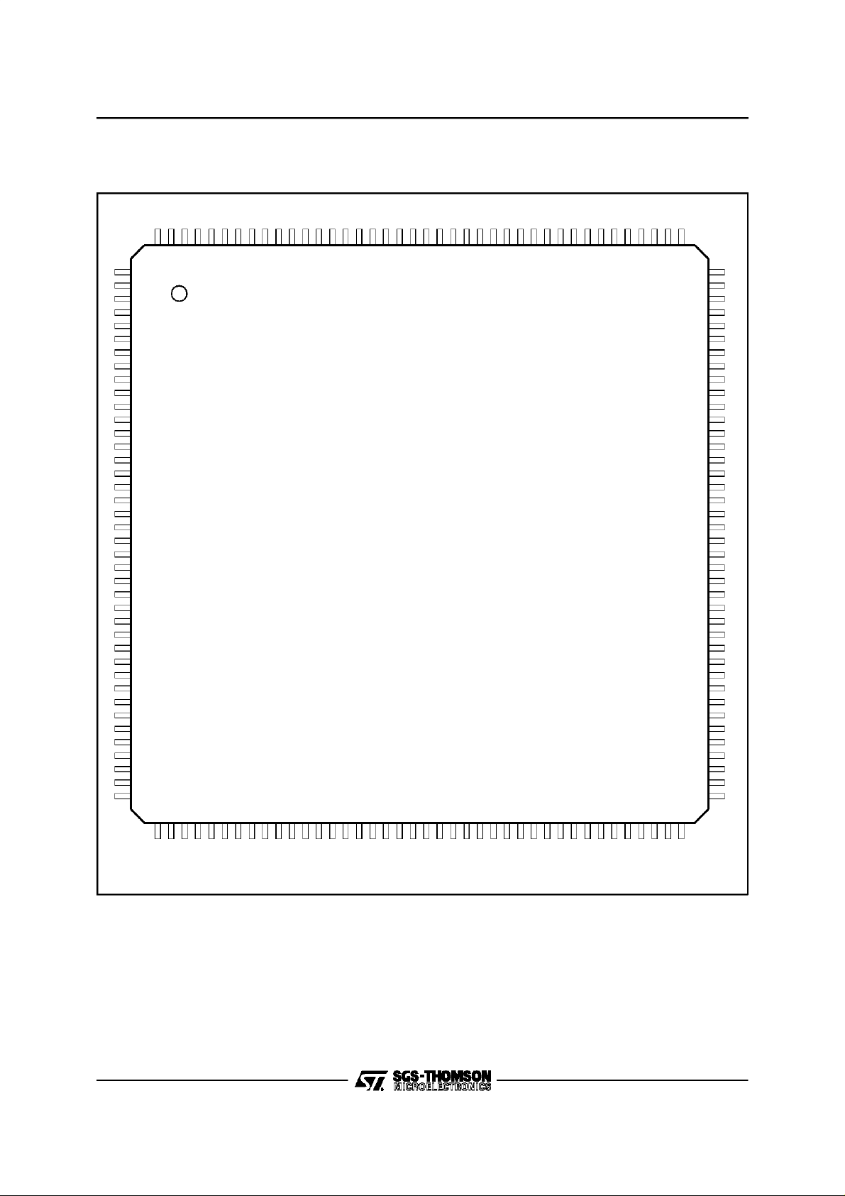
PQFP160PACKAGE
May 1997
s AND SINGLE MICRO-
PQFP160
(Plastic Quad Flat Pack)
ORDER CODE : STLC5464
1/83
Page 2

STLC5464
CONTENTS Page
I PIN INFORMATION .................................................... 8
I.1 PIN CONNECTIONS . . . . . . . . . . .. .. . .. .. . . . ............................. 8
I.2 PIN DESCRIPTION . . . . ................................................ 9
I.3 PIN DEFINITION . . .. . . . . . . . . .. . . . .. . . . . . . . . ........................... 13
I.3.1 Input Pin Definition . .................................................... 13
I.3.2 OutputPin Definition . . . . . . . .. . . . .. . .. .. . . . ............................. 13
I.3.3 Input/OutputPin Definition . .............................................. 13
II BLOCK DIAGRAM .................................................... 14
III FUNCTIONAL DESCRIPTION ........................................... 15
III.1 THE SWITCHINGMATRIX N x 64KBits/S . . .. . . . .. ......................... 15
III.1.1 FunctionDescription . . .. . .. .. . . . . . . . . .. . . . ............................. 15
III.1.2 Architectureof the Matrix . . . . . . . . . . . . .. . . . .. .. .. ......................... 15
III.1.3 ConnectionFunction . . . . . .. .. . . . . . . . . .. . . . ............................. 15
III.1.4 Loop Back Function . . . . ................................................ 15
III.1.5 Delay through the Matrix . . . . . . . . . . . . .. . . . .. . . . . ......................... 17
III.1.5.1 Variable Delay Mode . . . . ............................................. 17
III.1.5.2 Sequence Integrity Mode . . .. .......................................... 17
III.1.6 ConnectionMemory . . .. ................................................ 21
III.1.6.1 Description . . . . . . . .. . . . .. . . . .. . . . . . ................................. 21
III.1.6.2 Accessto ConnectionMemory . . .. . . . .. . .. .............................. 21
III.1.6.3 Accessto DataMemory . .............................................. 21
III.2 HDLC CONTROLLER . ................................................. 21
III.2.1 Functiondescription . . .. ................................................ 21
III.2.1.1 Format of theHDLC Frame . ........................................... 21
III.2.1.2 Compositionof anHDLC Frame . . .. .................................... 21
III.2.1.3 Descriptionand Functions of theHDLC Bytes . .. . . . . . . . . .. . . . .. .. . .. ....... 23
III.2.2 CSMA/CRCapability . . . . . . . . . . .. .. . .. .. . . . ............................. 23
III.2.3 Time Slot Assigner Memory . . .. .......................................... 24
III.2.4 Data Storage Structure . . .. ............................................. 24
III.2.4.1 Reception . . .. ...................................................... 24
III.2.4.2 Transmission . . . . ................................................... 24
III.2.4.3 Frame Relay . ....................................................... 24
III.2.5 TransparentModes . . . . ................................................ 26
III.2.6 Commandof the HDLC Channels . ........................................ 26
III.2.6.1 Reception Control . . .. ................................................ 26
III.2.6.2 TransmissionControl . . .. ............................................. 26
III.3 C/I AND MONITOR . . .. ................................................ 26
III.3.1 FunctionDescription . . .. . .. .. . . . . . . . . .. . . . ............................. 26
III.3.2 GCI and V* Protocol . . .. ................................................ 27
III.3.3 Structureof the Treatment . .............................................. 27
III.3.4 CI and Monitor ChannelConfiguration . ..................................... 27
III.3.5 CI and Monitor Transmission/ReceptionCommand . .. . .. .. . . . . . . . . .. .. . .. .... 27
III.4 MICROPROCESSOR INTERFACE . . .. .................................... 28
III.4.1 Description . .......................................................... 28
III.4.2 Definition of the Interfacefor thedifferent microprocessors . . . .. . . .. ............. 28
2/83
Page 3

STLC5464
CONTENTS
III.5 MEMORYINTERFACE . . . . ............................................. 31
III.5.1 FunctionDescription . . .. . .. .. . . . . . . . . .. . . . ............................. 31
III.5.2 Choiceof memoryversus microprocessorand capacity required . . . . . . ........... 31
III.5.3 MemoryCycle . ....................................................... 31
III.5.4 SRAM interface . . . . ................................................... 32
III.5.4.1 18K x n SRAM . . .. . .. .. . . . . . . . . . . . . . . . . . . ........................... 32
III.5.4.2 512K x n SRAM . .................................................... 32
III.5.5 DRAM Interface . . .. ................................................... 32
III.5.5.1 256K x n DRAM . .................................................... 32
III.5.5.2 1M x n DRAM . . . . ................................................... 33
III.5.5.3 4M x n DRAM . . . . ................................................... 33
III.6 BUS ARBITRATION . . .. ................................................ 33
III.7 CLOCK SELECTIONAND TIME SYNCHRONIZATION . . . .. . .. .. . .. . .. .. . . . . . . 34
III.7.1 ClockDistributionSelection and Supervision. . .. . . . . . . . . . . . . .. .. . .. .......... 34
III.7.2 VCXOFrequency Synchronization. ........................................ 34
III.8 INTERRUPTCONTROLLER . . . . . . . . . . . . .. . . . . . . . . . ...................... 35
III.8.1 Description . .......................................................... 35
III.8.2 OperatingInterrupts(INT0 Pin) . . . . ....................................... 35
III.8.3 Time Base Interrupts (INT1 Pin) . . .. . . . . . . . . .............................. 35
III.8.4 EmergencyInterrupts(WDO Pin) . . ........................................ 35
III.8.5 InterruptQueues . . . . . . . .. . .. .. . .. .. . . .. . . . . ........................... 35
III.9 WATCHDOG . . . . . . . . . . . . .. . . . .. . . . . . ................................. 36
III.10 RESET . . . . . . ...................................................... .. 36
(continued)
Page
IV DC SPECIFICATIONS .................................................. 37
V CLOCK TIMING ....................................................... 38
V.1 SYNCHRONIZATION SIGNALSDELIVEREDBY THE SYSTEM . . . . . . ........... 38
V.2 TDM SYNCHRONIZATION . . . . .......................................... 39
V.3 GCI INTERFACE . . .. . . . .. . . . .. . . . .. . . . . . . . . ........................... 40
V.4 V* INTERFACE . . . . ................................................... 41
VI MEMORYTIMING ..................................................... 42
VI.1 DYNAMICMEMORIES . . .. ............................................. 42
VI.2 STATICMEMORIEs . . .. . .. .. . . . . . . . . .. . . . ............................. 44
VII MICROPROCESSOR TIMING ............................................ 46
VII.1 ST9 FAMILY MOD0=1, MOD1=0, MOD2=0 . . . . . . . . .. . .. . .. .. . . . . . .......... 46
VII.2 80C188MOD0=1, MOD1=1,MOD2=0 . . .. ................................. 48
VII.3 80C186MOD0=1, MOD1=1,MOD2=1 . . .. ................................. 50
VII.4 68000 MOD0=0, MOD1=0,MOD2=1 . . . . . . . .. . . . . . . . . . . . . .. ................ 52
VII.5 TOKEN RING TIMING . ................................................. 54
VII.6 MASTERCLOCK TIMING . .............................................. 54
3/83
Page 4

STLC5464
CONTENTS
VIII INTERNAL REGISTERS ................................................ 55
VIII.1 IDENTIFICATION ANDDYNAMIC COMMAND REGISTER . . . .. . .. . .. IDCR (00)H 55
VIII.2 GENERALCONFIGURATION . ................................. GCR(02)H 55
VIII.3 INPUTMULTIPLEXCONFIGURATION REGISTER0. . . . .. .........IMCR0(04)H 57
VIII.4 INPUTMULTIPLEXCONFIGURATION REGISTER1. . . . .. .........IMCR1(06)H 57
VIII.5 OUTPUTMULTIPLEXCONFIGURATION REGISTER0. .. . . . . . . . . . OMCR0(08)H 57
VIII.6 OUTPUTMULTIPLEXCONFIGURATION REGISTER1. .. . . . . . . . . OMCR1 (0A)H 58
VIII.7 SWITCHING MATRIXCONFIGURATION REGISTER. . . . .. .........SMCR (0C)H 58
VIII.8 CONNECTION MEMORYDATA REGISTER. . .. . . . . .. . .. . .. .. . . . . CMDR(0E)H 59
VIII.9 CONNECTION MEMORYADDRESS REGISTER. .. . .. ............ CMAR (10)H 60
VIII.10 SEQUENCEFAULT COUNTERREGISTER . . . . . . . . .. . .. . .. .. . . . . SFCR(12)H 61
VIII.11 TIME SLOT ASSIGNERADDRESSREGISTER . . . . .. .. . . . . . . . . .. . TAAR (14)H 61
VIII.12 TIME SLOT ASSIGNERDATA REGISTER . . .. .. . .. .............. TADR (16)H 62
VIII.13 HDLC TRANSMIT COMMANDREGISTER . . . . . . . . . .............. HTCR (18)H 62
VIII.14 HDLC RECEIVE COMMAND REGISTER . ....................... HRCR (1A)H 64
VIII.15 ADDRESSFIELD RECOGNITIONADDRESSREGISTER . . . .. . . . . . AFRAR (1C)H 65
VIII.16 ADDRESSFIELD RECOGNITIONDATA REGISTER . . . . .. ........ AFRDR(1E)H 66
VIII.17 FILL CHARACTER REGISTER . . . . ............................. FCR(20)H 66
VIII.18 GCI CHANNELSDEFINITION REGISTER 0 . . .. .. .. . . . . . . . . .. .. . . GCIR0 (22)H 66
VIII.19 GCI CHANNELSDEFINITION REGISTER 1 . . .. .. .. . . . . . . . . .. .. . . GCIR1 (24)H 67
VIII.20 GCI CHANNELSDEFINITION REGISTER 2 . . .. .. .. . . . . . . . . .. .. . . GCIR2 (26)H 67
VIII.21 GCI CHANNELSDEFINITION REGISTER 3 . . .. .. .. . . . . . . . . .. .. . . GCIR3 (28)H 67
VIII.22 TRANSMITCOMMAND / INDICATE REGISTER. . . . .. .. . . . . . . . . .. . . TCIR (2A)H 68
VIII.23 TRANSMITMONITOR ADDRESS REGISTER . . . . . .. .. ........... TMAR(2C)H 69
VIII.24 TRANSMITMONITOR DATA REGISTER . ....................... TMDR(2E)H 70
VIII.25 TRANSMITMONITOR INTERRUPTREGISTER. .. . . . .. .. . .. . .. .. . . TMIR (30)H 70
VIII.26 MEMORYINTERFACECONFIGURATIONREGISTER . .. . .. .. . . . . . . MICR(32)H 70
VIII.27 INITIATEBLOCKADDRESS REGISTER. . . . . . . ................... IBAR (34)H 72
VIII.28 INTERRUPTQUEUESIZE REGISTER. . .. ....................... IQSR(36)H 72
VIII.29 INTERRUPTREGISTER . . .. . .. .. . . . . . . . . .. . . .. ................. IR(38)H 73
VIII.30 INTERRUPTMASK REGISTER. . .. .............................. IMR(3A)H 74
VIII.31 TIME REGISTER . . . . . . . .. . .. .. . .. .. . . .. . . . . ................ TIMR(3C)H 74
VIII.32 TESTREGISTER . . .. . . . .. . .. .. . . . . . . . . . . . .. ................... TR(3E)H 74
(continued)
Page
4/83
Page 5

STLC5464
CONTENTS
IX EXTERNALREGISTERS ............................................... 75
IX.1 NITIALIZATIONBLOCK IN EXTERNALMEMORY . . . . . . . .. ................... 75
IX.2 RECEIVEDESCRIPTOR . . .. . . . .. . .. .. . . . . . . . .. ......................... 76
IX.2.1 Bits writtenby the Microprocessoronly . . . . ................................. 76
IX.2.2 Bits writtenby the Rx DMAConly . ........................................ 76
IX.2.3 Receive Buffer . ....................................................... 76
IX.3 TRANSMITDESCRIPTOR . . .. .......................................... 77
IX.3.1 Bits writtenby the Microprocessoronly . . . . ................................. 77
IX.3.2 Bits writtenby the Rx DMAConly . ........................................ 78
IX.3.3 TransmitBuffer . ....................................................... 78
IX.4 RECEIVE& TRANSMIT HDLC FRAME INTERRUPT . . . . . . .................... 78
IX.5 RECEIVECOMMAND/ INDICATE INTERRUPT . . .. .. ....................... 79
IX.5.1 Receive Command / IndicateInterrupt when TSV = 0 . . . . . . .................... 79
IX.5.2 Receive Command / IndicateInterrupt when TSV = 1 . . . . . . .................... 80
IX.6 RECEIVEMONITORINTERRUPT . . . . .................................... 80
IX.6.1 Receive Monitor Interrupt when TSV = 0 . . . . . . . ............................. 80
IX.6.2 Receive Monitor Interrupt when TSV = 1 . . . . . . . ............................. 81
X PACKAGE MECHANICAL DATA ......................................... 82
(continued)
Page
5/83
Page 6

STLC5464
LISTOF FIGURES Page
I PIN INFORMATION .................................................... 8
II BLOCK DIAGRAM .................................................... 14
Figure1 : General Block Diagram . . .. . . . .. . . . . . . . .. .. . .. ................ 14
III FUNCTIONAL DESCRIPTION ........................................... 15
Figure2 : SwitchingMatrix Data Path . . .. . . . ............................. 16
Figure3 : Unidirectionaland BidirectionalConnections . .. .. . . .. ............. 17
Figure4 : LoopBack . . . . ............................................. 17
Figure5 : Variable Delay through the matrix with ITDM= 1 . .. .. . . .. .......... 18
Figure6 : Variable Delay through the matrix with ITDM= 0 . .. .. . . .. .......... 19
Figure7 : Constant Delay throughthe matrixwith SI = 1 . . . . . . .. .. . .. . .. .. . . . 20
Figure8 : HDLC and DMA ControllerBlock Diagram . .. . . . . . . . . .. .. . .. . .. .. . 22
Figure9 : Structureof theReceive CircularQueue . . . .. . . .. ................ 25
Figure10 : Structureof theTransmitCircular Queue . . . . . . . .. ................ 25
Figure11 : D, C/Iand Monitor Channel Path . . . . . . . .. ...................... 28
Figure12 :
Figure13 :
Figure14 : MicroprocessorInterface for INTEL80C188 . . . . .. ................. 29
Figure15 : MicroprocessorInterface for INTEL80C186 . . . . .. ................. 29
Figure16 : MicroprocessorInterface for MOTOROLA 68000 . . . . . . . .. .......... 30
Figure17 : MicroprocessorInterface for ST9 . . . . . . . .. ...................... 30
Figure18 : 128K x 8 SRAMCircuit Memory Organization . .. .. . .. . .. .. . . . . . . . . 32
Figure19 : 512K x 8 SRAMCircuit Memory Organization . .. .. . .. . .. .. . . . . . . . . 32
Figure20 : 256K x 16 DRAMCircuit Organization . .. . . . .. .. . .. . .. .. . . . . . .... 32
Figure21 : 1M x 16 DRAM Circuit Organization . . . . .. ....................... 33
Figure22 : 4M x 16 DRAM Circuit Organization . . . . .. ....................... 33
Figure23 : Chain of n
Figure24 : MHDLC Clock Generation. . . . ................................. 34
Figure25 : VCXO FrequencySynchronization . . . . . . . . . . . .. .. . .. . .. .. ....... 35
Figure26 : The Three Circular Interrupt Memories . . . . .. .. . . . . . . . . .. .. . .. .... 36
Multi-HDLC
Multi-HDLC
connectedto µP with multiplexed buses . . . .. . . . . ....... 29
connectedto µP with non-multiplexedbuses . . . . .. .. . . . . 29
Multi-HDLC
Components . . . . . . ....................... 33
IV DC SPECIFICATIONS .................................................. 37
V CLOCK TIMING ....................................................... 38
Figure27 : Clocks received and deliveredby the
Figure28 : SynchronizationSignals receivedby the
Figure29 : GCI Synchro Signal delivered by the
Figure30 : V* SynchronizationSignal delivered by the
VI MEMORYTIMING ..................................................... 42
Figure31 : Dynamic Memory Read Signals from the
Figure32 : Dynamic Memory Write Signalsfrom the
Figure33 : Static MemoryRead Signals from the
Figure34 : Static MemoryWrite Signals from the
6/83
Multi-HDLC
Multi-HDLC
Multi-HDLC
Multi-HDLC
Multi-HDLC
Multi-HDLC
Multi-HDLC
Multi-HDLC
.................. 38
................ 39
................... 40
.............. 41
............... 42
............... 43
.................. 44
.................. 45
Page 7

STLC5464
LISTOF FIGURES
VII MICROPROCESSOR TIMING ............................................ 46
Figure35 : ST9 Read Cycle . ........................................... 46
Figure36 : ST9 Write Cycle . ........................................... 47
Figure37 : 80C188 Read Cycle . ........................................ 48
Figure38 : 80C188 WriteCycle . ........................................ 49
Figure39 : 80C186 Read Cycle . ........................................ 50
Figure40 : 80C186 WriteCycle . ........................................ 51
Figure41 : 68000 Read Cycle . .. .. . . . . .................................. 52
Figure42 : 68000 Write Cycle . . . . ....................................... 53
Figure43 : Token Ring . . . . . . . . . . .. .. . . . . . . . .. ......................... 54
Figure44 : MasterClock . .............................................. 54
VIII INTERNAL REGISTERS ................................................ 55
IX EXTERNALREGISTERS ............................................... 75
X PACKAGE MECHANICAL DATA ........................................ 82
(continued)
Page
7/83
Page 8
STLC5464
I - PIN INFORMATION
I.1 - Pin Connections
SSVDD
NTEST
V
160
159
NRESET
1
XTAL1
2
XTAL2
3
WDO
4
CB
5
EC
6
VCXO IN
7
VCXO OUT
8
9
DCLK
10
CLOCKA
11
CLOCKB
12
FRAMEA
13
FRAMEB
14
V
DD
15
V
SS
16
FS
17
FSCG
18
FSCV
19
PSS
20
DIN0
21
DIN1
22
DIN2
23
DIN3
24
DIN4
25
DIN5
26
DIN6
27
DIN7
28
DIN8
29
V
DD
30
V
SS
31
DOUT0
32
DOUT1
33
DOUT2
34
DOUT3
35
DOUT4
36
DOUT5
37
DOUT6
38
DOUT7
39
NDIS
40
NTRST
158
DM15
157
DM14
156
DM13
155
DM12
154
DM11
153
DM10
152
DM9
151
DM8
150
414243444546474849505152535455565758596061626364656667686970717273747576777879
DM7
149
DM6
148
DM5
147
SSVDD
V
146
145
DM4
144
DM3
143
DM2
142
DM1
141
DM0
140
ADM14
ADM13
139
138
ADM12
ADM11
137
136
VSSV
ADM10
135
134
133
DD
ADM9
ADM8
ADM7
ADM6
ADM5
ADM4
ADM3
ADM2
132
131
130
129
128
127
126
125
ADM1
ADM0
124
123
NRAS3/NCE6
NRAS2/NCE4
NCAS1/NCE3
NRAS1/NCE2
NCAS0/NCE1
NRAS0/NCE0
A23/ADM18
A22/ADM17
A21/ADM16
A20/ADM15
VSSV
122
DD
121
NCE7
NCE5
NOE
NWE
TRO
TRI
D15
D14
D13
D12
D11
D10
A19
A18
A17
A16
120
119
118
117
116
115
114
113
112
111
110
109
108
V
SS
107
V
DD
106
105
104
103
102
101
100
D9
99
D8
98
D7
97
D6
96
D5
95
D4
94
D3
93
D2
92
D1
91
D0
90
V
SS
89
V
DD
88
87
86
85
84
83
82
81
80
8/83
TMS
TDI
TDO
TCK
SS
DD
V
V
NCS0
NCS1
INT0
INT1
NLDS
NBHE/NUDS
READY
NDTACK
NAS/ALE
R/W / NWR
MOD0
NDS/NRD
MOD1
MOD2
SS
DD
V
V
A0/AD0
A1/AD1
A2/AD2
A3/AD3
A4/AD4
A5/AD5
A6/AD6
A7/AD7
A8/AD8
A9/AD9
SS
DD
V
V
A10/AD10
A11/AD11
A12/AD12
A13/AD13
A14/AD14
A15/AD15
5464-01.EPS
Page 9
STLC5464
I - PIN INFORMATION(continued)
I.2 - Pin Description
Pin N° Symbol Type Function
POWER PINS (all thepower and ground pins must be connected)
14 V
15 V
29 V
30 V
45 V
46 V
61 V
62 V
73 V
74 V
89 V
90 V
107 V
108 V
121 V
122 V
133 V
134 V
145 V
146 V
158 V
159 V
DD1
SS1
DD2
SS2
DD3
SS3
DD4
SS4
DD5
SS5
DD6
SS6
DD7
SS7
DD8
SS8
DD9
SS9
DD10
SS10
DD11
SS11
CLOCKS
2 XTAL1 I Crystal 1. A clockpulse at f
3 XTAL2 O Crystal 2. If the internal crystal oscillator is used, the second crystal pin isapplied
7 VCXO IN O4 VCXO input signal. This signal is compared to clock A(or B) selected inside the
8 VCXO OUT I3 VCXO error signal. This pin delivers the result of the comparison.
10 CLOCKA I3 Input Clock A (4096kHz or 8192kHz)
11 CLOCKB I3 Input Clock B (4096kHz or 8192kHz)
12 FRAMEA I3 Clock A at 8kHz
13 FRAMEB O8 Clock B at 8kHz
9 DCLK O8 Data Clock issuedfrom Input Clock A (or B). This clock is delivered by the circuit
17 FSCG O8 Frame synchronization for GCI at 8kHz. This clockis issued from FRAME A (or B).
18 FSCV* I3 Frame synchronization for V Star at 8kHz
16 FS O8 Frame synchronization.This signal synchronizesDIN0/7 and DOUT0/7.
19 PSS I3 Programmable synchronization Signal. The PS bit of connection memory is read
Type : I1 = Input TTL ; I2 = I1 + Pull-up ; I3 = I1 + Hysteresis ; I4 = I3 + Pull-up ;
O4 = Output CMOS 4mA ; O4T = O4 + Tristate ; O8 = Output CMOS 8mA, ”1” and ”0” at Low Impedance ;
O8D = OutputCMOS 8mA,Open Drain ; O8DT = Output CMOS 8mA, Open Drainor Tristate;
O8T = OutputCMOS 8mA, Tristate
Power DC supply
Ground DC ground
Power DC supply
Ground DC ground
Power DC supply
Ground DC ground
Power DC supply
Ground DC ground
Power DC supply
Ground DC ground
Power DC supply
Ground DC ground
Power DC supply
Ground DC ground
Power DC supply
Ground DC ground
Power DC supply
Ground DC ground
Power DC supply
Ground DC ground
Power DC supply
Ground DC ground (Total22)
of two crystal pins) with : -50.10
to this output.
Multi-HDLC
.
at 4096kHz(or2048kHz). DOUT0/7 aretransmittedon the risingedge of thissignal.
DIN0/7 are sampled on the fallingedge of this signal.
in real time.
= 32000kHz can be applied to this input (or one pin
Min.
-6
< ∆f < +50.10-6.
9/83
Page 10
STLC5464
I - PIN INFORMATION(continued)
I.2 - Pin Description (continued)
Pin N° Symbol Type Function
TIMEDIVISION MULTIPLEXES (TDM)
20 DIN0 I1 TDM0Data Input 0
21 DIN1 I1 TDM1Data Input 1
22 DIN2 I1 TDM2Data Input 2
23 DIN3 I1 TDM3Data Input 3
24 DIN4 I1 TDM4Data Input 4
25 DIN5 I1 TDM5Data Input 5
26 DIN6 I1 TDM6Data Input 6
27 DIN7 I1 TDM7Data Input 7
28 DIN8 I1 TDM8Data Input 8
31 DOUT0 O8DT TDM0 Data Output0
32 DOUT1 O8DT TDM1 Data Output1
33 DOUT2 O8DT TDM2 Data Output2
34 DOUT3 O8DT TDM3 Data Output3
35 DOUT4 O8DT TDM4 Data Output4
36 DOUT5 O8DT TDM5 Data Output5
37 DOUT6 O8DT TDM6 Data Output6
38 DOUT7 O8DT TDM7 Data Output7
39 NDIS I1 DOUT 0/7 Not Disable. When this pin is at 0V, the Data Output 0/7 are at high
5 CB O8D Contention Bus for CSMA/CR
6 EC I1 Echo. Wired at VSS if not used.
BOUDARY SCAN
40 NTRST I4 Reset for boundary scan
41 TMS I2 Mode Selection for boundary scan
42 TDI I2 Input Data for boundary scan
43 TDO O4 Output Datafor boundary scan
44 TCK I4 Clock for boundary scan
MICROPROCESSOR INTERFACE
58 MOD0 I1 1 1 0 1
59 MOD1 I1 1 1 0 0
60 MOD2 I1 0 1 1 0
1 NRESET I3 CircuitReset
47 NCS0 I3 Chip Select 0 : internal registers are selected
48 NCS1 I3 Chip Select 1 : external memory isselected
49 INT0 O4 Interrupt generated by HDLC, RxC/Ior RxMON. Active high.
50 INT1 O4 Interrupt1.This pin goes to 5V when the selected clock A (or B) has disappeared ;
4 WDO O4 Watch Dog Output.This pingoes to5V during1ms when the microprocessor has not
Type : I1 = Input TTL ; I2 = I1 + Pull-up ; I3 = I1 + Hysteresis ; I4 = I3 + Pull-up ;
O4 = Output CMOS 4mA ; O4T = O4 + Tristate ; O8 = Output CMOS 8mA, ”1” and ”0” at Low Impedance ;
O8D = OutputCMOS 8mA,Open Drain ; O8DT = Output CMOS 8mA, Open Drainor Tristate;
O8T = OutputCMOS 8mA, Tristate
impedance. Wired at VDD if not used.
80C188 80C186 68000 ST9
250µs after resetthis pin goesto 5V also if clock A is not present.
reset the Watch Dog during the programmable time.
10/83
Page 11

I - PIN INFORMATION(continued)
I.2 - Pin Description (continued)
Pin N° Symbol Type Function
MICROPROCESSOR INTERFACE (continued)
51 NLDS I3 Lower Data Strobe (68000)
52 NUDS I3 Bus High Enable (Intel) / Upper Data Strobe(68000)
53 NDTACK O8D Data Transfer Acknowledge (68000)
54 READY O8T Data TransferAcknowledge (Intel)
55 NAS/ALE I3 Address Strobe(Motorola) / Addresss Latch Enable(Intel)
56 R/W / NWR I3 Read/Write (Motorola) /Write(Intel)
57 NDS/NRD I3 Data Strobe (Motorola)/Read Data(Intel)
63 A0/AD0 I/O Address bit 0 (Motorola) / Address/Data bit 0 (Intel)
64 A1/AD1 I/O Address bit 1 (Motorola) / Address/Data bit 1 (Intel)
65 A2/AD2 I/O Address bit 2 (Motorola) / Address/Data bit 2 (Intel)
66 A3/AD3 I/O Address bit 3 (Motorola) / Address/Data bit 3 (Intel)
67 A4/AD4 I/O Address bit 4 (Motorola) / Address/Data bit 4 (Intel)
68 A5/AD5 I/O Address bit 5 (Motorola) / Address/Data bit 5 (Intel)
69 A6/AD6 I/O Address bit 6 (Motorola) / Address/Data bit 6 (Intel)
70 A7/AD7 I/O Address bit 7 (Motorola) / Address/Data bit 7 (Intel)
71 A8/AD8 I/O Address bit 8 (Motorola) / Address/Data bit 8 (Intel)
72 A9/AD9 I/O Address bit 9 (Motorola) / Address/Data bit 9 (Intel)
75 A10/AD10 I/O Address bit 10 (Motorola) / Address/Data bit 10 (Intel)
76 A11/AD11 I/O Address bit 11 (Motorola) / Address/Data bit 11 (Intel)
77 A12/AD12 I/O Address bit 12 (Motorola) / Address/Data bit 12 (Intel)
78 A13/AD13 I/O Address bit 13 (Motorola) / Address/Data bit 13 (Intel)
79 A14/AD14 I/O Address bit14 (Motorola) / Address/Data bit 14 (Intel)
80 A15/AD15 I/O Address bit15 (Motorola) / Address/Data bit 15 (Intel)
81 A16 I1 Address bit16 (Motorola) / Address bit 16 (Intel)
82 A17 I1 Address bit17 (Motorola) / Address bit 17 (Intel)
83 A18 I1 Address bit18 (Motorola) / Address bit 18 (Intel)
84 A19 I1 Address bit19 (Motorola) / Address bit 19 (Intel)
85 A20/ADM15 I/O Address bit 20 from µP (input) / Address bit 15 forSRAM (output)
86 A21/ADM16 I/O Address bit 21 from µP (input) / Address bit 16 forSRAM (output)
87 A22/ADM17 I/O Address bit 22 fromµP (input) / Addressbit 17 for SRAM (output)
88 A23/ADM18 I/O Address bit 23 from µP (input) / Address bit 18 forSRAM (output)
91 DO I/O Data bit 0 for µP ifnot multiplexed (seeNote 1).
92 D1 I/O Data bit 1forµP if not multiplexed
93 D2 I/O Data bit 2for µP if not multiplexed
94 D3 I/O Data bit 3for µP if not multiplexed
95 D4 I/O Data bit 4forµP if not multiplexed
96 D5 I/O Data bit 5for µP if not multiplexed
97 D6 I/O Data bit 6for µP if not multiplexed
98 D7 I/O Data bit 7forµP if not multiplexed
99 D8 I/O Data bit 8for µP if not multiplexed
Type : I1 = Input TTL ; I2 = I1 + Pull-up ; I3 = I1 + Hysteresis ; I4 = I3 + Pull-up ;
O4 = Output CMOS 4mA ; O4T = O4 + Tristate ; O8 = Output CMOS 8mA, ”1” and ”0” at Low Impedance ;
O8D = OutputCMOS 8mA,Open Drain ; O8DT = Output CMOS 8mA, Open Drainor Tristate;
O8T = OutputCMOS 8mA, Tristate
STLC5464
11/83
Page 12
STLC5464
I - PIN INFORMATION(continued)
I.2 - Pin Description (continued)
Pin N° Symbol Type Function
MICROPROCESSOR INTERFACE (continued)
100 D9 I/O Data bit 9for µP if not multiplexed
101 D10 I/O Data bit 10for µP if not multiplexed
102 D11 I/O Data bit 11forµP if not multiplexed
103 D12 I/O Data bit 12for µP if not multiplexed
104 D13 I/O Data bit 13for µP if not multiplexed
105 D14 I/O Data bit 14forµP if not multiplexed
106 D15 I/O Data bit 15for µP if not multiplexed
MEMORY INTERFACE
109 TRI I3 Token Ring Input (foruse
110 TRO O4 Token Ring Output (for use
111 NWE O4T Write Enable for memory circuits
112 NOE O4T Control Output Enable for memory circuits
113 NRAS0/NCE0 O4T Row Address Strobe Bank0 / Chip Enable0 for SRAM
114 NCAS0/NCE1 O4T Column Address StrobeBank 0 / Chip Enable1 for SRAM
115 NRAS1/NCE2 O4T Row Address Strobe Bank1 / Chip Enable2 for SRAM
116 NCAS1/NCE3 O4T Column Address StrobeBank 1 / Chip Enable 3 for SRAM
117 NRAS2/NCE4 O4T Row Address Strobe Bank2 / Chip Enable4 for SRAM
118 NCE5 O4T Chip Enable 5 for SRAM
119 NRAS3/NCE6 O4T Row Address Strobe Bank3 / Chip Enable6 for SRAM
120 NCE7 O4T Chip Enable 7 for SRAM
123 ADM0 O8T Address bit 0for SRAM and DRAM
124 ADM1 O8T Address bit 1for SRAM and DRAM
125 ADM2 O8T Address bit 2for SRAM and DRAM
126 ADM3 O8T Address bit 3for SRAM and DRAM
127 ADM4 O8T Address bit 4for SRAM and DRAM
128 ADM5 O8T Address bit 5for SRAM and DRAM
129 ADM6 O8T Address bit 6for SRAM and DRAM
130 ADM7 O8T Address bit 7for SRAM and DRAM
131 ADM8 O8T Address bit 8for SRAM and DRAM
132 ADM9 O8T Address bit 9for SRAM and DRAM
135 ADM10 O8T Address bit 10 for SRAM and DRAM
136 ADM11 O8T Address bit 11 for SRAM only
137 ADM12 O8T Address bit 12 for SRAM only
138 ADM13 O8T Address bit 13 for SRAM only
139 ADM14 O8T Address bit 14 for SRAM only
Type : I1 = Input TTL ; I2 = I1 + Pull-up ; I3 = I1 + Hysteresis ; I4 = I3 + Pull-up ;
O4 = Output CMOS 4mA ; O4T = O4 + Tristate ; O8 = Output CMOS 8mA, ”1” and ”0” at Low Impedance ;
O8D = OutputCMOS 8mA,Open Drain ; O8DT = Output CMOS 8mA, Open Drainor Tristate;
O8T = OutputCMOS 8mA, Tristate
Multi-HDLC
Multi-HDLC
s in cascade)
s in cascade)
12/83
Page 13
STLC5464
I - PIN INFORMATION(continued)
I.2 - Pin Description (continued)
Pin N° Symbol Type Function
MEMORY INTERFACE (continued)
140 DM0 I/O Memory Data bit 0
141 DM1 I/O Memory Data bit 1
142 DM2 I/O Memory Data bit 2
143 DM3 I/O Memory Data bit 3
144 DM4 I/O Memory Data bit 4
147 DM5 I/O Memory Data bit 5
148 DM6 I/O Memory Data bit 6
149 DM7 I/O Memory Data bit 7
150 DM8 I/O Memory Data bit 8
151 DM9 I/O Memory Data bit 9
152 DM10 I/O Memory Data bit 10
153 DM11 I/O Memory Data bit 11
154 DM12 I/O Memory Data bit 12
155 DM13 I/O Memory Data bit 13
156 DM14 I/O Memory Data bit 14
157 DM15 I/O Memory Data bit 15
160 NTEST I2 Test Control. When this pin is at 0V each output is high impedance except XTAL2 Pin.
Type : I1 = Input TTL ; I2 = I1 + Pull-up ; I3 = I1 + Hysteresis ; I4 = I3 + Pull-up ;
O4 = Output CMOS 4mA ; O4T = O4 + Tristate ; O8 = Output CMOS 8mA, ”1” and ”0” at Low Impedance ;
O8D = OutputCMOS 8mA,Open Drain ; O8DT = Output CMOS 8mA, Open Drainor Tristate;
O8T = OutputCMOS 8mA, Tristate
Note : D0/15 input/output pins must be connectedto one single externalpull up resistor if not used.
I.3 - Pin Definition
I.3.1- Input Pin Definition
I1 : Input1 TTL
I2 : Input2 TTL+ pull-up
I3 : Input3 TTL+ hysteresis
I4 : Input4 TTL+ hysteresis +pull-up
I.3.2- Output Pin Definition
O4 : OutputCMOS 4mA
O4T : OutputCMOS4mA, Tristate
O8 : OutputCMOS 8mA
O8T : OutputCMOS8mA,Tristate
O8D : Output CMOS 8mA,OpenDrain
O8DT : OutputCMOS 8mA,Open Drain or Tristate(Programmablepin)
Moreover, each output is high impedance when theNTEST Pin isat 0 volt except XTAL2 Pin.
I.3.3- Input/Output Pin Definition
I/O: InputTTL/ Output CMOS 8mA.
N.B. XTAL1 : this inputis CMOS.
XTAL2 : NTESTpin at 0 hasno effecton thispin.
13/83
Page 14
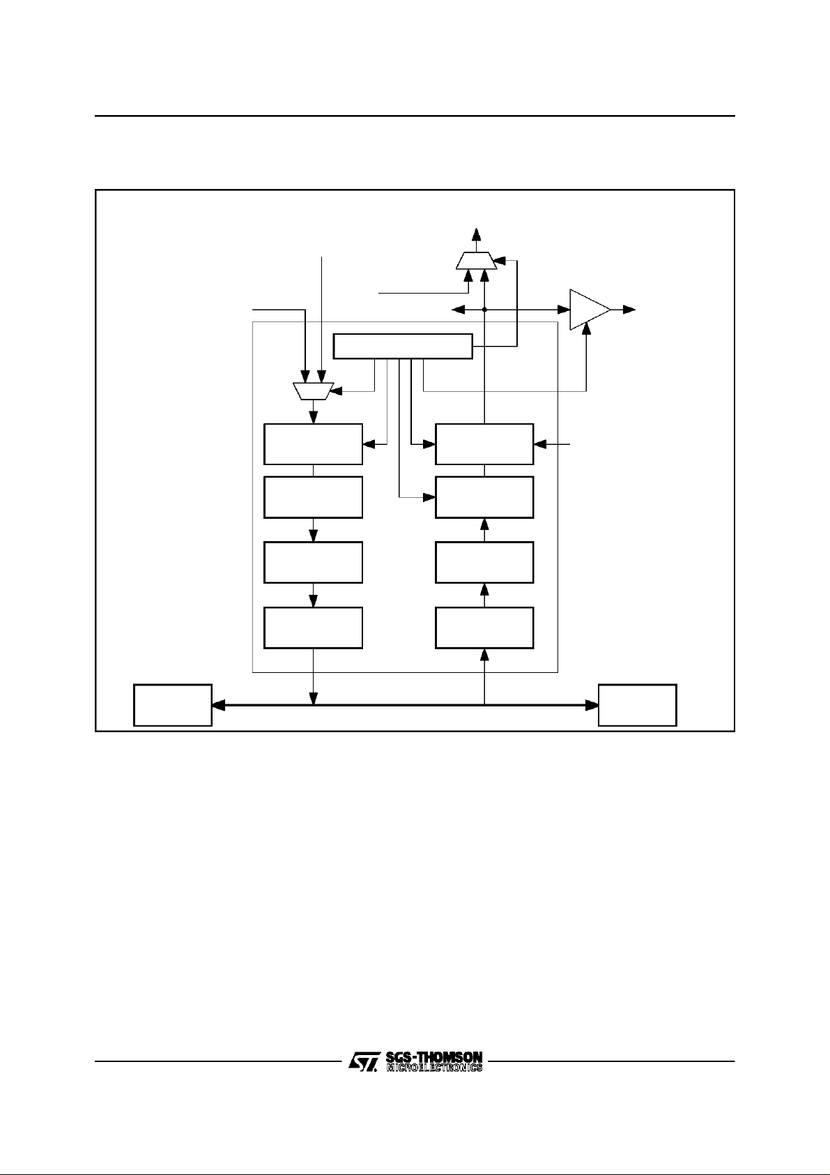
STLC5464
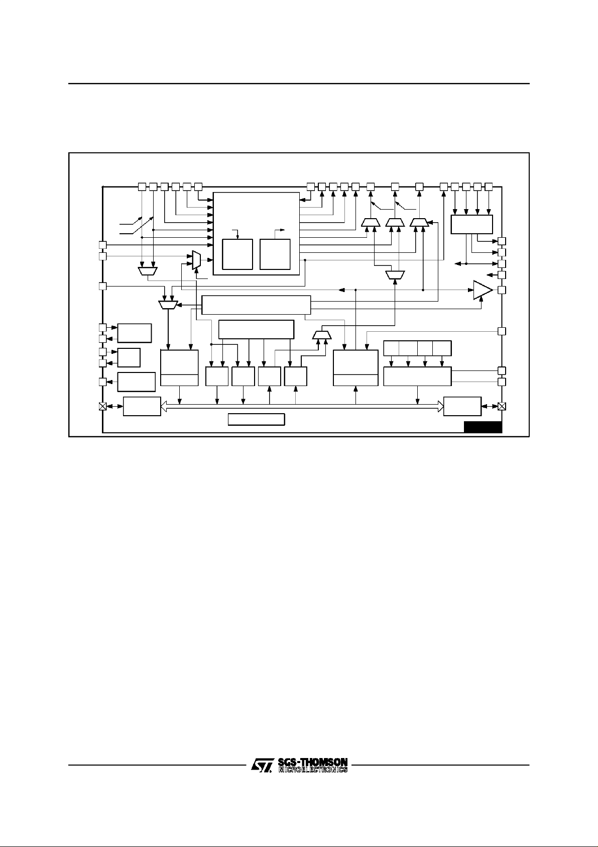
II - BLOCKDIAGRAM
Thetop levelfunctionalities of
Figure1 : GeneralBlock Diagram
DIN5
DIN4
DIN3
25 24 23 22 21 20
GCI1
GCI0
DIN6
26
DIN7
27
DIN8
28
VCX IN
7
8
2
3
4
COUNTER
XTAL
WATCHDOG
32 Rx HDLC
with Adress
Recognition
32 Rx DMAC
VCX OUT
XTAL1
XTAL2
WDO
Multi-HDLC
DIN2
DIN1
DIN0
D7
V10
TIME SLOT ASSIGNER FOR MULTIHDLC
16 Rx
appearon the general block diagram.
0
SWITCHING MATRIX
1
n x64 kb/s
2
3
4
5
6
Pseudo
Random
Sequence
7
Analyser
GCI CHANNELDEFINITION
C/I
16 Rx
MON
Sequence
Generator
16 Tx
Pseudo
Random
C/I
NDIS
39 31 32 33 34
0
1
2
3
4
5
6
7
16 Tx
MON
DOUT0
DOUT1
32 Tx HDLC
with CSMA CR
for Content.Bus
32 Tx DMAC
DOUT2
DOUT3
DOUT4
35
DOUT537DOUT6
36
GCI0
GCI1
Rx
C/IRxMONTxC/ITxMON
INTERRUPT
CONTROLLER
DOUT712FRAME A10CLOCK A13FRAME B11CLOCK B
38
V10
To
Internal
Circuit
CLOCK
SELECTION
18
FSCV*
17
FSCG
9
DCLK
16 FS
5CB
6EC
49 INT0
50 INT1
µP Bus
µP
INTERFACE
Internal Bus
BUS ARBITRATION
Thereare :
- The switching matrix,
- The time slot assigner,
- The 32 HDLC transmitters with associated DMA
controllers,
- The 32 HDLC receivers with associated DMA
controllers,
- The 16 Command/Indicateand MonitorChannel
transmitters belonging to two General Component Interfaces(GCI),
RAM
INTERFACE
RAM
Bus
STLC5464
- The 16 Command/Indicateand Monitor Channel
receivers belonging to two General Component
Interfaces(GCI),
- The memoryinterface,
- The microprocessor interface,
- The bus arbitration,
- The clock selection and time synchronization
function,
- The interruptcontroller,
- The watchdog,
5464-02.EPS
14/83
Page 15

III - FUNCTIONAL DESCRIPTION
III.1- The SwitchingMatrix N x 64 KBits/S
III.1.1 - Function Description
The matrix performs a non-blockingswitch of 256
time slots from 8 Input Time Division Multiplex
(TDM) at 2 Mbit/sto 8 output Time Division Multiplex.A TDM is composedof 32 TimeSlots (TS)at
64 kbit/s. The matrix is designed to switch a 64
kbit/s channel (Variable delay mode) or an hyperchannel of data (Sequence integrity mode).So, it
will both provide minimum throughput switching
delayfor voiceapplicationsandtimeslotsequence
integrity for data applications on a per channel
basis.
The requirements of theSequence Integrity(n*64
kbit/s)mode are the following:
Allthe time slotsof agiveninputframemust beput
out during a same output frame.
The time slots of an hyperchannel(concatenation
of TS in the same TDM) are not crossed together
at output in different frames.
In variable delay mode, the time slot is put out as
soon as possible. (The delay is two or three time
slots minimum between input and output).
For test facilities, any time slot of an OutputTDM
(OTDM) can be internally looped back into the
sameInput TDM number(ITDM) at thesame time
slotnumber.
A Pseudo Random Sequence Generator and a
Pseudo Random Sequence Analyzer are implemented in thematrix. They allowthe generationa
sequence on a channel or on a hyperchannel,to
analyse it and verify its integrity after several
switching in the matrix or some passing of the
sequenceacross different boards.
The Frame Signal (FS) synchronises ITDM and
OTDMbut a programmabledelay or advancecan
beintroducedseparatelyoneachITDMand OTDM
(a half bit time, a bittime or two bit times).
An additionalpin (PSS) permitsthe generationof
a programmable signal composed of 256 bits per
frameat abit rate of 2048 kbit/s.
STLC5464
An externalpin (NDIS) asserts a high impedance
on all the TDM outputs of the matrix when active
(duringthe initialization of theboard for example).
III.1.2 - Architecture of the Matrix
The matrix is essentially composed of buffer data
memoriesand a connection memory.
Thereceivedserialdatais firstconvertedtoparallel
byaserialto parallelconverterandstoredconsecutively in a 256 position Buffer Data Memory (see
Figure 2 onPage 16).
To satisfy the Sequence Integrity (n*64 kbit/s) requirements,the data memoryis built with an even
memory, an odd memory and an output memory.
Twoconsecutiveframesare storedalternatively in
theoddandevenmemory.Duringthe timeaninput
frame is stored, the one previouslystoredis transferred into the output memory according to the
connectionmemoryswitchingorders.Aframelater,
the outputmemoryis readand datais convertedto
serial and transferred to the outputTDM.
III.1.3 - ConnectionFunction
Twotypes of connectionsare offered:
- unidirectionalconnection and
- bidirectionalconnection.
Anunidirectionalconnectionmakesonlytheswitch
ofaninputtimeslotthroughan outputonewhereas
abidirectionalconnectionestablishesthelinkin the
other direction too. So a doubleconnectioncan be
achieved by a single command (see Figure 3 on
Page 17).
III.1.4 - LoopBack Function
Any time slot of an Output TDM can be internally
looped back on the timeslot which has the same
TDM numberand the same TS number
(OTDMi,TSj) ----> (ITDMi, TSj).
In the case of a bidirectional connection, only the
one specified by the microprocessoris concerned
by the loop back (see Figure 4 onPage 17).
15/83
Page 16
STLC5464
III - FUNCTIONAL DESCRIPTION(continued)
Figure2 :SwitchingMatrixData Path
D7 DIN’ 0/7 D4/5
Tx
HDLC
HDLCM 1
LOOP
IMTD
Sequence
Integrity
DIN 0/7
BIT SYNCHRO
1
S/P
DATA
MEMORIES
64kb/sand
n x 64kb/s
PRSG : Pseudo RandomSequence Generator
PRSA : PseudoRandom Sequence Analyzer
OTSV : OutputTime Slot Validated
From Connection
Memory
INS : Insert
CM : ConnectionMemory (from CMAR Register)
ME : Message Enable
Rx
GCI
PRSG
PSEUDORANDOM
SEQUENCE
GENERATOR
Rec. O.152
1
A
IMTD : Increased Min Throughtput Delay
SGV : SequenceGenerator Validated
SAV: SequenceAnalyzer Validated
SGV
1
CM
211-1
(whenRead)
CONNECTION
MEMORY
DD
From SMCR Register
Internal
Bus
CMDR
Sequence Integrity,
Data
Register
CMAR
CM
LOOP, PRSA,PRSG,
INS, OTSV
1
D0/7
16/83
Tx
GCI
INS
GCIR
ME
D4/5
1
BIT SYNCHRO
DOUT 0/7
1
P/S
Address
PRSG
1
Rx
HDLC
D7
PRSA
PSEUDORANDOM
SEQUENCE
ANALYZER
Rec. O.152
SAV
211-1
Register
SFDR
SequenceFault
CounterRegister
From Connection Memory
OTSV (per channel)
From OMCR Register
OMV (per multiplex)
From Disable Pin
(for all multiplexes)
5464-03.EPS
Page 17
III - FUNCTIONAL DESCRIPTION(continued)
Figure3 :Unidirectionaland Bidirectional Connections
STLC5464
Figure4 : LoopBack
OTSy, OTDMq
DOWN STREAM
OTSy, OTDMq
DOWN STREAM
OTSy, OTDMq
DOWN STREAM
ITSy, ITDMq
UP STREAM
DATA
MEMORY
n x 64kb/s
Unidirectional Connection
DATA
MEMORY
n x 64kb/s
DATA
MEMORY
n x 64kb/s
Bidirectional Connection
OTSV
DATA
MEMORY
n x 64kb/s
ITSx,ITDMp
DOWN STREAM
ITSx,ITDMp
DOWN STREAM
OTSx, OTDMp
UP STREAM
DOWN STREAM
p, q = 0 to7
x, y = 0 to 31
ITSx,ITDMp
5464-04.EPS
ITSy, ITDMq
UP STREAM
Loopback per channel relevant if bidirectional connection has been done.
III.1.5 - Delay through the Matrix
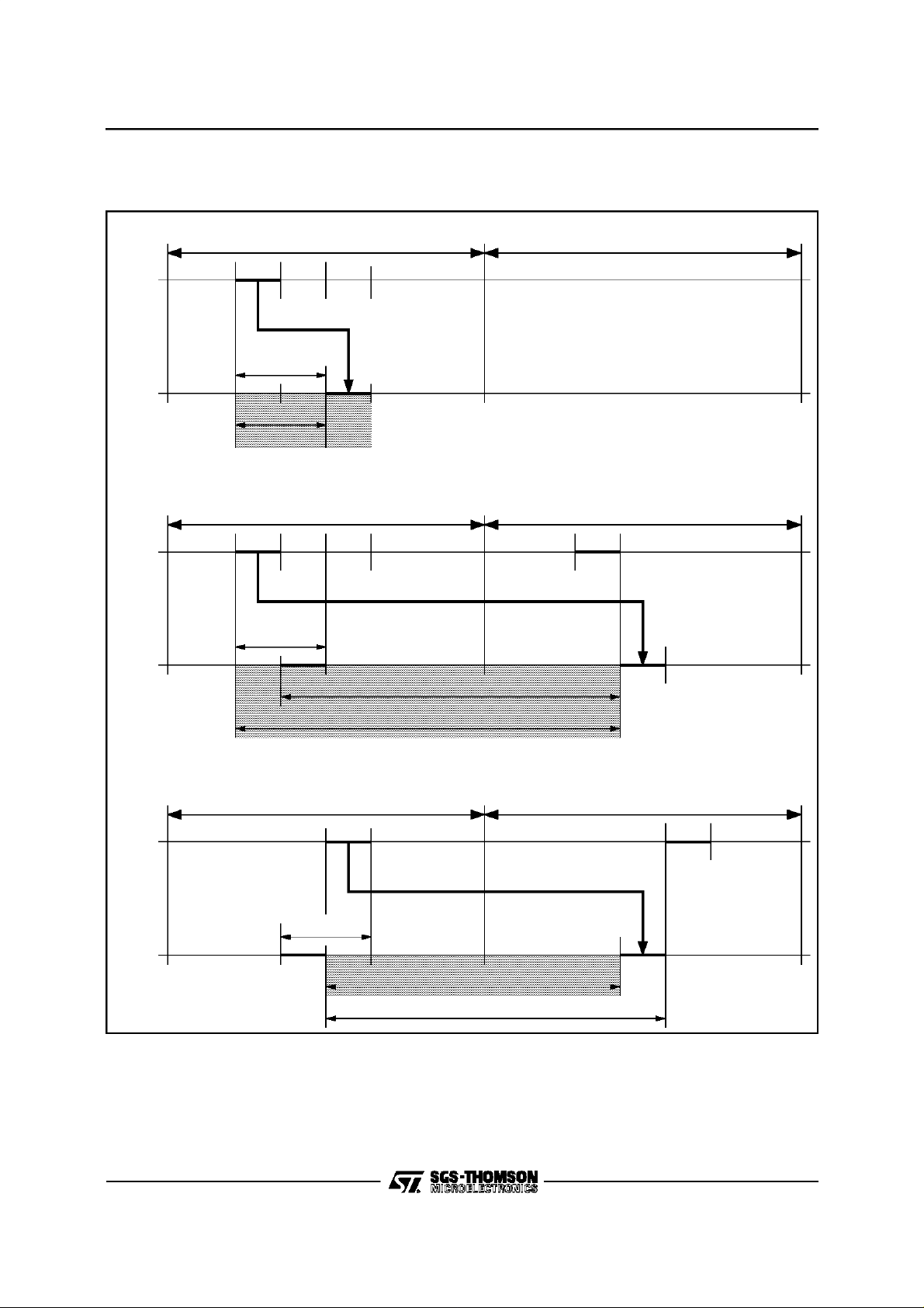
III.1.5.1- VariableDelay Mode
In the variable delay mode, the delay through the
matrixdependsontherelativepositionsof theinput
and output time slots in the frame.
So,some limits are fixed:
- the maximumdelay is a frame+ 2time slots,
- the minimum delay is programmable.
Three time slotsifIMTD = 1, inthis case n = 2 in
the fo rmula he reafter or two time slots if
IMTD = 0, in this case n = 1 inthe sameformula
(see Paragraph ”Switching Matrix Configuration
Reg SMCR (0C)H” on Page60).
Allthe possibilitiescan be rankedin three cases :
a) If OTSy> ITSx+ n then the variable delay is :
OTSy- ITSxTime slots
DATA
MEMORY
n x 64kb/s
Loop
OTSx, OTDMp
UP STREAM
p, q = 0 to 7
x, y = 0 to 31
b) IfITSx<OTSy< ITSx+ n thenthevariabledelay
is :
OTSy - ITSx+ 32 Timeslots
c) OTSy < ITSxthenthe variable delay is :
32 - (ITSx- OTSy)Time slots.
N.B. Ruleb) andrule c) are identical.
For n = 1 and n =2, see Figure 5 on Page 18.
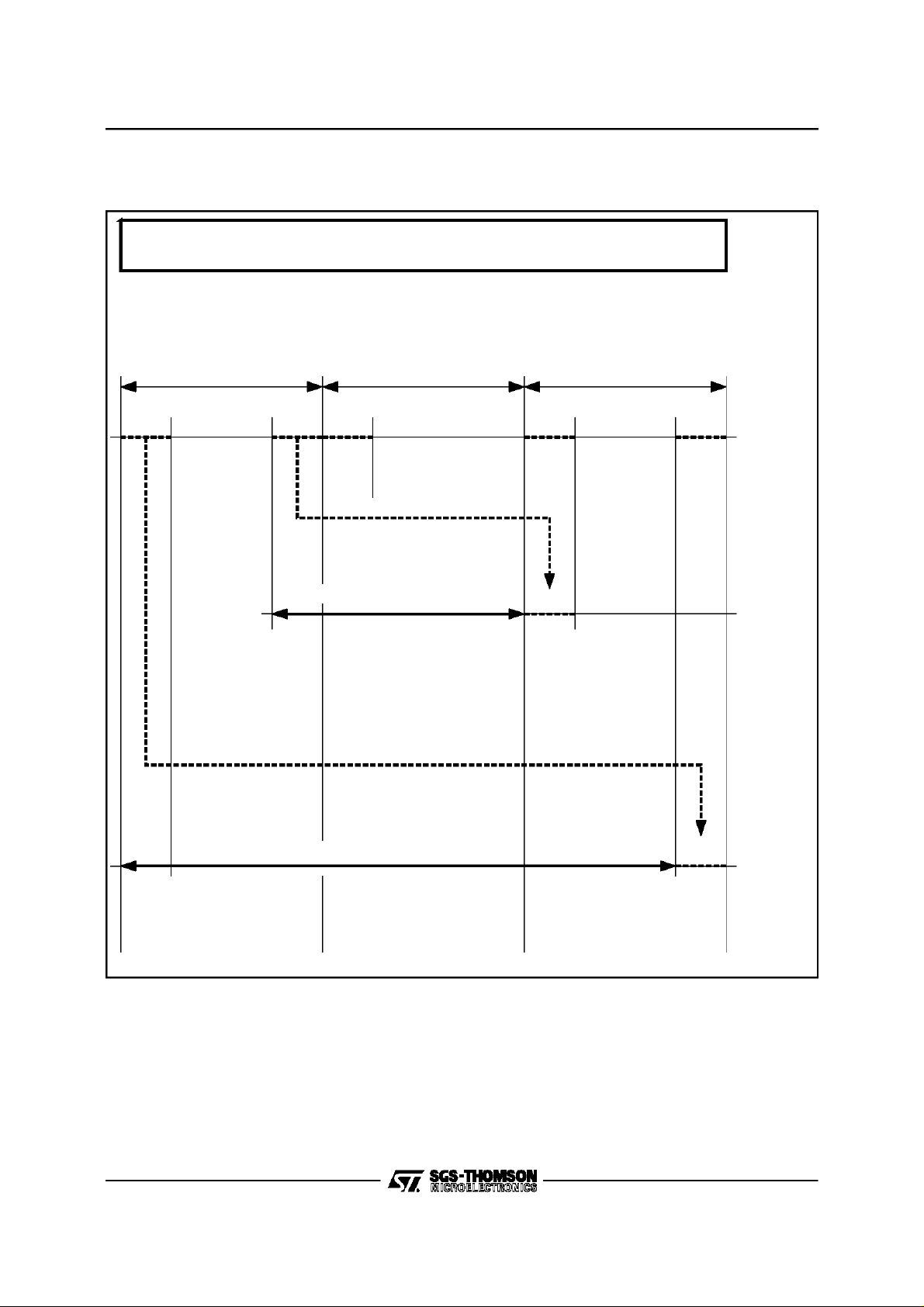
III.1.5.2- SequenceIntegrity Mode
In the sequenceintegrity mode (SI = 1, bit located
in theConnectionMemory),theinputtimeslotsare
put out 2 frames later (see Figure 6 on Page 19).
Inthiscase,thedelayis definedbya singleexpression :
ConstantDelay = (32 - ITSx)+ 32 + OTSy
So, the delay in sequence integrity mode varies
from 33 to 95 time slots.
5464-05.EPS
17/83
Page 18

STLC5464
III - FUNCTIONAL DESCRIPTION(continued)
Figure5 :VariableDelay through the matrixwith ITDM = 1
1) Case : If OTSy > ITSx + 2, then Variable Dela y is : OTSy - ITSx TimeSlots
Frame n Frame n + 1
Inpu t
Frame
Output
Frame
2) Case : If ITSx≤OTSy≤ITSx + 2, then Variable Delay is : OTSy - ITSx + 32 TimeSlots
Inpu t
Frame
Output
Frame
ITS0 ITS31 ITS0 ITS31
OTS0 OTS31
ITS0 ITS31 ITS0 ITS31
OTS0 OTS31
ITSx ITSx+1 ITSx+2
y>x+2
Variable Delay
(OTSy - ITSx)
Frame n Frame n + 1
ITSx ITSx+1 ITSx+2
x≤y≤x+2
OTSy
Variable Delay : OTSy - ITSx + 32 TimeSlots
OTSy
ITSx
32 TimeS lots
OTSy
3) Case : If OTSy < ITSx, then Variable Delay is : 32 - (ITSx - OTSy) Tim eSlots
Frame n Frame n + 1
Inpu t
Frame
Output
Frame
ITS0 ITS31 ITS0 ITS31
OTS0 OTS31
OTSy
ITSx
y<x
Variable Delay : 32 - (ITSx - OTSy) Time Slots
32 TimeSlots
18/83
ITSx
OTSy
5464-06.EPS
Page 19
III - FUNCTIONAL DESCRIPTION(continued)
Figure6 :VariableDelay through the matrixwith ITDM = 0
1) Case : If OTSy > ITSx + 1, then Variable Delay is : OTSy - ITSx TimeSlots
Frame n Frame n + 1
STLC5464
Input
Frame
Output
Frame
2) Case : If ITSx ≤ OTSy≤ ITSx+ 1, then Variable Delayis : OTSy - ITSx + 32 TimeSlots
Input
Frame
Output
Frame
ITS0 ITS31 ITS0 ITS31
OTS0 OTS31
ITS0 ITS31 ITS0 ITS31
OTS0 OTS31
ITSx ITSx+1 ITSx+2
y>x+1
Variable Delay
(OTSy - ITSx)
ITSx ITSx+1 ITSx+2
x
≤ y ≤ x+1
OTSy
Frame n Frame n + 1
OTSy
Variable Delay : OTSy - ITSx + 32 TimeSlots
32 TimeSlots
ITSx
OTSy
3) Case : If OTSy < ITSx, then Variable Delay is : 32 - (ITSx- OTSy) TimeSlots
Frame n Frame n + 1
Input
Frame
Output
Frame
ITS0 ITS31 ITS0 ITS31
OTS0 OTS31
OTSy
ITSx
y<x
Variable Delay : 32 - (ITSx- OTSy)TimeSlots
32 TimeSlots
ITSx
OTSy
5464-07.EPS
19/83
Page 20
STLC5464
III - FUNCTIONAL DESCRIPTION(continued)
Figure7 :ConstantDelay through the matrix with SI = 1
Cons tant Delay = (32 -ITSx) + 32 + OTSy
ITS0
ITS :
OTS :
Framen Framen+1 Framen+2
ITS31 ITS0 ITS31 ITS0 ITS31
Min. Constant Delay = 33TS
1+
Input Time Slot
Output TimeSlot
32 TimeSlots + 0 = 33
0≤x≤31
0≤y≤31
OTS0 OTS 31
TimeSlots
20/83
Max. ConstantDelay = 95 TimeSlots
32 - 0 + 32 + 31 = 95
(32 - ITSx)
+32 +OTSy =Constant
OTS 31
TimeSlots
Delay
5464-08.EPS
Page 21

III - FUNCTIONAL DESCRIPTION(continued)
III.1.6 - ConnectionMemory
III.1.6.1- Description
Theconnection memoryis composedof 256 locations addressed by the numberof OTDM and TS
(8x32).
Eachlocation permits :
- toconnecteachinputtimeslotto one outputtime
slot (If two or more output time slots are connected to the same input time slot number,there
is broadcasting).
- toselectthe variabledelaymodeorthesequence
integritymode for anytime slot.
- to loop back an outputtime slot.In thiscase the
contentsof aninputtimeslot(ITSx,ITDMp)is the
same as the output time slot (OTSx,OTDMp).
- to output the contents of the corresponding connection memory instead of the data which has
been stored in data memory.
- to output the sequence of the pseudo random
sequence generator on an output time slot: a
pseudo random sequencecan be insertedin one
or severaltime slots (hyperchannel)of thesame
Output TDM; this insertion must be enabled by
the microprocessor in the configuration register
of the matrix.
- todefinethe sourceof a sequenceby the pseudo
random sequence analyzer: a pseudo random
sequence can be extracted from one or several
time slots (hyperchannel)of thesame InputTDM
and routedto the analyzer;this extractioncanbe
enabled by the microprocessorin the configuration register of the matrix (SMCR).
- to assert a high impedance level on an output
time slot (disconnection).
- todelivera programmable256-bit sequenceduring 125microsecondsontheProgrammablesynchronizationSignal pin (PSS).
STLC5464
- ConnectionMemoryAddressRegister (CMAR).
III.2 - HDLC Controller
III.2.1 - FunctionDescription
The internal HDLC controller can run up to 32
channels in a conventional HDLC mode or in a
transparent (non-HDLC) mode (configurable per
channel).
Eachchannel bitrateis programmablefrom4kbit/s
to 64kbit/s.All the configurationsare alsopossible
from 32 channels (from 4 to 64 kbit/s) to one
channelat 2 Mbit/s.
Inreception,theHDLCtime slotscandirectlycome
from the input TDM DIN8 (direct HDLC Input) or
from any otherTDM inputafter switching towards
the output 7 of the matrix (configurable per time
slot).
In transmission,the HDLC frames are sent on the
output DOUT6 and on theoutput CB (with or without contention mechanism), or are switched towards the other TDM output via the input 7 of the
matrix (see Figure 8 on Page 22 and Paragraph
III.2.2on Page23).
III.2.1.1- Formatof the HDLC Frame
Theformatof anHDLCframeisthesameinreceive
and transmitdirectionand shownhere after.
III.2.1.2- Composition of an HDLC Frame
Opening Flag
Address Field (first byte)
Address Field (second byte)
Command Field (first byte)
Command Field (second byte)
Data (first byte)
III.1.6.2- Access to ConnectionMemory
Supposingthat theSwitchingMatrix Configuration
Register(SMCR) has been already written by the
microprocessor, it is possibleto accessto the connectionmemoryfrom microprocessor with the help
of two registers :
- ConnectionMemory Data Register(CMDR) and
- ConnectionMemory Address Register (CMAR).
III.1.6.3- Access to Data Memory
To extract the contents of the data memory it is
possibleto readthe data memory from microprocessorwith the help of the two registers :
- ConnectionMemory Data Register(CMDR) and
Data (optional)
Data (last byte)
FCS (first byte)
FCS (second byte)
Closing Flag
- OpeningFlag
- One or two bytes for address recognition(reception) and insertion(transmission)
- Data bytes with bit stuffing
- Frame Check Sequence: CRC with polynomial
G(x) = x16 +x12+x5+1
- ClosingFlag.
21/83
Page 22
STLC5464
III - FUNCTIONAL DESCRIPTION(continued)
Figure8 :HDLC and DMAControllerBlock Diagram
From Output 7
of the Matrix
From Output 6
of the Matrix
Direct HDLC Input
DIN 8
To Input 7 ofthe Matrix
TIME SLOT AS SIGNER
DOUT 6
Direct HDLC Output
Contention
Bus
P
µ
INTERFACE
32 Rx HDLC
32 ADDRES S
RECOGNITION
32 Rx FIFO’s
32 Rx DMAC 32 Rx DMAC
32 CSMA-CR
32 Tx HDLC
32 Tx FIFO’s
Echo
RAM
INTERFACE
5464-09.EPS
22/83
Page 23

III - FUNCTIONAL DESCRIPTION(continued)
III.2.1.3- Descriptionand Functions of the
HDLCBytes
- FLAG
The binarysequence01111110marks thebeginning and the end of the HDLCFrame.
Note : In reception,three possibleflag configurations are allowed and correctlydetected :
- two normal consecutiveflags :
...0111111001111110...
- two consecutiveflags with a ”0” common :
...011111101111110...
- a global common flag : ...01111110...
this flag is the closing flag for the current frame
and theopening flagfor the nextframe
- ABORT
The binary sequence 1111111 marks an Abort
command.
Inreception,sevenconsecutive1’s,insidea message, are detected as an abort command and
generatesan interrupt to the host.
In transmit direction, an abort is sent upon command of the micro-processor. No ending flag is
expected after the abort command.
- BITSTUFFING AND UNSTUFFING
This operation is done to avoid the confusion of
a databyte with a flag.
In transmission, if fiveconsecutive1’s appear in
theserialstreambeingtransmitted,azero isautomaticallyinserted(bit stuffing)after hefifth ”1”.
In reception, if fiveconsecutive”1” followed by a
zero are received, the ”0” is assumed to have
been inserted and is automatically deleted (bit
unstuffing).
- FRAMECHECK SEQUENCE
TheFrameCheckSequenceiscalculatedaccordi ng
totherecommendationQ921oftheCCITT.
- ADDRESS RECOGNITION
In the frame, one or two bytes are transmittedto
indicate the destinationof the message.
Two types of addressesare possible :
- a specific destinationaddress
- a broadcast address.
In reception, the controller compares the receive
addressesto internalregisters,whichcontainthe
addressmessage.4bitsinthe receivecommand
register (HRCR) inform the receiver of which
registers,it hasto takeinto accountfor the comparison.The receiver compares thetwo address
bytes of the message to the specific board address and the broadcast address. Upon an address match, the address and the datafollowing
are writtento the data buffers;upon an address
mismatch,the frame is ignored.So, it authorizes
the filteringof the messages.Ifno comparisonis
STLC5464
specified, each frame is received whatever its
addressfield.
In Transmission, the controller sends the frame including the destinati on or broadcastaddresses .
III.2.2 - CSMA/CRCapability
An HDLC channel can come in and goout by any
TDM input on the matrix. For time constraints,
direct HDLC Accessis achievedby the input TDM
(DIN 8) and theoutputTDM (DOUT6).
Intransmission,a timeslotofaTDMcanbe shared
between different sources in Multi-point to point
configuration(differentsubscriber’s boards for example). The arbitration system is the CSMA/CR
(Carrier Sense Multiple access with Contention
Resolution).
The contention is resolved by a bus connectedto
the CB pin (ContentionBus).This bus is a 2Mbit/s
wire line commonto allthe potentialsources.
Multi-HDLC
If a
thedatato transmitis sentsimultaneouslyontheCB
lineandtheoutputTDM. Theresultofthe contention
isreadbackontheEcholine.Ifacollisionisdetected,
the transmission is stoppedimmediately. Acontentionona bitbasisisso achieved. Each message to
be sentwithCSMA/CRhas a priorityclass(PRI= 8,
10) indicatedby theTransmit Descriptor and some
rulesare implementedto arbitratethe accessto the
line. The CSMA/CR Algorithm is given. When a
requestto send a message occurs, the transmitterdetermines if thesharedchannelisfree.The
Multi-HDLC
consecutive ”1” are detected (C dependingon the
message’spriority), the
its message. Each bit sent is sampled back and
compared with the original value to send. If a bit is
different, the transmission is instantaneously
stopped (before the end of this bit time) and will
restartas soonasthe
channel is freewithout interruptingthe microprocessor.
After a successful transmission of a message, a
programmablepenaltyPEN(1or2) isappliedtothe
transmitter (see ParagraphHDLC Transmit CommandRegisteron Page65).It guaranteesthat the
same transmitterwill nottakethe busanothertime
before a transmitterwhich has to send a message
of same priority.
In case of a collision, the frame which has been
abortedis automaticallyretransmittedby theDMA
controller without warning the microprocessor of
this collision. The frame can be located in several
buffers in external memory. The collision can be
detectedfrom the second bit of theopeningframe
to thelast but one bitof the closingframe.
hasobtained the accessto the bus,
listens to the Echo line. If C or more
Multi-HDLC
Multi-HDLC
beginsto send
willdetectthatthe
23/83
Page 24

STLC5464
III - FUNCTIONAL DESCRIPTION(continued)
III.2.3 - TimeSlot AssignerMemory
Each HDLC channel is bidirectional and configurateby the Time Slot Assigner(TSA).
TheTSAis amemoryof 32 words(oneper physical
TimeSlot)whereall ofthe 32inputand outputtime
slots of the HDLC controllerscan be associated
to logical HDLC channels. Super channels are
created by assigning the same logical channel
numberto severalphysicaltime slots.
The following features are configurate for each
HDLC time slot :
- Time slot used or not
- Onelogicalchannel number
- Itssource : (DIN 8 or theoutput 7 of thematrix)
- Its bit rate and concerned bits (4kbit/s to
64kbit/s). 4kbit/s correspondto one bit transmitted each two frames. This bit mustbe present in
two consecutive frames in reception, and repeated twice in transmission.
- Itsdestination :
- direct output on DOUT6
- direct output on DOUT6and on the Contention
Bus(CB)
- on another OTDM via input7 of the matrix and
on theContentionBus (CB)
III.2.4 - Data Storage Structure
Dataassociatedwitheach Rx andTx HDLCchannelisstoredinexternalmemory;Thedatatransfers
between the HDLC controllers and memory are
ensuredby32 DMAC(DirectMemoryAccessController)in receptionand 32 DMAC in transmission.
The storage structure chosen in both directionsis
composed of one circular queue of buffers per
channel. In such a queue, each data buffer is
pointedto by a Descriptorlocatedinexternalmemory too. The main information contained in the
Descriptor is the address of the Data Buffer, its
length and the address of the next Descriptor; so
the descriptors can belinked together.
This structure allows to :
- Store receive frames of variable and unknown
length
- Readtransmitframes stored in external memory
by thehost
- Easilyperform the frame relay function.
III.2.4.1- Reception
At the initialization of the application, the host has
to prepare an Initialization Block memory, which
containsthe firstreceive buffer descriptoraddress
for eachchannel, and the receivecircularqueues.
At the opening of a receive channel, the DMA
controller reads the address of the first buffer descriptorcorrespondingtothischannelin the initialization Block. Then, the data transfer can occur
withoutinterventionof the processor(see Figure 9
on Page 25).
Anew HDLCframe always begins in a new buffer.
A long frame can be splitbetween severalbuffers
if thebuffersize is not sufficient.All the information
concerning the frame and its location in the
circular queue is included in the Receive Buffer
Descriptor:
- The ReceiveBufferAddress(RBA),
- The size of thereceive buffer (SOB),
- Thenumberof byteswrittenintothebuffer(NBR),
- The NextReceive DescriptorAddress (NRDA),
- The status concerningthe receive frame,
- The controlof the queue.
III.2.4.2- Transmission
In transmission, the data is managed by a similar
structure as in reception (see Figure 10 on
Page 25).
By thesame way, a frame can be split up between
consecutivetransmit buffers.
The main information contained in the Transmit
Descriptorare :
- transmitbufferaddress (TBA),
- numberof bytesto transmit(NBT)concerningthe
buffer,
- next transmit descriptoraddress (NTDA),
- statusof theframe after transmission,
- control bit of the queue,
- CSMA/CRpriority(8 or10).
III.2.4.3- FrameRelay
The principle of the frame relay is to transmit a
frame which has been received without treatment.
A new heading is just added. This will be easily
achieved,takingintoaccountthat the queue structure allows the transmission of a frame split between several buffers.
24/83
Page 25

III - FUNCTIONAL DESCRIPTION(continued)
Figure9 :Structureof the Receive Circular Queue
Initialization Block
up to 32 channels
RDA0
RDA1
RDA31
Initial Receive
Descriptor
NRDA
RBA
RECEIVE
DMA
CONTROLLER
Receive
Descriptor 2
NRDA
RBA
STLC5464
Receive
Buffer 1
Receive
Descriptorn
NRDA
RBA
Receive
Buffer n
One receive circular queue by channel
Figure10 : Structureof the TransmitCircular Queue
Initialization Block
up to 32 channels
TDA0
TDA1
TDA31
Initial Transmit
Descriptor
NTDA
TBA
Receive
Buffer 3
TRANSMIT
DMA
CONTROLLER
Receive
Buffer 2
Receive
Descriptor3
NRDA
RBA
Transmit
Descriptor 2
NTDA
TBA
5464-10.EPS
NTDA
TBA
Transmit
Descriptor n
Transmit
Buffer n
Transmit
Buffer 1
Transmit
Buffer 3
One transmit circular queue by channel
Transmit
Buffer 2
Transmit
Descriptor3
NTDA
TBA
5464-11.EPS
25/83
Page 26

STLC5464
III - FUNCTIONAL DESCRIPTION(continued)
III.2.5 - TransparentModes
Inthe transparentmode, the
data in a completely transparent manner without
performing any bit manipulationor Flag insertion.
Thetransparentmode is per byte function.
Two transparentmodes are offered :
- First mode : for the receive channels, the
Multi-HDLC
into theexternal memoryas specifiedin thecurrentreceivedescriptorwithouttakingintoaccount
the Fill CharacterRegister.
- Secondmode: theFillCharac t erRegister specifies
the”fill character ”whic hmustbetakeninto account.
Inreception,the”fillcharacter”willnotbetransferred
totheexternalmemory.Thedetectionof”Fillcharacter”marks the end ofa messageand generatesan
interruptifBINT=1(seeTransmitDescriptoronPage
78).Whenthe”Fill character”is notdetectedanew
messageisreceiving.
As for the HDLC mode the correspondence
between the physical time slot and the logical
channel is fully defined in the Time Slot Assigner
memory(Time slot usedor notused,logical channel number,source, destination).
III.2.6 - Command of theHDLC Channels
The microprocessor is able to controleach HDLC
receive and transmit channel. Some of the commands are specific to the transmission or the receptionbut othersare identical.
III.2.6.1- Reception Control
Theconfigurationof the controlleroperatingmode
is: HDLC mode or Transparentmode.
The control of the controller: START, HALT, CONTINUE,ABORT.
- START : On a start command, the RxDMA controller reads the address of thefirst descriptor in
the initialization block memory and is ready to
receive a frame.
- HALT: For overloading reasons,the microprocessor can decide to halt the reception. The DMA
controllerfinishes transferof the currentframe to
externalmemory and stops. The channel can be
restartedon CONTINUE command.
- CONTINUE : The reception restarts in the next
descriptor.
- ABORT:On an abortcommand, the reception is
instantaneously stopped. The channel can be
restartedon a STARTor CONTINUE command.
Receptionof FLAG(01111110)or IDLE(11111111)
betweenFrames.
Address recognition. The microprocessor defines
continuously writes received bytes
Multi-HDLC
transmits
theaddressesthatthe Rx controllerhastotakeinto
account.
In transparent mode: ”fill character” register selected or not.
III.2.6.2- TransmissionControl
The configurationof the controlleroperatingmode
is : HDLC mode or Transparentmode.
The control of the controller : START,HALT,CONTINUE,ABORT.
- START:Ona startcommand,theTxDMAcontroller reads the addressof the first descriptor in the
initializationblockmemoryandtriesto transmitthe
firstframe if End Of Queueis not at ”1”.
- HALT: The transmitter finishes to send the currentframeand stops.Thechannel canbe restarted ona CONTINUE command.
- CONTINUE: if the CONTINUEcommand occurs
after HALTcommand, the HDLC Transmitter restarts by transmitting the next bufferassociated
to the next descriptor.
If the CONTINUE command occurs after an
ABORT command which has occurredduring a
frame,theHDLC transmitterrestartsby transmittingthe framewhich hasbeeneffectivelyaborted
by the microprocessor.
- ABORT:On an abortcommand,the transmission
of the current frame is instantaneouslystopped,
an ABORT sequence”1111111” is sent, followed
by IDLE or FLAG bytes. The channel can be
restartedon a STARTor CONTINUEcommand.
Transmission of FLAG (01111110) or IDLE
(111111111)between frames can be selected.
CRC can be generated or not. If the CRC is not
generated by the HDLC Controller, it mustbe located in the sharedmemory.
In transparentmode: ”fill character”register canbe
selectedor not.
III.3 - C/I and Monitor
III.3.1 - FunctionDescription
Multi-HDLC
The
links. The TDM DIN/DOUT 4 and 5 are internally
connected to the CI and Monitor receivers/transmitters.Sincethecontrollershandleupto 16CIand
16 Monitor channels simultaneously, the
can manage up to 16 level1 circuits.
HDLC
The
Multi-HDLC
monitor channels based on the following protocols :
- ISDN V* protocol
- ISDN GCI protocol
- Analog GCI protocol.
is ableto operateboth GCIandV*
Multi-
canbeused tosupporttheCI and
26/83
Page 27

STLC5464
III - FUNCTIONAL DESCRIPTION(continued)
III.3.2 - GCI and V* Protocol
ATDM can carry 8 GCI channels or V* channels.The monitor and S/C bytes always stand at thesame
positionin the TDM in both cases.
CGI Channel 0
TS0 TS1 TS2 TS3 TS28 TS29 TS30 TS31
B1 B2 MON S/C B1 B2 MON S/C
CGI Channel 1 to Channel 6
CGI Channel 7
The GCI or V* channelsare composedof 4 bytes
and have both the same general structure.
B1 B2 MON S/C
B1,B2 : Bytes of data. Those bytes are not
affectedbythemonitorand CIprotocols.
MON : Mo nitor channel for opera tion and
maintenanceinformation.
S/C : Signallingand control information.
Only Monitor handshakes and S/C bytes are dif-
ferentin the threeprotocols :
ISDN V* S/C byte
D C/I 4 bits T E
ISDN GCI S/C byte
D C/I 4 bits A E
AnalogGCI S/C byte
C/I 6 bits A E
CI : The Command/Indicate channel is used for
activation/deactivation of lines and control
functions.
D : These 2 bits carry the 16 kbit/s ISDN basic
accessD channel.
In GCI protocol, A and E are the handshakebits
and are used to controlthe transferof information
on monitor channels.TheE bit indicates the transfer of eachnew byte in one direction and the A bit
acknowledgesthis byte transferin the reverse direction.
InV*protocol,thereisn’tanyhandshakemode.The
transmitter has only to mark the validity of the
Monitorbyte by positioningthe E bit (Tis not used
and is forcedto”1”).
For more information about the GCI and V*, refer
to the General Interface Circuit Specification (issue1.0, march 1989) and the France Telecom
Specification about ISDN Basic Access second
generation(November 1990).
III.3.3 - Structureof the Treatment
GCI/V* TDM’s are connected to DIN 4 and DIN 5.
The D channels are switched through the matrix
towards the output 7 and the HDLC receiver. The
Monitorand S/C bytesare multiplexedand sent to
the CI and Monitor receivers (see Figure 11 on
Page 28).
In transmission, the S/C and Monitor bytes are
recombined by multiplexing the information providedbythe Monitor,C/I andtheHDLCTransmitter.
Likeinreception,theDchannelisswitchedthrough
the matrix.
III.3.4 - CIand Monitor Channel Configuration
Monitorchannel data is locatedin a timeslot ; the
CI and monitorhandshakebits are in the nexttime
slot.
Each channel can be defined independently. A
table with all the possible configurations is presentedhereafter (Table13).
Table13 : C/I and MON Channel Configuration
C/I validated or not
Monitor validated
or not
Note : A mix of V* and GCI monitoring can be performed for two
distinct channels in the same application.
CI For analog subscriber (6 bits)
CI For ISDN subscriber (4 bits)
Monitor V*
Monitor GCI
III.3.5- CI and Monitor Transmission/Reception
Command
The reception of C/I and Monitor messages are
managedby two interrupt queues.
In transmission, a transmit command register is
implementedfor each C/Iand monitorchannel(16
C/I transmit command registers and 16 Monitor
transmit command registers). Those registers are
accessible in read and write modes by the microprocessor.
27/83
Page 28

STLC5464
III - FUNCTIONAL DESCRIPTION(continued)
Figure11 : D,C/I and Monitor ChannelPath
DIN5 DIN4 DOUT 4 DOUT 5
GCI1 GCI0 GCI1GCI0
DChannels
from Tx HDLC
16 Rx
C/I
0
1
2
3
4
5
6
7
GCI CHANNEL DEFINITION
16 Rx
MON
INTERRUPT
CONTROLLER
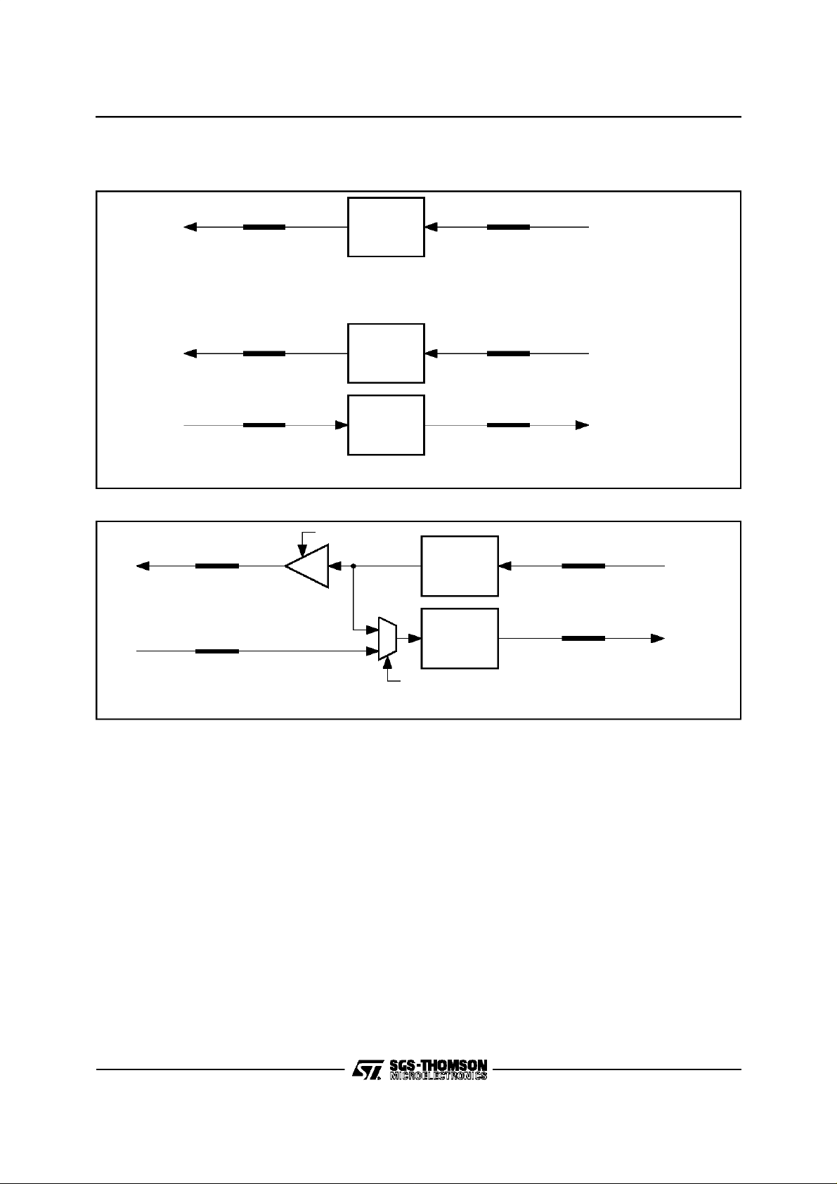
III.4- MicroprocessorInterface
III.4.1 - Description
The
Multi-HDLC
circuitcanbe controlledbysevera
typesof microprocessors(ST9,Intel/Motorola8 or
16 data bits interfaces) suchas :
- ST9family
- INTEL80C1888 bits
- INTEL80C18616 bits
- MOTOROLA68000 16 bits
During the initialization of the
Multi-HDLC
circuit,
themicroprocessorinterfaceisinformedof thetype
ofmicroprocessorthatisconnectedby polarisation
of three external pinsMOD 0/2).
TwochipSelect(CS0/1)pinsare provided.CS0will
select the internal registers and CS1 the external
memory.
0
16 Tx
C/I
1
2
3
4
5
6
7
D Cha nnels
to Rx HDLC
16 Tx
MON
SWITCHING
MATRIX
Internal Bus
Table14 : MicroprocessorInterfaceSelection
MOD2
MOD1
Pin
0 1 1 80C188
1 1 1 80C186
1 0 0 68000
0 0 0 Reserved
001 ST9
Pin
MOD0
Pin
Microprocessor
III.4.2 - Definitionof the Interface for the different microprocessors
Thesignalsconnectedtothe microprocessorinterface are presentedon thefollowing figures for the
different microprocessor (see Figures 12, 13, 14,
15, 16 and 17 on Pages 29-30).
5464-12.EPS
28/83
Page 29

III - FUNCTIONAL DESCRIPTION(continued)
Figure12 :
Multi-HDLC
connectedto µP with multiplexedbuses
MULTI-HDLC
PST9
µ
IINTEL
MOTOROLA
8/16 BITS
Figure13 :
Multi-HDLC
Multiplex
Address /Data Bus
connectedto µP with non-multiplexedbuses
P
µ
INTERFACE
Internal Bus
BUS ARBITRATION
MULTI-HDLC
µP
IINTEL
MOTOROLA
8/16 BITS
Figure14 : MicroprocessorInterfacefor INTEL80C188
Address Bus
Data Bus
µP
INTERFACE
Internal Bus
BUS ARBITRATION
RAM
INTERFACE
RAM
INTERFACE
Address Bus
Data Bus
Address Bus
Data Bus
STLC5464
STATIC or
DYNAMIC RAM
(organize d
by 16 bits)
5464-13.EPS
STATIC or
DYNAMICRAM
(organized
by 16bits)
5464-14.EPS
INT0/1 WDO
INTEL
80C188
ARDY
NWR
NRD
ALE
A8/19
AD0/7
Figure15 : MicroprocessorInterfacefor INTEL80C186
INT0/1 WDO
NBHE
INTEL
80C186
ARDY
NWR
NRD
ALE
A16/19
AD0/15
NRESET
CS0/1
NRESET
CS0/1
P
µ
INTERFACE
P
µ
INTERFACE
5464-15.EPS
5464-16.EPS
29/83
Page 30

STLC5464
III - FUNCTIONAL DESCRIPTION(continued)
Figure16 : MicroprocessorInterfacefor MOTOROLA68000
INT0/1 WDO
NRESET
CS0/1
NDTACK
MOTOROLA
68000
Figure17 : MicroprocessorInterfacefor ST9
INT0/1 WDO
R/NW
NUDS
NLDS
NAS
A1/23
AD0/15
NRESET
CS0/1
P
µ
INTERFACE
5464-15.EPS
ST9
WAIT
R/NW
NDS
NAS
A8/15
AD0/7
P
µ
INTERFACE
5464-19.EPS
30/83
Page 31

III - FUNCTIONAL DESCRIPTION(continued)
III.5- MemoryInterface
III.5.1 - Function Description
The memory interface allows the connection of
Static or Dynamic RAM. The memory space addressableinthetwo configurationsisnotthesame.
Inthe caseof dynamicmemory(DRAM),the memory interface will address up to 16 Megabytes.In
caseofstaticmemory(SRAM)only1Megabytewill
be addressed. The memory location is always organizedin 16 bits.
The memory is shared between the
Multi-HDLC
andthemicroprocessor.Theaccesstothe memory
is arbitrated by an internal function of the circuit:
the bus arbitration.
STLC5464
Example1: iftheapplicationrequires16bitmProcessorand 1 MegawordSharedmemorysize, three
capabilitiesare offered:
- 4 DRAM Circuits (256Kx16) or
- 4 DRAM Circuits (1Mx4) or
- 1 DRAM Circuit (1Mx16).
Example2 :if the applicationrequires8 bitmProc-
essorand 1 MegabyteSharedmemory size, three
capabilitiesare offered:
- 2 DRAM Circuits (256Kx16) or
- 8 SRAMCircuits (128Kx8)or
- 2 SRAMCircuits (512kx8).
Example3 : for small applicationsit is possible to
connect 2 SRAM Circuits (128Kx8) to obtain 256
Kilobytesshared memory.
III.5.2 - Choice of memoryversus microprocessorand capacityrequired
The memory interface depends on the memory
chips which are connected. As the memory chips
will be chosen versus the microprocessorand the
wanted memory space, the Table 22 presentsthe
differentconfigurations.
III.5.3 - MemoryCycle
For SRAM and DRAM, the different cycles are
programmable(see Paragraph”MemoryInterface
ConfigurationRegister MICR (32)H” on Page 71).
Each cycle is equal to : px 1/f
with f the frequencyof signalappliedto the Crystal
1 input and p selected by the user.
Table 22 : DRAM and SDRAM Selection versus µP
Microprocessor and
shared memory
8 bits
µProcessor
16 bits
µProcessor
DRAM Circuits proposed
Capacity Organization
4 Megabits 256Kx16 1(256Kx16) 2(256Kx16) 4(256Kx16)
16 Megabits 1Mx16 1(1Mx16) 2(1Mx16) 4(1Mx16)
64 Megabits 4Mx16 1(4Mx16) 2(4Mx16)
SRAM Circuits proposed
Capacity Organization
1 Megabits 128Kx8 4(128Kx8) 8(128Kx8)
4 Megabits 512kx8 2(512kx8)
Number of
Megabytes
Number of
Megawords
1Mx4 4(1Mx4) 8(1Mx4) 16(1Mx4)
4Mx4 4(4Mx4) 8(4Mx4)
0.5 1 2 4 8 16
0.25 0.5 1 2 4 8
Shared memory size required by the application
Not possible
31/83
Page 32

STLC5464
III - FUNCTIONAL DESCRIPTION(continued)
III.5.4 - SRAM interface
Signals A19 A18 A0 or equiv.
NCE7 1 1 1
NCE6 1 1 0
NCE5 1 0 1
NCE4 1 0 0
NCE3 0 1 1
NCE2 0 1 0
NCE1 0 0 1
NCE0 0 0 0
The SRAM space achieves 1 Mbyte max. It is
always organized in 16 bits. The structure of the
memoryplane is shownin the following figures.
Becauseof thedifferent chips usable, 19 address
wires and 8 NCE (Chip Enable) are necessary to
addressthe 1 Mbyte.TheNCEselectsthe Mostor
LeastSignificantByteversusthe valueof A0 delivered by theµP and the location of chip in the
memoryspace.
III.5.4.1- 18K x n SRAM
The Address bits delivered by the
Multi-HDLC
128Kx nSRAM circuits are :
ADM0/14 and ADM15/16 (17 bits) corresponding
withA1/17 deliveredby the µP.
Figure18 : 128K x 8 SRAM Circuit Memory
Organization
128K x 16
NCE 7
NCE 5
NCE 3
NCE 1
7
5
3
1
NCE 6
NCE 4
NCE 2
NCE 0
6
4
2
0
for
128K x 8
Figure19 : 512K x 8 SRAM CircuitMemory
Organization
512K x 16
512K x 8
NCE1
1
NCE0
DM8/15 DM0/7
0
III.5.5 - DRAM Interface
In DRAM, thememoryspacecan achieveup to 16
megabytes organized by 16 bits. Eleven address
wires, four NRAS and two NCAS are needed to
select any byte in the memory. One NRAS signal
selects1 bankof 4andtheNCASsignalsselectthe
bytes concernedby the transfer (1 or 2selectinga
byte or a word). The DRAM memory interface is
then defined. The ”RAS only” refresh cycles will
refresh all memory locations. The refresh is programmable. The frequency of the refresh is fixed
by the memoryrequirements.
III.5.5.1- 256Kx n DRAM Signals
Signals A20 A19 A0 or equiv.
NRAS3 1 1
NRAS2 1 0
NRAS1 0 1
NRAS0 0 0
NCAS1 1
NCAS0 0
The Address bits delivered by the
Multi-HDLC
for
256K x n DRAMcircuitsare :
ADM0/8(2 x9 = 18bits)correspondingwithA1/18
deliveredby theµP.
Figure 20 : 256Kx 16 DRAMCircuit Organization
CAS1 CAS0
256K x 16
RAS3
7
6
5464-21.EPS
DM8/15 DM0/7
III.5.4.2- 512K x n SRAM
Signals A0 or equiv.
NCE1 1
NCE0 0
The Address bits delivered by the
Multi-HDLC
for
512Kx nSRAM circuits are :
ADM0/14 and ADM15/18 (19 bits) corresponding
withA1/19 deliveredby the µP.
32/83
5464-20.EPS
RAS2
RAS1
RAS0
ADM0/8, NWE, NOE a re connecte d to e a ch circuit.
5
3
1
DM8/15 DM0/7
4
2
0
5464-22.EPS
Page 33

III - FUNCTIONAL DESCRIPTION(continued)
III.5.5.2- 1M x nDRAM Signals
STLC5464
Figure22 : 4Mx 16 DRAM CircuitOrganization
Signals A22 A20 A0 or equiv.
NRAS3 1 1
NRAS2 1 0
NRAS1 0 1
NRAS0 0 0
NCAS1 1
NCAS0 0
The Address bits delivered by the
Multi-HDLC
for
1M x n DRAM circuits are :
ADM0/9(2x10 =18bits)correspondingwithA1/20
deliveredby theµP.
Figure21 : 1Mx 16 DRAM Circuit Organization
NCAS1 NCAS0
1M x 16
NRAS3
NRAS2
NRAS1
NRAS0
ADM0/9, NWE, NOE are connected to e a c h circuit
7
5
3
1
DM8/15 DM0/7
6
4
2
0
NCAS1 NCAS0
4M x 16
NRAS1
NRAS0
ADM0/10, NWE, NOE a re connected to e a ch circuit
3
1
DM8/15 DM0/7
2
0
III.6 - Bus Arbitration
The Bus arbitration function arbitrates the access
to the bus between different entities of thecircuit.
Those entities which can call for the bus are the
following:
- The receive DMAcontroller,
- The microprocessor,
- The transmit DMA controller,
- The Interrupt controller,
- The memory interfacefor refreshing the DRAM.
This list gives the memory access priorities per
default.
If the treatmentof morethan 32 HDLC channelsis
required by the application, it is possible to chain
several
Multi-HDLC
components.Thatis done with
two external pins (TRI, TRO) and a token ring
system.
The TRI, TRO signals are managed by the bus
arbitration function too. When a chip has finished
its tasks,it sendsa pulse of 30ns to thenext chip.
Figure 23 : Chainof n
5464-23.EPS
Multi-HDLC
Components
5464-24.EPS
III.5.5.3- 4M x nDRAM Signals
Signals A23 A0 or equiv.
NRAS1 1
NRAS0 0
NCAS1 1
NCAS0 0
The Address bits delivered by the
Multi-HDLC
for
4M x n DRAM circuits are :
ADM0/10 (2 x 11 = 22 bits) corresponding with
A1/22delivered by theµP.
TRI
P
µ
P Bus RAMBus
µ
MHDLC 0
TRO
TRI
MHDLC 1
TRO
TRI
MHDLC n
TRO
RAM
5464-25.EPS
33/83
Page 34

STLC5464
III - FUNCTIONAL DESCRIPTION(continued)
III.7- Clock Selectionand TimeSynchronization
III.7.1 - Clock DistributionSelection
and Supervision
Two clock distributions are available : Clock at
4.096MHzor8.192MHzand asynchronizationsignal at 8kHz. The component has to select oneof
these two distributions and to check its integrity
(seeFigure25 andParagraph”GeneralConfigurationRegister GCR (02)H”on Page 57).
DCLK, FSCGCI and FSCV* are output on three
externalpins ofthe
selected between Clock A and Clock B. FSCGCI
and FSCV* are functions of the selected distribution and respect the GCI and V* frame synchronizationspecifications.
Thesupervisionof theclockdistributionconsists of
verifyingits availability. The detectionof the clock
absence is done in less than 250µs. In case the
clock is absent, an interrupt is generated with a
4kHz recurrence. Then the clock distribution is
switched by the microprocessor. This change of
clockoccurs on a falling edge of thenew selected
distribution.
Figure24 : MHDLCClock Generation
Multi-HDLC
. DCLKis the clock
Dependingon the applications,three different signals of synchronization (GCI, V* or Sy) can be
provided to the component. The clock A/B frequency can be a 4096 or 8192kHz clock. The
componentis informed of thesynchronizationand
clocksthat are connectedby software.Thetimings
of thedifferentsynchronizationare given Page38.
III.7.2 - VCXOFrequency Synchronization
An external VCXOcan be used to providea clock
to thetransmissioncomponents.Thisclock is controlled by the main clock distribution (Clock A or
ClockB at 4096kHz). As the clock of the transmission componentis 15360or 16384kHz,a configurable functionis necessary.
The VCXO frequencyis divided by P (30 or32) to
provide a common sub-multiple (512kHz) of the
reference frequency CLOCKA or CLOCKB
(4096kHz). The comparison of these two signals
gives an error signal which commands the VCXO.
Twoexternal pinsare needed to performthis function : VCXO-INand VCXO-OUT(seeFigure 26 on
Page 35).
REF. CLOCK RESET INT1
(CSD)
Clock Lack
Detection
from 250µs
HCLClock
Frame
Clock
CLOCK
ADAPTATION
SYN0SYN1
To the internal
FSCGCI
DCLK
MHDLC
FRAME A
CLOCKA FS CV*
CLOCK SELECTION
FRAME B
CLOCKB
SelectA or B
(SELB)
At RESET
FRAME A and CLOCK A
are selected
Supervision
Deactivation
AorB
Selected
(BSEL)
GENERAL CONFIGURATION REGISTER (GCR)
5464-26.EPS
34/83
Page 35

III - FUNCTIONAL DESCRIPTION(continued)
Figure25 : VCXOFrequencySynchronization
STLC5464
VCXO
f = 15360kHz
or 16384kHz
VCXO IN
iff = 153 60kHz, p = 30
iff = 163 84kHz, p = 32
7
4096kHz
III.8- InterruptController
III.8.1 - Description
Threeexternal pins are used to managethe interruptsgenerated by the
Multi-HDLC
. The interrupts
have three main sources :
- The operating interrupts generatedby the HDLC
receivers/transmitters, the CI receivers and the
monitor transmitters/receivers. INT0 Pin is reserved for this use.
- The interrupt generatedbyan abnormalworking of
theclockdistribution.INT1Pinisreservedforthisuse.
- The non-activity of the microprocessor (Watch-
dog). WDO Pin is reservedfor thisuse.
III.8.2 - Operating Interrupts (INT0 Pin)
Thereare five mainsourcesof operatinginterrupts
in the
Multi-HDLC
circuit:
- The HDLC receiver,
- The HDLC transmitter,
- The CI receiver,
- The Monitor receiver,
- The Monitor transmitter.
When an interrupt is generated by one of these
functions,the interrupt controller :
- Collectsall the informationabout the reasons of
this interrupt,
- Storesthem in externalmemory,
- Informs the microprocessor by positioning the
INT0 pin in the high level.
Threeinterruptqueuesarebuiltinexternalmemory
to store the informationabout the interrupts :
- Asinglequeuefor the HDLCreceiversandtrans-
mitters,
- Onefor the CI receivers,
- Onefor the monitor receivers.
The microprocessor takes the interrupts into ac-
count by reading the Interrupt Register (IR) of the
interruptcontroller.
LOW P ASS
FILTER
/p
OUX
/8
8
VCXO OUT
EVMMHDLCRef =
This register informs the microprocessor of the
interrupt source. The microprocessor will have informationabout the interruptsourceby readingthe
correspondinginterruptqueue (seeParagraph”InterruptRegister IR (38)
” on Page 74).
H
Onan overflowof the circularinterruptqueuesand
an overrun or underrun of the different FIFO, the
INT0 Pinis activatedand the originof theinterrupt
is storedin theInterruptRegister.
A16 bits register is associatedwith the Tx Monitor
interrupt. It informs the microprocessor of which
transmitterhas generatedthe interrupt (see Paragraph ”Transmit Monitor Interrupt Register TMIR
” on Page 71).
(30)
H
III.8.3 - TimeBase Interrupts (INT1 Pin)
The Time base interrupt is generated when an
absence or an abnormalworking of clock distribution is detected.The INT1 Pin is activated.
III.8.4 - EmergencyInterrupts (WDO Pin)
The WDO signal is activatedby an overflow of the
watchdogregister.
III.8.5 - InterruptQueues
There are three different interruptqueues :
- Tx and Rx HDLCinterruptqueue,
- Rx C/I interruptqueue,
- Rx Monitor interrupt queue.
Their length can be defined by software.
For debugging function,each interrupt word of the
CI interruptqueueand monitorinterruptqueuecan
befollowedbya timestampedword.Itiscomposed
of a counterwhich runs in therange of 250µs.The
counter is the same as the watchdog counter.
Consequently,thewatchdogfunctionisn’tavailable
at thesame time.
5464-27.EPS
35/83
Page 36

STLC5464
III - FUNCTIONAL DESCRIPTION(continued)
Figure26 : TheThree CircularInterruptMemories
IBA
INITIALIZATION
BLOCK
IBA+ 254
IBA+ 256
HDLC (Tx a nd Rx)
INTERRUPTQUE UE
III.9- Watchdog
This functionis used to controlthe activity of the
application. It is composed of a counter which
counts down from an initial value loaded in the
Timerregister by the microprocessor.
If the microprocessor doesn’t reset this counter
before it is totally decremented, the external Pin
WDOis activated; this signal can be usedto reset
the microprocessorand all the application.
Theinitial timevalue of the counteris programmable from 0 to15s in incrementsof 0.25ms.
Atthe reset of the component,the counteris automaticallyinitialized by the value corresponding to
512ms which are indicated in the Timer register.
IBA+ 256
+ HDLC
Queue Size
MON (Rx)
INTERRUP TQUEUE
IBA+ 256
+ HDLC
Queue S ize
+ MON
Queue S ize
C/I (Rx)
INTERRUP TQUE UE
The microprocessormust put WDR (IDCR Register) to”1”to reset this counter and to confirmthat
the applicationstarted correctly.
In the reverse case,the WDOsignalcouldbeused
to reset the board a secondtime.
III.10 - Reset
There are two possibilities to resetthe circuit :
- by software,
- by hardware.
Each programmable register receives its default
value. After that, the default value of each data
registeris storedin the associatedmemory except
for Time slot Assigner memory.
5464-28.EPS
36/83
Page 37

STLC5464
IV- DC SPECIFICATIONS
AbsoluteMaximumRatings
Symbol Parameter Value Unit
V
T
PowerDissipation
Symbol Parameter Test Conditions Min. Typ. Max. Unit
Recommended DC Operating Conditions
Symbol Parameter Test Conditions Min. Typ. Max. Unit
V
T
Note 1 : All the following specifications are valid only within these recommended operating conditions.
TTL Input DC ElectricalCharacteristics
Symbol Parameter Test Conditions Min. Typ. Max. Unit
V
V
I
Vhyst SchmittTrigger hysteresis 0.4 0.7 1 V
VT+ Positive Trigger Voltage 2 2.4 V
VT- Negative Trigger Voltage 0.6 0.8 V
C
C
C
Note 2 : Excluding package
5V Power Supply Voltage -0.5, 6.5 V
DD
Input or Output Voltage -0.5, V
Storage Temperature -55, +125 °C
stg
P Power Consumption V
5V Power Supply Voltage 4.75 5.25 V
DD
Operating Temperature 0 +70 °C
oper
Low Level Input Voltage 0.8 V
IL
High Level Input Voltage 2.0 V
IH
Low Level Input Current VI=0V 1 µA
I
IL
High Level Input VI=V
IH
Input Capacitance (see Note 2) f = 1MHz@ 0V 2 4 pF
IN
Output Capacitance 4
OUT
Bidirextional I/O Capacitance 4 8
I/O
= 5V 400 mW
DD
DD
+ 0.5 V
DD
-1
A
µ
CMOSOutput DC ElectricalCharacteristics
Symbol Parameter Test Conditions Min. Typ. Max. Unit
V
V
Note 3 : X is the source/sink current under worstcase conditions and is reflected in thename of the I/O cell according to thedrive capability.
Low Level Output Voltage IOL= X mA (see Note 3) 0.4 V
OL
High Level Output Voltage IOH= -X mA (see Note 3) V
OH
X = 4 or 8mA.
-0.4 V
DD5
Protection
Symbol Parameter Test Conditions Min. Typ. Max. Unit
VESD Electrostatic Protection C = 100pF, R = 1.5k
Ω
2000 V
37/83
Page 38

STLC5464
V - CLOCKTIMING
V.1 - SynchronizationSignals deliveredby the system
For one of three different input synchronizations which is programmed, FSCG and FSCV* signals
deliveredby the
Figure27 :
CLOCK B
Multi-HDLC
are in accordancewith the figure hereafter.
Clocksreceivedand deliveredby the
Multi-HDLC
CLOCK A
1) Sy Mod e
Frame A(or B)
2) GCIMode
Frame A(or B)
3) V*Mode
Frame A(or B)
DIN 0/8, ECHO
DOUT 0/7, CB
if FS = FSCG
TDM0/7
delivered
FSCG
by the circuit
t5ht2 t5l
4536701
Bit4 Bit5 Bit0 Bit1Bit6 Bit7Bit3
Time Slot 31 Time S lot 0
t1
t4t3t4t3
t3
t4 CGI
delivered
FSCV*
by the circuit
The four Multiplex Configuration Registers are at zero (no delay).
Symbol Parameter Min. Typ. Max. Unit
t1 Clock Period if 4096kHz
Clock Period if 8192kHz
t2 Delay between Clock A and Clock B - 60 0 +60 ns
t3 Set uptime FrameA (orB)/CLOCK A(or B) 10 t1-10 ns
t4
t4GCI
38/83
Hold time Frame A(or B)/CLOCK A(or B) 10
t5 Clock ratio t5h/t5l 75 100 125 %
239
120
10
244
122
125000 - (t1 - 10)
249
125
t1-10
5464-29.EPS
ns
ns
ns
Page 39

V - CLOCKTIMING (continued)
V.2 - TDM Synchronization
Figure28 : SynchronizationSignals receivedby the
CLOCK A (o r B)
STLC5464
Multi-HDLC
t2
DCLK de live red by
the Multi-HDLC
delivered by
FSCG
the Multi-HDLC
DOUT0/7, CB
Bit 7, Time S lot 31
DIN0/8
ECHO
The four Multiplex Configura tion Re gisters a re a tzero (no delay betwe en FS and Multiplexes).
t1
t3
t6
t4
t5
Bit 0, Time Slot 0
t7t7
t9
t8
Symbol Parameter Min. Typ. Max. Unit
t1 Clock Period if 4096kHz
Clock Period if 2048kHz
Id CLOCKA or B 244
488
Id CLOCKA or B ns
ns
t2 Delay between CLOCK A or B and DCLK (30pF) 5 30 ns
t3 Set-up Time FS/DCLK 20 t1-20 ns
t4 Hold Time FS/DCLK 20 ns
t5 Duration FS 244 125000-244 ns
t6 DCLK to Data 50pF
DCLK to Data 100pF
50
100
ns
t7 Set-up Time Data/DCLK 20 ns
t7 Hold Time Data/DCLK 20 ns
t8 Set-up Echo/DCLK (rising edge) 155 ns
t9 Hold Time Echo/DCLK (rising edge) 205 ns
5464-30.EPS
39/83
Page 40

STLC5464
V - CLOCKTIMING (continued)
V.3 - GCI Interface
Figure29 : GCISynchroSignal delivered by the
received by
FS
the Multi-HDLC
CH0 CH1 CH7
DIN4/5
DOUT4/5
Multi-HDLC
125µs
GCI Ch ann e l
DCLK de livered by
the Multi-HDLC
de live red by
FS CG
the Multi-HDLC
DOUT0/7, CB
if FSCG is connected to FS
DIN0/8
The four Multiplex Configuration Registers are at zero (no delay between FS and Multiplexes).
B1 B2 MON D C/I AE
t1
t3
t6
Bit 0, Time Slot 0
t3
t7t7
Symbol Parameter Min. Typ. Max. Unit
t1 Clock Period if 4096kHz
Clock Period if 2048kHz
CLOCKA/B Tmin 244
488
CLOCKA/B Tmax ns
ns
t3 DCLK to FSCG 20 ns
t5 Duration FS 244 125000-244 ns
t6 DCLK to Data 50pF
DCLK to Data 100pF
50
100
ns
ns
t7 Set-up Time Data/DCLK 20 ns
t7 Hold Time Data/DCLK 20 ns
5464-31.EPS
40/83
Page 41

V - CLOCKTIMING (continued)
V.4 - V* Interface
Figure30 : V*SynchronizationSignaldelivered by the
FS re ceived by
the Multi-HDLC
CH0 CH1 CH7
DIN4/5
DOUT4/5
STLC5464
Multi-HDLC
125µs
GCI Cha nn e l
de livered by
DCLK
the Multi-HDLC
delivered by
FSCV*
the Multi-HDLC
DOUT0/7, CB
ifF SC G is con necte d to FS
DIN0/8
The four Multiple x Configuration Registers a re at zero (no delay be twee n FS and Multiplexes).
Symbol Parameter Min. Typ. Max. Unit
t1 Clock Period 4096kHz 244 ns
t3 DCLK to FSCV* 20 ns
t5 Duration FSCV* 244 ns
t6 Clock to Data 50pF
Clock to Data 100pF
t7 Set-up Time Data/DCLK 20 ns
t7 Hold Time Data/DCLK 20 ns
B1 B2 MON D C/I AT
t1
t3
Bit 3, Time Slot 31
t3
t7t7
50
100
ns
nS
5464-32.EPS
41/83
Page 42

STLC5464
VI- MEMORYTIMING
VI.1- Dynamic Memories
Figure31 : DynamicMemory Read Signals fromthe
Multi-HDLC
NDS fromµP
(or equiva lent)
MASTERCLOCK
applied to XTAL1 Pin
NRAS0/3
NCAS0/1
NWE
ADM0/10
NOE
DM0/15
DRAMCircuit
Note :
MBLDefinition
from
See
T Total Rea d Cycle
aaa
HZ HZ
Tu
Tv
Tv/2
Each signal from the MHDLC is high
impedance outside this time ifMBL= 0
Tw Tz
Tw + Tz/2
Ts
aa
a
Th
1/f
HZHZ
Symbol Parameter Min. Typ. Max. Unit
T Delay between Data Strobe from the mP and beginning of cycle 2/f
a Delay between Masterclock andEdge of each signaldelivered by the
20 ns
MHDLC (30pF)
Tw Delay between NCAS Falling Edge and NCAS risingEdge 1/f 2/f ns
Tz Delay between NCAS Rising Edgeand end of cycle 1/f 2/f ns
Ts Set-up Time Data /NCAS Rising Edge 20 ns
Th Hold Time Data/NCAS Rising Edge 0 ns
5464-33.EPS
42/83
Page 43

VI- MEMORYTIMING (continued)
Figure32 : DynamicMemory Write Signals from the
STLC5464
Multi-HDLC
NDS from µP
(or equivalent)
MASTERCLOCK
applied to XTAL1 P in
NRAS0/3
NCAS0/1
NWE
ADM0/10
DM0/15
NOE
Note : See
MBLDefinition
T Total Write Cycle
aaa
HZ HZ
Tu
Tv
Tv/2
Td
Ea ch signal from the MHDLC is high
impedance outside this time if MBL= 0
Tw Tz
aa
a
1/f
HZHZ
Symbol Parameter Min. Typ. Max. Unit
1/f f : Masterclock Frequency 32 33 MHz
Tu Delay between beginning of cycle and NRAS Falling Edge 1/f 2/f ns
Tv Delay between NRAS Falling Edge and NCAS Falling Edge 1/f 2/f ns
Tw Delay between NCAS Falling Edge and NWE Rising Edge 1/f 2/f ns
Tz Delay between NWE Rising Edge and end ofcycle 1/f 2/f ns
Tv/2 Delay between NRAS Falling Edge andaddresschange 1/2f 1/f ns
Td Data Valid after beginning of cycle(30 pF) 1/f 1/f ns
Note : TotalCycle : Tu+ Tv+ Tw+ Tz
5464-34.EPS
43/83
Page 44

STLC5464
VI- MEMORYTIMING (continued)
VI.2- StaticMemories
Figure33 : StaticMemory Read Signals from the
Multi-HDLC
NDS from µP
(or equivalent)
MASTERCLOCK
applied to XTAL1Pin
ADM0/18
NCE0/7
NWE
NOE
DM0/15
SRAM Circuit
Note :
MBLDefinition
from
See
T Total Read Cycle
aa
a
HZ HZ
Twz
Each signal delivered by the MHDLC
is high impedance outside this time
a
HZHZ
Ts Th
1/f
Symbol Parameter Min. Typ. Max. Unit
T Delay between Data Strobe delivered by the mP and beginning of
2/f
cycle
1/f f: Masterclock frequency
Total read cycle: Twz + 1/f
a Delay between Masterclock andEdge of each signaldelivered by the
20 ns
MHDLC (30pF)
Twz NOE width 1/f 4/f ns
Ts Set-up Time Data /NOE Rising Edge 20 ns
Th Hold Time Data /NOE Rising Edge 0 1/f ns
5464-35.EPS
44/83
Page 45

VI- MEMORYTIMING (continued)
Figure34 : StaticMemory Write Signals from the
STLC5464
Multi-HDLC
NDS from µP
(or equivalent)
MASTERCLOCK
appliedto XTAL1Pin
ADM0/18
NCE0/7
NWE
NOE
DM0/15
Note : See
MBL Definition
T Total Write Cycle
a
a
HZ HZ
Tuv
Each signal delivered by the MHDLC
is high impedance outside this time
aa
a
1/f
HZHZ
Symbol Parameter Min. Typ. Max. Unit
T Delay between Data Strobe delivered by theµP and beginning of
2/f
cycle
1/f f : Masterclock frequency
a Delay between Masterclock andEdge of each signaldelivered by the
20 ns
MHDLC (30pF)
Tuv NCE width 1/f 4/f ns
Note : TotalWrite Cycle : Tuv + 1/f
5464-36.EPS
45/83
Page 46

STLC5464
VII - MICROPROCESSORTIMING
VII.1- ST9Family MOD0=1, MOD1=0, MOD2=0
Figure35 : ST9Read Cycle
NCS0/1
t1 t2
READY
NAS/
ALE
t4
t3
t12
t11
NDS/NRD
t7 t8
D0/7
AD0/7
t6t5
A0/7
t10
NWR
R/W /
Symbol Parameter Min. Typ. Max. Unit
t1 Delay Ready / Chip Select (if t3 > t1), (30pF) 0 30 ns
t2 Hold Time Chip Select /DataStrobe 14 ns
t3 Delay Ready / NAS (if t1 > t3), (30pF) 0 30 ns
t4 WidthNAS 20 ns
t5 Set-up Time Address / NAS 9 ns
t6 Hold Time Address / NAS 9 ns
t7 Data Valid before Ready 0 ns
t8 Data Valid after Data Strobe (30pF) 0 ns
t9 Set-up Time R/W /NAS 15 ns
t10 Hold Time R/W / Data Strobe 15 ns
t11 Width NDS when immediate access 50 ns
t12 Delay NDS / NCS 5 ns
t9
5464-37.EPS
46/83
Page 47

VII - MICROPROCESSORTIMING (continued)
Figure36 : ST9Write Cycle
NCS0/1
STLC5464
t1 t2
READY
ALE
NAS/
t4
t3
t12
t11
NDS/NRD
t7
t8
AD0/7
A0/7
t6t5
D0/7
t10t9
R/W /
NWR
Symbol Parameter Min. Typ. Max. Unit
t1 Delay Ready / Chip Select (if t3 > t1), (30pF) 0 30 ns
t2 Hold Time Chip Select / Data Strobe 14 ns
t3 Delay Ready / NAS (if t1 > t3), (30pF) 0 30 ns
t4 WidthNAS 20 ns
t5 Set-up Time Address / NAS 9 ns
t6 Hold Time Address / NAS 9 ns
t7 Set-up Time Data / Data Strobe -15 ns
t8 Hold Time Data / Data Strobe 15 ns
t9 Set-up Time R/W / NAS 15 ns
t10 Hold Time R/W / Data Strobe 15 ns
t11 Width NDS when immediate access 50 ns
t12 Delay NDS / NCS 5 ns
5464-38.EPS
47/83
Page 48

STLC5464
VII - MICROPROCESSORTIMING (continued)
VII.2- 80C188MOD0=1, MOD1=1,MOD2=0
Figure37 : 80C188Read Cycle
NCS0/1
READY
t3
t1 t2
NAS/ALE
NDS/NRD
AD0/7
t4
t12
t6t5
A0/7
t7 t8
D0/7
R/W / NWR
Symbol Parameter Min. Typ. Max. Unit
t1 Delay Ready / Chip Select (if t3 > t1), (30pF) 0 20 ns
t2 Hold Time Chip Select / NRD 10 ns
t3 Delay Ready / ALE (if t1 > t3),(30pF) 0 20 ns
t4 WidthALE 20 ns
t5 Set-up Time Address / ALE 5 ns
t6 Hold Time Address / ALE 5 ns
t7 Data Valid before Ready 0 ns
t8 Data Valid after NRD (30pF) 0 ns
t12 Delay NDS / NCS 0 ns
5464-39.EPS
48/83
Page 49

VII - MICROPROCESSORTIMING (continued)
Figure38 : 80C188Write Cycle
NCS0/1
READY
t3
STLC5464
t1 t2
NAS/ALE
NDS/NRD
AD0/7
R/W / NWR
Symbol Parameter Min. Typ. Max. Unit
t1 Delay Ready / Chip Select (if t3 > t1), (30pF) 0 20 ns
t2 Hold Time Chip Select / NWR 10 ns
t3 Delay Ready / ALE (if t1 > t3),(30pF) 0 20 ns
t4 WidthALE 20 ns
t5 Set-up Time Address / ALE 5 ns
t6 Hold Time Address / ALE 5 ns
t7 Set-up Time Data / NWR -15 ns
t8 Hold Time Data / NWR 15 ns
t12 Delay NWR / NCS 0 ns
t4
A0/7
t6t5
t12
D0/7
t8
t7
5464-40.EPS
49/83
Page 50

STLC5464
VII - MICROPROCESSORTIMING (continued)
VII.3- 80C186MOD0=1, MOD1=1,MOD2=1
Figure39 : 80C186Read Cycle
NCS0/1
READY
t3
t1 t2
NAS/ALE
NDS/NRD
AD0/15
t4
t12
t5
A0/15
t6
t7 t8
D0/15
R/W / NWR
t10
NBHE
NBHE A16/19
t9 t11
NBHE
A16/19
Symbol Parameter Min. Typ. Max. Unit
t1 Delay Ready / Chip Select (if t3 > t1), (30pF) 0 20 ns
t2 Hold Time Chip Select / NRD 10 ns
t3 Delay Ready / ALE (if t1 > t3),(30pF) 0 20 ns
t4 WidthALE 20 ns
t5 Set-up Time Address / ALE 5 ns
t6 Hold Time Address / ALE 5 ns
t7 Data Valid before Ready -15 ns
t8 Data Valid after NRD (30pF) 0 ns
t9 Set-up Time NBHE-Address A16/19 / ALE 5 ns
t10 Hold Time Address A1619 / NRD 10 ns
t11 Hold Time NBHE-/ NRD 10 ns
t12 Delay NRD / NCS 0 ns
5464-41.EPS
50/83
Page 51

VII - MICROPROCESSORTIMING (continued)
Figure40 : 80C186Write Cycle
NCS0/1
READY
t3
STLC5464
t1 t2
NAS/ALE
NDS/NRD
AD0/15
R/W / NWR
NBHE A16/19
t4
t5
A0/15
t6
D0/15
t12
t8
t7
t9 t11
NBHE
A16/19
t10
NBHE
Symbol Parameter Min. Typ. Max. Unit
t1 Delay Ready / Chip Select (if t3 > t1), (30pF) 0 20 ns
t2 Hold Time Chip Select / NWR 10 ns
t3 Delay Ready / ALE (if t1 > t3),(30pF) 0 20 ns
t4 WidthALE 20 ns
t5 Set-up Time Address / ALE 5 ns
t6 Hold Time Address / ALE 5 ns
t7 Set-up Time Data / NWR -15 ns
t8 Hold Time Data / NWR 15 ns
t9 Set-up Time NBHE-Address A16/19 / ALE 5 ns
t10 Hold Time Address 16/19 / ALE 10 ns
t11 Hold Time NBHE-/ NWR 10 ns
t12 Delay NWR / NCS 0 ns
5464-42.EPS
51/83
Page 52

STLC5464
VII - MICROPROCESSORTIMING (continued)
VII.4- 68000MOD0=0, MOD1=0,MOD2=1
Figure41 : 68000Read Cycle
NCS0/1
t1 t2
NDTACK
NAS/
ALE
SIZE0/NLDS
SIZE1/NUDS
A1/23
R/W /
NWR
t12
t3
t5
A1/23
t7
t4
t6
t8
D0/15
Symbol Parameter Min. Typ. Max. Unit
t1 Delay NDTACK / NCS0/1 (if t3 > t1), (30pF)
Delay when immediate access
t2 Hold Time Chip Select / NLDS-NUDS 14 ns
t3 Delay NDTACK / NLDS-NUDS FallingEdge (ift1> t3), (30pF)
Delay when immediate access
t4 Delay NDTACK / NLDS-NUDS Rising Edge 0 30 ns
t5 Set-up Time Address / NAS 9 ns
t6 Hold Time Address / NLDS-NUDS 9 ns
t7 Data Valid before NDTACK FallingEdge (30pF) 0 ns
t8 Data Valid after NLDS-NUDS Rising Edge (30pF) 0 ns
t12 Delay NDS / NCS 0 ns
0
30
0
30
ns
ns
ns
ns
5464-43.EPS
52/83
Page 53

VII - MICROPROCESSORTIMING (continued)
Figure42 : 68000Write Cycle
NCS0/1
STLC5464
t1 t2
NDTACK
ALE
NAS/
/NLDS
SIZE0
SIZE1/NUDS
A1/23
NWR
R/W /
t12
t3
t5
A1/23
t9
t4
t6
t10
D0/15
Symbol Parameter Min. Typ. Max. Unit
t1 Delay NDTACK / NCS0/1 (if t3 > t1), (30pF)
Delay when immediate access
t2 Hold Time Chip Select / NLDS-NUDS 14 ns
t3 Delay NDTACK / NLDS-NUDS FallingEdge (ift1> t3), (30pF)
Delay when immediate access
t4 Delay NDTACK / NLDS-NUDS Rising Edge ns
t5 Set-up Time Address / NAS 9 ns
t6 Hold Time Address / NLDS-NUDS 9 ns
t9 Set-up Time Data / NLDS-NUDS 15 ns
t10 Hold Time Data / NLDS-NUDS 15 ns
t12 Delay NDS / NCS 0 ns
0
30
0
30
ns
ns
ns
ns
5464-44.EPS
53/83
Page 54

STLC5464
VII - MICROPROCESSORTIMING (continued)
VII.5- Token Ring Timing
Figure43 : TokenRing
MASTER CLOCK
(applied to XTAL1 Pin)
a
TRO
1/f
a
t
S
t
H
TRI
Symbol Parameter Min. Typ. Max. Unit
1/f f : Masterclock frequency 32.768 MHz
a Delay between Masterclock RisingEdge and Edges of TRO Pulse
25 ns
delivered by the MHDLC (10pF)
t
Set-up Time TRI/Masterclock Masterclock Falling Edge 5 ns
S
Hold Time TRI/Masterclock Falling Edge 5 0 ns
t
H
VII.6- MasterClock Timing
Figure44 :
Symbol Parameter Min. Typ. Max. Unit
f Masterclock Frequency 30 32.768 33 MHz
1/f Masterclock Period 30.3 30.5 33.3 ns
tH Masterclock High 12 ns
tL Masterclock Low 12 ns
MasterClock
MASTER CLOCK
(applied to XTAL1 Pin)
1/f
t
H
t
L
5464-47.EPS
5464-48.EPS
54/83
Page 55

STLC5464
VIII - INTERNALREGISTERS
‘Not used’ bits (Nu)are accessible by the microprocessor but the use of these bitsby software is not
recommended.
‘Reserved’bits are not implemented in thecircuit. However,it is not recommendedto usethis address.
VIII.1 - Identification and Dynamic Command Register - IDCR (00)H
bit15 bit8 bit7 bit 0
C15 C14 C13 C12 C11 C10 C9 C8 C7 C6 C5 C4 C3 C2 C1 C0
Whenthis register is read by the microprocessor, the circuit code C0/15 is returned.Reset has no effect
on this register.
C0/3indicates the version.
C4/7indicates the revision.
C8/11indicates the foundry.
C12/15indicates the type.
Example: this code is (0010)H for thefirst sample.
Whenthis register is written by the microprocessorthen :
bit15 bit8 bit7 bit 0
Nu Nu Nu Nu Nu Nu Nu Nu Nu Nu Nu Nu Nu RSS WDR TL
TL : TOKENLAUNCH
WhenTLis set to1 by the microprocessor,thetoken pulse is launchedfrom theTROpin (Token
RingOutput pin). This pulse is providedto theTRI pin(Token Ring Input pin)of thenext circuit
in the applicationswhere several
Multi-HDLC
WDR : WATCHDOG RESET.
Whenthe bit 1 (WDR)of this registeris set to 1 by the microprocessor, thewatchdogcounter is
reset.
RSS : RESET SOFTWARE
Whenthe bit 2 (RSS)of this register is setto 1 by themicroprocessor,the circuitis reset(Same
actionas reset pin).
Afterwriting this register,the values of these three bits return to thedefaultvalue.
s are connectedto the same shared memory.
VIII.2 - GeneralConfiguration - GCR(02)H
bit15 bit8 bit7 bit 0
Nu MBL AFAB SCL BSEL SELB CSD HCL SYN1 SYN0 D7 EVM TSV TRD PMA WDD
After reset (0000)
H
WDD : Watch DogDisable
WDD = 1, the WatchDog is masked : WDO pin stays at ”0”.
WDD= 0, the WatchDog generatesan ”1”on WDO pin if the microprocessorhas not reset the
WatchDog during the duration programmed in Timer Register.
PMA : Priority Memory Access
PMA = 1, if the token ring has been launched it is captured and kept in order to authorize
memoryaccesses.
PMA= 0, memoryis accessibleonly if the token is present;after one memory access the token
is re-launched from TRO pin of thecurrent circuit to TRI pin ofthe next circuit.
TRD : TokenRing Disable
TRD = 1, if the token has been launched, the token ring is stoppedand destroyed ; memory
accessesare not possible.The token will not appear on TROpin.
TRD= 0,thetokenringisauthorized; whenthetokenwillbelaunched,it will appearonTROpin.
55/83
Page 56

STLC5464
VIII - INTERNALREGISTERS(continued)
TSV : TimeStampingValidated
TSV= 1,the timestampingcounterbecomesa freebinarycounterand countsdownfrom65535
to0 in step of 250ms(Total = 16384ms).So if anevent occurswhenthe counterindicatesAand
if the nextevent occurs when the counterindicatesB then : t = (A-B)x 250ms is thetime which
haspassedbetweenthetwoeventswhichhavebeenstoredinmemorybytheInterruptController
(forRx C/Iand RxMON CHANNELonly).
TSV = 0, the counter becomes a decimalcounter.TheTimer Registerand this decimal counter
constitutea WatchDog or aTimer.
EVM : EXTERNAL VCXO MODE
EVM=1,VCXOSynchronizationCounter is divided by 32.
EVM=0,VCXOSynchronizationCounter is divided by 30.
D7 : HDLC connectedto MATRIX
D7 = 1, the transmit HDLC is connected to matrix input 7, theDIN7 signal isignored.
D7 = 0, the DIN7 signal is taken into accountby the matrix, the transmitHDLC is ignoredby the
matrix.
SYN0/1: SYNCHRONIZATION
SYN0/1 : these two bits define the signal applied on FRAMEA/Binputs. For more details, see
”Synchronizationsignals delivered by the system. 7.1.
SYN1 SYN0 Signal applied on FRAMEA/B inputs
0 0 SYIinterface
0 1 GCI Interface (the signaldefines the first bit of the frame)
1 0 Vstar Interface (the signal defines thridbit of the frame)
1 1 Not used
HCL : HIGH BIT CLOCK
This bit defines the signal appliedon CLOCKA/Binputs.
HCL= 1, bit clocksignal is at 8192kHz
HCL= 0, bit clock signal is at 4096kHz
CSD : Clock Supervision Deactivation
CSD= 1,the lack of selectedclock is notseen by the microprocessor; INT1 is masked.
CSD = 0, when the selected clock disappears the INT1 pin goes to 5V, 250ms after this
disappearance.
SELB : SELECT B
SELB= 1, FRAME B and CLOCK B must be selected.
SELB= 0, FRAMEA and CLOCKA must be selected.
BSEL : B SELECTED(this bit is read only)
BSEL= 1, FRAME B and CLOCK B areselected.
BSEL= 0, FRAME Aand CLOCK Aare selected.
SCL : SingleClock
This bit defines the signal deliveredby DCLKoutput pin.
SCL= 1, DataClock is at 2048kHz.
SCL= 0, DataClock is at 4096kHz.
AFAB : AdvancedFrame A/B Signal
AFAB= 1, the advanceof Frame A Signal and Frame BSignalis 0.5 bit timeversus the signal
frameA (orB) drawnin Figure27.
AFAB= 0,Frame ASignal and Frame B Signalare in accordancewith theclock timing
(see: Synchronizationsignals deliveredby the Figure 27).
56/83
Page 57

STLC5464
VIII - INTERNALREGISTERS(continued)
MBL : Memory Bus Low impedance
MBL= 1, theshared memory bus is atlow impedance betweentwo memory cycles.
ThememorybusincludesControlbits, Databits,Addressbits. One
Multi-HDLC
the sharedmemory.
MBL= 0, theshared memory bus is athigh impedancebetween two memorycycles.
Several Muti-HDLCs can be connected to the shared memory. One pull up resistor is
recommendedon each wire.
VIII.3 - Input Multiplex Configuration Register 0 -IMCR0 (04)H
bit15 bit8 bit7 bit0
LP3 DEL3 ST(3)1 ST(3)0 LP2 DEL2 ST(2)1 ST(2)0 LP1 DEL1 ST(1)1 ST(1)0 LP0 DEL0 ST(0)1 ST(0)0
After reset (0000)
H
Seedefinitionin nextParagraph.
VIII.4 - Input Multiplex Configuration Register 1 -IMCR1 (06)H
bit15 bit8 bit7 bit0
LP7 DEL7 ST(7)1 ST(7)0 LP6 DEL6 ST(6)1 ST(6)0 LP5 DEL5 ST(5)1 ST(5)0 LP4 DEL4 ST(4)1 ST(4)0
After reset (0000)
H
ST(i)0 : STEP0 for each Input Multiplex i(0 ≤ i ≤ 7), delayed or not.
ST(i)1 : STEP1 for each Input Multiplex i(0 ≤ i ≤ 7), delayed or not.
DEL(i); : DELAYEDMultiplex i(0 ≤ i ≤ 7).
DEL (i) ST (i) 1 ST (i) 2 STEP for each Input Multiplex 0/7 delayed or not
X 0 0 Each received bit is sampled at 3/4 bit-time without delay.
1 0 1 Each received bit is sampled with1/2 bit-timedelay.
1 1 0 Each received bit is sampled with1 bit-timedelay.
1 1 1 Each received bit is sampled with2 bit-timedelay.
0 0 1 Each received bit is sampled with1/2 bit-timeadvance.
0 1 0 Each received bit is sampled with1 bit-timeadvance
0 1 1 Each received bit is sampled with2 bit-timeadvance.
First bit of the frame is definedby Frame synchronization Signal.
WhenIMTD = 0 (bitof SMCR),DEL = 1 is not taken into accountby the circuit.
LP(i) : LOOPBACK0/7
LPi= 1,OutputMultiplex i isput insteadof InputMultiplexi (0 ≤ i≤ 7). LOOPBACKistransparent
or not in accordancewith OMVi (bit of OutputMultiplexConfigurationRegister).
LPi= 0,Normal case, Input Multiplex i(0≤i≤7)is taken into account.
N.B.If DIN4 and DIN5 are GCI Multiplexes : then ST(4)1 = ST(4)0 = 0 and ST(5)1 = ST(5)0= 0 normally.
is connectedto
VIII.5 - Output MultiplexConfiguration Register 0 - OMCR0 (08)H
bit15 bit8 bit7 bit 0
OMV3 DEL3 ST(3)1 ST(3)0 OMV2 DEL2 ST(2)1 ST(2)0 OMV1 DEL1 ST(1)1 ST(1)0 OMV0 DEL0 ST(0)1 ST(0)0
After reset (0000)
H
Seedefinitionin nextParagraph.
57/83
Page 58

STLC5464
VIII - INTERNALREGISTERS(continued)
VIII.6 - Output MultiplexConfiguration Register 1 - OMCR1 (0A)H
bit15 bit8 bit7 bit 0
OMV7 DEL7 ST(7)1 ST(7)0 OMV6 DEL6 ST(6)1 ST(6)0 OMV5 DEL5 ST(5)1 ST(5)0 OMV4 DEL4 ST(4)1 ST(4)0
After reset (0000)
ST(i)0 : STEP0 for each Output Multiplex i(0≤i≤7), delayed or not.
ST(i)1 : STEP1 for each Output Multiplex i(0 ≤ i ≤ 7),delayed or not.
DEL(i); : DELAYEDMultiplex i(0 ≤ i ≤ 7).
DEL (i) ST (i) 1 ST (i) 2 STEP for each Output Multiplex 0/7 delayed or not
X 0 0 Each bit is transmitted on the rising edge of the double clock without delay.
Bit 0 is definedby Frame synchronizationSignal.
1 0 1 Each bit is transmitted with 1/2 bit-time delay.
1 1 0 Each bit is transmitted with 1 bit-time delay.
1 1 1 Each bit is transmitted with 2 bit-time delay.
0 0 1 Each bit is transmitted with 1/2 bit-time advance.
0 1 0 Each bit is transmitted with 1 bit-time advance
0 1 1 Each bit is transmitted with 2 bit-time advance.
WhenIMTD = 0 (bitof SMCR),DEL = 0 is not taken into accountby the circuit.
OMV(i): OutputMultiplex Validated0/7
OMVi=1, condition to haveDOUTi pin active (0 ≤ i≤ 7).
OMVi=0, DOUTipin is High Impedancecontinuously(0 ≤ i ≤ 7).
N.B.If DIN4 and DIN5 are GCI Multiplexes : then ST(4)1 = ST(4)0 = 0 and ST(5)1 = ST(5)0= 0 normally.
H
VIII.7 - Switching Matrix Configuration Register - SMCR (0C)H
bit15 bit8 bit7 bit 0
Nu Nu Nu Nu Nu Nu Nu Nu Nu ME SGC SAV SGV TS1 TS0 IMTD
After reset (0000)
H
IMTD : IncreasedMinimum ThroughputDelay
WhenSI = 0 (bit of CMDR, variabledelay mode) :
IMTD=1,theminimumdelaythroughthematrixmemoryisthreetimeslotswhatevertheselected
TDM output.
IMTD= 0,the minimumdelaythrough the matrixmemoryis twotime slotswhatevertheselected
TDM output.
TS0 : Tristate0
TS0 = 1, the DOUT0/3 and DOUT6/7 pins are tristate: ”0” is at low impedance,”1” is at low
impedanceand the third state is highimpedance.
TS0= 0,theDOUT0/3and DOUT6/7pins are open drain : ”0” is at lowimpedance,”1” is at high
impedance.
TS1 : Tristate1
TS1 = 1, the DOUT4/5 pins are tristate : ”0” is at lowimpedance,”1” is at low impedanceand
the thirdstate is high impedance.
TS1 = 0, theDOUT4/5 pins are open drain : ”0” isat low impedance, ”1” isat high impedance.
SGV : PseudoRandom SequenceGenerator Validated
SGV= 1,PRS Generatoris validated.ThePseudo RandomSequenceis transmittedduring the
relatedtime slot(s).
SGV= 0, PRSGenerator is reset.”0”are transmittedduringthe relatedtime slot.
SAV : PseudoRandom Sequence analyzer Validated
SAV= 1, PRSanalyzeris validated.
SAV= 0, PRSanalyzeris reset.
SGC : PseudoRandom SequenceGenerator Corrupted
WhenSGC bit goes from 0 to 1, one bit of sequencetransmittedis corrupted.
Whenthe corrupted bit hasbeen transmitted,SGC bit goes from 1 to0 automatically.
58/83
Page 59

STLC5464
VIII - INTERNALREGISTERS(continued)
ME : MESSAGEENABLE
ME= 1 Thecontentsof ConnectionMemory is output on DOUT0/7continuously.
ME= 0 Thecontentsof ConnectionMemory acts as an addressfor the Data Memory.
Nu : Not used.
VIII.8 - ConnectionMemory Data Register- CMDR (0E)H
CONTROL REGISTER (CTLR) SOURCE REGISTER (SRCR)
bit15 bit8 bit7 bit 0
Nu PS PRSA PRSG INS OTSV LOOP SI IM2 IM1 IM0 ITS 4 ITS3 ITS 2 ITS 1 ITS 0
After reset (0000)
This 16 bit registeris constitutedby two registers:
SOURCEREGISTER(SRCR) and CONTROLREGISTER(CTLR) respectively 8 bits and 7 bits.
SOURCEREGISTER(SRCR) has twouse modes dependingon CM (part of CMAR).
CM= 1,access to connectionmemory (reador write)
- PRSG = 0,ITS 0/4and IM0/2 bits are definedhereafter :
ITS 0/4 : Input time slot0/4 defineITSxwith : 0≤x≤31;
IM0/2 : Input Time Division Multiplex 0/2 define ITDMp with : 0≤ p ≤ 7.
- PRSG = 1,the PseudoRandom SequenceGeneratoris validated,SRCR is notsignificant.
CM= 0,access to datamemory(read only).SRC isthe data registerof thedata memory.
H
CONTROL REGISTER
(CTLR) defines each Output Time Slot OTSy of each Output TimeDivision Multi-
plex OTDMq :
SI : SEQUENCE INTEGRITY
SI = 1, the delay is always: (31 - ITSx)+ 32+ OTSy(constantdelay).
SI = 0, the delay is minimum to pass through the data memory(variable delay).
LOOP : LOOPBACK perchannelrelevantif twoconnectionshas been established(bidirectionalornot).
LOOP= 1, OTSy,OTDMqis takeninto accountinstead of ITSy,ITDMq.
OTSV= 1, transparentMode LOOPBACK.
OTSV= 0, notTransparentMode LOOPBACK.
OTSV : OUTPUT TIME SLOTVALIDATED
OTSV= 1, OTSyOTDMq is enabled.
OTSV= 0, OTSyOTDMq is High Impedance.
(OTSy: Output Timeslotwith0 ≤y ≤ 31;OTDMq: OutputTimeDivision Multiplexwith0 ≤ q≤ 7).
INS : INSERT
INS = 1 The transferfrom PRSGenerator or ConnectionMemory to DOUT0/7is validated.
INS = 0 The transferfrom DataMemory to DOUT0/7is validated.
PRSG : PseudoRandom Sequence Generator
This bit has effect only if INS= 1.
If PRSG = 1, PseudoRandom Sequence Generatordelivers eight bits belonging to the same
Sequence.Hyperchannelat n x 64 Kb/sis possible.
If PRSG= 0, ConnectionMemory delivers eight bits D0/7.
PRSA : Pseudo Random Sequence analyzer
If PRSA= 1, PRS analyzeris enabled during OTSy OTDMq and receivesdata :
INS = 0, data comes from Data Memory.
INS = 1 AND PRSG=1,Data comes from PRS Generator(Test Mode).
If PRSA= 0, PRS analyzeris disabled during OTSy OTDMq.
PS : ProgrammableSynchronization
If PS= 1,ProgrammableSynchronizationSignal Pin is at”1” duringthe bittime definedby OTSy
and OTDMq.
For OTSy and OTDMqwith y = q = 0, PSSpin is at ”1” during the first bit of the framedefined
by the Frame synchronizationSignal (FS).
If PS = 0, PSS Pin isat ”0” duringthe bittime defined by OTSyand OTDMq.
59/83
Page 60

STLC5464
VIII - INTERNALREGISTERS(continued)
VIII.9 - ConnectionMemory AddressRegister - CMAR(10)H
ACCESS MODE REGISTER (AMR) DESTINATION REGISTER(DSTR)
bit15 bit8 bit7 bit 0
Nu Nu TC CACL CAC Nu CM READ OM2 OM1 OM0 OTS4 OTS3 OTS2 OTS1 OTS0
After reset (0800)
H
This16 bitregisterisconstitutedbytworegisters: DESTINATIONREGISTER(DSTR)and ACCESSMODE
REGISTER(AMR) respectively8 bits and 6 bits.
Remark:
It is mandatoryfor this specific register to write successively:
- first DSTR
- thenAMR
DESTINATION REGISTER
(DSTR)
WhenDSTR Register is writtenby the microprocessor, a memoryaccessis launched.DSTR has two use
modes dependingon CM (bit of CMAR).
CM= 1,access to connectionmemory (reador write) ;
WhenCM = 1,OTS0/4 andOM 0/2bits are defined hereafter :
OTS 0/4 : Output time slot 0/4define OTSy with : 0 ≤ y≤ 31,
OM0/2 : Output Time DivisionMultiplex 0/2 define OTDMq with :0 ≤ q≤ 7.
- CAC= CACL= 0, DSTR is theAddressRegister of theConnectionMemory;
- CACor CACL= 1, DSTRis usedto indicatethe current addressforthe Connection Memory; its contents
is assignedto the outputs.
CM= 0,access to datamemory(read only) ;
- DSTRis the Address Register of the Data Memory; its contentsis assignedto theinputs.
ACCESSMODEREGISTER (AMR)
READ : READ MEMORY
READ = 1,Read Connection Memory (or Data Memory in accordancewith CM).
READ = 0,WriteConnectionMemory.
CM : CONNECTION MEMORY
CM = 1, Write or ReadConnectionMemory in accordancewith READ.
CM = 0, Read only Data Memory (READ = 0has no effect).
CAC : CYCLICALACCESS
CAC= 1
if Write ConnectionMemory, an automatic data write from ConnectionMemory Data Register
(CMDR) up to256 locationsof ConnectionMemoryoccurs. The firstaddressis indicated by the
registerDSTR, the last is(FF)H.
if Read Connection Memory, an automatic transfer of data from the location indicated by the
register (DSTR) into Connection Memory Data Register (CMDR) after reading by the
microprocessoroccurs. Thelast location is (FF)H.
CAC= 0,Write and ReadConnectionMemory in the normal way.
CACL : CYCLICALACCESSLIMITED
CACL= 1
If Write ConnectionMemory, an automatic data write from Connection Memory Data Register
(CMDR) up to32 locationsof ConnectionMemory occurs.The firstlocation isindicatedby OTS
0/4bitsof the register(DSTR) relatedto OTDMq as definedby OM0/2 occurs.The lastlocation
is q +1F(H).
If Read Connection Memory, an automatic transfer of data from Connection Memory into
Connection Memory Data Register (CMDR) after reading this last by the microprocessor
occurs.Thefirst location is indicated by OTS 0/4 bits of the register (DSTR) related to OTDMq
as definedby OM0/2. The last locationis q +1F(H).
CACL= 0, Write and Read Connection Memory in the normalway.
60/83
Page 61

STLC5464
VIII - INTERNALREGISTERS(continued)
TC : Transparent Connection
TC = 1,if READ = 0 :
CAC= 0 and CACL = 0. TheDSTR bits are taken into accountinsteadof SRCRbits. SRCR bits
are ignored (Destination and Source are identical). The contents of Input time slot i - Input
multiplexj is switched into Outputtime slot i - Outputmultiplex j.
CAC= 0 and CACL = 1. Up to 32 ”TransparentConnections”are set up.
CAC= 1 and CACL = 0. Up to 256 ”TransparentConnections”are set up.
TC = 0,Write and Read Connection Memoryin thenormal way.
VIII.10- SequenceFault Counter Register- SFCR(12)H
bit15 bit8 bit7 bit 0
F15F14F13F12F11F10F9F8F7F6F5F4F3F2F1F0
After reset (0000)
This register is readonly.
Whenthis register is read by themicroprocessor, this register is reset(0000)
F0/15 : FAULT0/15
Numberof faults detected by the Pseudo Random Sequenceanalyzer if the analyzerhas been
validatedand has recoveredthe receive sequence.
Whenthe Fault CounterRegister reaches (FFFF)
H
.
H
it stays at its maximum value.
H
VIII.11- TimeSlot AssignerAddress Register - TAAR (14)H
bit15 bit8 bit7 bit 0
TS4 TS3 TS2 TS1 TS0 READ Nu HDI r e s e r v e d
After reset (0100)
H
READ : READ MEMORY
READ = 1, Read Time slot AssignerMemory.
READ = 0, Write Time slotAssigner Memory.
TS0/4 : TIME SLOTS0/4
These five bits define one of 32 time slots in whicha channelis set-upor not.
HDI : HDLCINIT
HDI = 1, TSA Memory, Tx HDLC, Tx DMA, Rx HDLC, Rx DMA and GCI controllersare reset
within250ms. An automate writes data from Time slot AssignerData Register (TADR) (except
CH0/4 bits) into each TSA Memory location. If the microprocessor reads Time slot Assigner
MemoryafterHDLC INIT,CH0/4 bits ofTimeslot AssignerData Register areidentical to TS0/4
bitsof Time slot AssignerAddressRegister.
HDI = 0,Normal state.
N.B. Aftersoftware reset (bit 2 of IDCR Register) or pin reset the automate above-mentioned is working.
The automate is stopped when the microprocessor writes TAARRegister with HDI = 0.
61/83
Page 62

STLC5464
VIII - INTERNALREGISTERS(continued)
VIII.12- Time Slot AssignerData Register - TADR (16)H
bit15 bit8 bit7 bit 0
V11 V10 V9 V8 V7 V6 V5 V4 V3 V2 V1 CH4 CH3 CH2 CH1 CH0
After reset (0000)
CH0/4 : CHANNEL0/4
These five bits define one of 32 channels associated to TIME SLOT defined by the previous
Register(TAAR).
V1/8 : VALIDATION
The logical channel CHxis constitutedby each subchannel 1 to 8 and validated by V1/8bit
V9 : VALIDATIONSUBCHANNEL
V 9 = 1, eachV1/8 bit is takeninto account once every 250ms.
In transmit direction, data is transmittedconsecutivelyduring the time slot of thecurrent frame
and during the same time slot of the next frame.Id est.: the same data is transmitted in two
consecutiveframes.
In receive direction, HDLC controller fetchesdata during the timeslot of the currentframe and
ignoresdata during the sametime slot of thenext frame.
V 9 = 0, eachV1/8 bit is takeninto account once every 125ms.
V10 : DIRECT MHDLCACCESS
If V10 = 1, the RxHDLCControllerreceives dataissuedfromDIN8 input during thecurrent time
slot (bits validated by V1/8) and DOUT6 output transmits data issued from the Tx HDLC
Controller.
If V10 = 0, the Rx HDLC Controllerreceives data issued from the matrix output 7 during the
currenttimeslot ;DOUT6 output deliversdata issued from the matrix output 6 during the same
currenttime slot.
N.B : If D7 = 1, (see ”General ConfigurationRegister GCR (02)H”) the Tx HDLC controller is
connectedto matrix input 7 continuouslyso the HDLC frames can be sent to anyDOUT (i.e.
DOUT0to DOUT7).
V11 : VALIDATIONof CB pin
This bit is not taken into account if CSMA= 1 (HDLC TransmitCommand Register).
if CSMA= 0:
V11 = 1, Contention Bus pin is validated and Echo pin (which is an input) is not taken into
account.
V11= 0, ContentionBus pin is high impedanceduring the current time slot (This pin isan open
drainoutput).
H
VIII.13- HDLCTransmitCommand Register - HTCR(18)H
bit15 bit8 bit7 bit 0
CH4 CH3 CH2 CH1 CH0 READ Nu CF PEN CSMA NCRC F P1 P0 C1 C0
After reset (0000)
H
READ : READ COMMAND MEMORY
READ = 1,READ COMMAND MEMORY.
READ = 0,WRITECOMMANDMEMORY.
CH0/4 : Thesefive bits define oneof 32 channels.
62/83
Page 63

VIII - INTERNALREGISTERS(continued)
C1/C0 : COMMAND BITS
C1 C0 Commands Bits
0 0 ABORT ;if this command occurs during the current frame, HDLC Controller transmits seven ”1”
immediately, afterwards HDLC Controller transmits ”1”or flag inaccordance with F bit, generates
an interrupt and waits new command such as START ornCONTINUE.
If this command occurs after transmitting a frame, HDLC Controller generates an interrupt and
waits a new command such as START or CONTINUE.
0 1 START ; Tx DMA Controller is now going to transfer first frame from buffer related to initial
descriptor. The initial descriptor address is provided by the Initiate Block located in external
memory.
1 0 CONTINUE ; Tx DMA Controller is now going to transfer next frame from buffer related to next
descriptor. The next descriptor address is provided by the previous descriptor from which the
related frame hadbeen already transmitted.
1 1 HALT ; after transmitting frame, HDLC Controller transmits ”1” or flag in accordance with F bit,
generates an interruptand is waiting new command suchas START or CONTINUE.
P0/1 : PROTOCOLBITS
P1 P0 Transmission Mode
0 0 HDLC
0 1 Transparent Mode 1 (perbyte) ; the fill character defined in FCR Registeris taken into account.
1 0 Transparent Mode2 (perbyte);the fillcharacter definedin FCR Register is not taken intoaccount.
1 1 Reserved
STLC5464
F : Flag
F= 1 ; flagsare transmittedbetweenclosingflagof currentframeandopeningflagof nextframe.
F = 0 ; ”1” are transmittedbetween closing flag of currentframeand openingflag of next frame.
NCRC : CRCNOT TRANSMITTED
NCRC= 1,the CRC is not transmittedat the end ofthe frame.
NCR C =0,the CRC is transmittedat theend of theframe.
CSMA : CarrierSenseMultiple Access with ContentionResolution
CSMA= 1, CB output and the EchoBit are taken into account during this channel transmission
by theTx HDLC.
CSMA = 0, CB output and the Echo Bit are defined by V11 (see ” Time slot Assigner Data
RegisterTADR (16)H”).
PEN : CSMAPENALTY significant if CSMA= 1
PEN= 1, the penaltyvalue is 1; a transmitterwhich has transmitteda framecorrectlywill count
(PRI+1) logic one receivedfrom Echo pin before transmittingnext frame. (PRI, priority class 8
or 10 given by thebuffer descriptor related to theframe.
PEN= 0, the penaltyvalue is 2; a transmitterwhich has transmitteda framecorrectlywill count
(PRI+2) logic one receivedfrom Echo pin before transmittingnext frame. (PRI, priority class 8
or 10 given by thetransmit descriptorrelatedto theframe).
CF : Common flag
CF = 1, theclosingflag ofpreviousframe and openingflag of nextframe areidenticalif the next
frameis ready to betransmitted.
CF = 0,the closing flag of previousframe and openingflag ofnext frameare distinct.
63/83
Page 64

STLC5464
VIII - INTERNALREGISTERS(continued)
VIII.14- HDLCReceive Command Register - HRCR(1A)H
bit15 bit8 bit7 bit 0
CH4 CH3 CH2 CH1 CH0 READ AR21 AR20 AR11 AR10 CRC Nu P1 P0 C1 C0
After reset (0000)
READ : READ COMMAND MEMORY
READ = 1,READ COMMAND MEMORY.
READ = 0,WRITECOMMANDMEMORY.
CH0/4 : Thesefive bits define oneof 32 channels.
C1/C0 : COMMAND
C1 C0 Commands Bits
0 0 ABORT ; if this command occurs during receiving a current frame, HDLC Controller stops the
reception, generates an interrupt and waits new command such as START orn CONTINUE.
If this command occurs after receiving a frame, HDLC Controller generates an interruptand waits
a new command such as START or CONTINUE.
0 1 START ; Rx DMA Controller is now going to transfer first frame into buffer related to the initial
descriptor. The initial descriptor address is provided by the Initiate Block located in external
memory.
1 0 CONTINUE ; Rx DMA Controller is now going to transfer next frame into buffer related to next
descriptor. The next descriptor address is provided by the previous descriptor from which the
related frame hadbeen already received.
1 1 HALT ; after receiving frame, HDLC Controller stops the reception, generates an interrupt and
waits a new command such as START or CONTINUE.
H
P0/1 : PROTOCOLBITS
P1 P0 Transmission Mode
0 0 HDLC
0 1 Transparent Mode 1 (perbyte) ; the fill character defined in FCR Registeris taken into account.
1 0 Transparent Mode2 (perbyte);the fillcharacter definedin FCR Register is not taken intoaccount.
1 1 Reserved
CRC : CRCstored in externalmemory
CRC = 1, theCRC is stored at the end of the frame in externalmemory.
CRC = 0, theCRC is not stored into externalmemory.
AR10 : AddressRecognition10
AR10= 1, Firstbyte after opening flagof receivedframe is comparedto AF0/7 bits of AFRDR.
If the first byte received and AF0/7bits are notidenticalthe frame is ignored.
AR10= 0, Firstbyteafter openingflag of receivedframeis notcomparedtoAF0/7bitsof AFRDR
Register.
AR11 : AddressRecognition 11
AR11= 1, First byte after opening flag of received frame is comparedto all ”1”s.If thefirstbyte
receivedis not all ”1”s the frame is ignored.
AR11= 0, First byteafteropening flag of received frame is not compared to all ”1”s.
AR20 : AddressRecognition 20
AR20=1,Secondbyteafteropeningflagof receivedframeiscomparedtoAF8/15bitsofAFRDR
Register. If the second byte received and AF8/15 bits are not identical the frame is ignored.
AR20= 0, Second byte after opening flag of receivedframe is not compared to AF8/15 bits of
AFRDRRegister.
64/83
Page 65

VIII - INTERNALREGISTERS(continued)
AR21 : AddressRecognition 21
AR21 = 1, Second byte after opening flag of received frame is compared to all ”1”s. If the
Secondbyte received is not all”1”s the frame is ignored.
AR21= 0, Secondbyte after opening flag of received frame is not comparedto all”1”s.
Second Byte First Byte
AR21 AR20 AR11 AR10
0 0 0 0 Each frame is received without condition.
0 0 0 1 Only value of the first received byte mustbe equal tothat of AF0/7 bits.
0 0 1 0 Only value of the first received byte mustbe equal toall ”1”s.
0 0 1 1 The value of the first received byte must be equal either to that of AF0/7 or
to all ”1”s.
0 1 0 0 Only value of the second received byte must be equal to that of AF8/15bits.
0 1 0 1 The value of the first received byte must be equal to that of AF0/7 bitsand
the value of the second receivedbyte must beequal to thatof AF8/15 bits.
0 1 1 0 The value of first received byte ismust be equal to all”1”s and the value of
second received byte must be equal to that of AF8/15 bits.
0 1 1 1 The value of the first received byte must be equal either to that of AF0/7 or
to all ”1”s and the value of the second received bytemust be equal to that
of AF8/15 bits.
1 0 0 0 Only the value of the second received byte must be equal to all ”1”s.
1 0 0 1 The value of the first received byte must be equal to that of AF0/7 bitsand
the value of the second receivedbyte must beequal to all”1”s.
1 0 1 0 The value ofthe first receivedbyte must be equal to all ”1”s and the value of
the second received byte must beequal to”1” also.
1 0 1 1 The value of the first received byte must be equal either to that of AF0/7 or
to ”1” and the valueof the second received byte must be equal toall ”1”s.
1 1 0 0 The value of the second received byte mustbe equal either to that of AF8/15
or to all ”1”s.
1 1 0 1 The value of the first received byte must be equal to that of AF0/7 bitsand
the value of the secondreceived byte must be equal either tothat of AF8/15
or to all ”1”s.
1 1 1 0 The value of the first received byte must be equal to ”1” and the valueof the
second received byte must be equal either to that of AF8/15 or to all ”1”s.
1 1 1 1 The value of the first received byte must be equal either to that of AF0/7 or
to ”1” and the value of the second received byte must be equaleither to that
of AF8/15 orto all ”1”s.
STLC5464
Conditions to Receive a Frame
VIII.15- Address Field RecognitionAddress Register- AFRAR(1C)H
bit15 bit8 bit7 bit 0
CH4 CH3 CH2 CH1 CHO READ Nu Nu r e s e r v e d
After reset (0000)
H
Thewrite operation is lauched when AFRAR is written by the microprocessor.
READ : READ ADDRESSFIELD RECOGNITION MEMORY
READ=1,READ AFR MEMORY.
READ=0,WRITE AFR MEMORY.
CH0/4 : Thesefive bits define oneof 32 channels in reception
65/83
Page 66

STLC5464
VIII - INTERNALREGISTERS(continued)
VIII.16- Address Field RecognitionData Register - AFRDR (1E)H
bit15 bit8 bit7 bit 0
AF15 AF14 AF13 AF12 AF11 AF10 AF9 AF8 AF7 AF6 AF5 AF4 AF3 AF2 AF1 AF0
After reset (0001)
AF0/15 : ADDRESS FIELD BITS
AF0/7; Firstbyte received; AF8/15: Secondbyte received.
These two bytes are stored into Address Field RecognitionMemory when AFRARis writtenby
the microprocessor.
VIII.17- FillCharacter Register - FCR (20)H
bit15 bit8 bit7 bit 0
r e s e r v e d FC7 FC6 FC5 FC4 FC3 FC2 FC1 FC0
After reset (0000)
FC0/7 : FILL CHARACTER (eightbits)
InTransparentModeM1,twomessagesareseparatedby FILLCHARACTERSandthedetection
of one FILLCHARACTERmarks the end of a message.
VIII.18- GCIChannels DefinitionRegister 0 - GCIR0(22)H
Thedefinitionsof x andy indicesare the same for GCIR0, GCIR1,GCIR2, GCIR3 :
-0≤x≤7,1 of 8 GCI CHANNELS belonging to the same multiplex TDM4 or TDM5
- y = 0, TDM4 is selected
- y = 1, TDM5 is selected.
bit15 bit8 bit7 bit 0
ANA11 VCI11 V*11 VM11 ANA10 VCI10 V*10 VM10 ANA01 VCI01 V*01 VM01 ANA00 VCI00 V*00 VM00
TDM5 TDM4 TDM5 TDM4
GCI CHANNEL 1 GCI CHANNEL 0
After reset (0000)
H
H
H
VMxy : VALIDATIONof MONITOR CHANNELx, MULTIPLEXy :
Whenthis bit is at 1,monitor channel xy is validated.
Whenthis bit is at 0,monitor channel xy is not validated.
Online toreset(ifnecessary)oneMONchannelwhichhadbeen selectedpreviouslyVMxymust
be putat 0 during125msbefore reselectingthis channel.Deselecting one MONchannelduring
125msresets this MON channel.
V*xy : VALIDATIONof V Starx,MULTIPLEX y
Whenthis bit is at 1,V Star protocolis validated if VMxy=1.
Whenthis bit is at 0,GCI Monitor protocol is validatedif VMxy=1.
VCxy : VALIDATIONof Command/IndicateCHANNEL x, MULTIPLEXy
Whenthis bit is at 1,Command/Indicatechannelxyis validated.
Whenthis bit is at 0,Command/Indicatechannelxyis not validated.
It is necessaryto let VCxyat ”0”during 125ms to initiate the Command/Indicatechannel.
ANAxy : ANALOGAPPLICATION
Whenthis bit is at 1,Primitive has 6 bitsif C/Ixy is validated.
Whenthis bit is at 0,Primitive has 4 bitsif C/Ixy is validated.
66/83
Page 67

STLC5464
VIII - INTERNALREGISTERS(continued)
VIII.19- GCIChannels DefinitionRegister 1 - GCIR1(24)H
bit15 bit8 bit7 bit 0
ANA31 VCI31 V*31 VM31 ANA30 VCI30 V*30 VM30 ANA21 VCI21 V*21 VM21 ANA20 VCI20 V*20 VM20
TDM5 TDM4 TDM5 TDM4
GCI CHANNEL 3 GCI CHANNEL 2
After reset (0000)
Fordefinition see GCI ChannelsDefinitionRegister above.
VIII.20- GCIChannels DefinitionRegister 2 - GCIR2(26)H
bit15 bit8 bit7 bit 0
ANA51 VCI51 V*51 VM51 ANA50 VCI50 V*50 VM30 ANA41 VCI41 V*41 VM41 ANA40 VCI40 V*40 VM40
TDM5 TDM4 TDM5 TDM4
GCI CHANNEL 5 GCI CHANNEL 4
After reset (0000)
Fordefinition see GCI ChannelsDefinitionRegister above.
VIII.21- GCIChannels DefinitionRegister 3 - GCIR3(28)H
bit15 bit8 bit7 bit 0
ANA71 VCI71 V*71 VM71 ANA70 VCI70 V*70 VM70 ANA61 VCI61 V*61 VM61 ANA60 VCI60 V*60 VM60
TDM5 TDM4 TDM5 TDM4
GCI CHANNEL 7 GCI CHANNEL 6
After reset (0000)
H
H
H
Fordefinition see GCI ChannelsDefinitionRegister above.
67/83
Page 68

STLC5464
VIII - INTERNALREGISTERS(continued)
VIII.22- TransmitCommand / Indicate Register - TCIR(2A)H
bit15 bit8 bit7 bit 0
0 G0 CA2 CA1 CA0 READ 0 0 Nu Nu C6 C5 C4 C3 C2 C1
After reset (00FF)
Whenthis register is written by the microprocessor, these different bits mean :
READ : READ C/I MEMORY
READ = 1,READ C/I MEMORY.
READ = 0,WRITEC/I MEMORY.
CA0/2 : TRANSMIT COMMAND/INDICATEMEMORYADDRESS
CA0/2 : These bits defineone ofeight Command/IndicateChannels.
G0 : Thisbit defines one oftwo GCI multiplexes.
G0 = 0, TDM4 is selected.
G0 = 1, TDM5 is selected.
C6/1 : New Primitive to be transmitted
C6 is transmitted first if ANA = 1.
C4 is transmitted first if ANA = 0.
TheNew Primitiveis taken into account bythe transmitterafter writingbits 8 to 15 (if8 bit microprocessor).
Transmit Command/Indicate Register (after reading)
bit15 bit8 bit7 bit 0
0 G0 CA2 CA1 CA0 READ Nu Nu PT1 PT0 C6 C5 C4 C3 C2 C1
H
Whenthis register is read by themicroprocessor, these differentbits mean :
READ : READ C/I MEMORY
READ = 1,READ C/I MEMORY.
READ = 0,WRITEC/I MEMORY.
CA0/2 : TRANSMIT C/I ADDRESS
CA0/2 : These bits defineone ofeight Command/IndicateChannels.
G0 : Thisbit defines one oftwo GCI multiplexes.
G0 = 0, TDM4 is selected.
G0 = 1, TDM5 is selected.
C6/1 : Last Primitive transmitted.
PT0/1 : Status bits
P1 P0 Primitive Status
0 0 Primitive has not been transmitted yet.
0 1 Primitive has been transmitted once.
1 0 Primitive has been transmitted twice.
1 1 Primitive has been transmitted three times or more.
68/83
Page 69

STLC5464
VIII - INTERNALREGISTERS(continued)
VIII.23- TransmitMonitor Address Register - TMAR(2C)H
bit15 bit8 bit7 bit 0
0 G0 MA2 MA1 MA0 READ Nu Nu Nu Nu TIV FABT L NOB 0 Nu
After reset (000F)
Whenthis register is written by the microprocessor, these different bits mean :
READ : READ MON MEMORY
READ=1,READ MON MEMORY.
READ=0,WRITE MON MEMORY.
MA0/2 : TRANSMIT MONITORADDRESS
MA0/2 :These bits define one of eight Monitor Channelif validated.
G0 : Thisbit defines one oftwo GCI multiplexes.
G0 = 0, TDM4 is selected.
G0 = 1, TDM5 is selected.
NOB : NUMBER OF BYTE to be transmitted
NOB= 1,One byte to transmit.
NOB= 0,Twobytes to transmit.
L : Last byte
L= 1,the word (or the byte) located in the Transmit Monitor Data Register(TMDR) is the last.
L = 0, the word (or the byte) located in the Transmit Monitor Data Register (TMDR) is not the
last.
FABT : FABT= 1,the current message is abortedby the transmitter.
TIV : Timerinterrupt is Validated
TIV = 1, Time Out alarm generatesan interrupt when thetimer has expired.
TIV = 0, Time Out alarm is masked.
If 8 bitmicroprocessorthe Data (TMDR Register) is takeninto account bythe transmitterafterwriting bits
8 to 15 of this register.
H
Transmit MonitorAddress Register (after reading)
bit15 bit8 bit7 bit 0
0 G0 MA2 MA1 MA0 READ Nu Nu Nu Nu TO ABT L NOBT EXE IDLE
Whenthis register is read by themicroprocessor, these differentbits mean :
READ,MA0/2,G0 havesamedefinition as alreadydescribed for the write register cycle.
IDLE : When this bit isat ”1”,IDLE (all 1’s)is transmittedduring the channel validation.
EXE : EXECUTED
When this status bit is at ”1”,the commandwritten previously by the microprocessorhas been
executedand a new word can be storedin the Transmit Monitor Data Register (TMDR) by the
microprocessor.
Whenthis bit is at ”0”, the commandwrittenpreviouslyby the microprocessorhas not yet been
executed.
NOBT : NUMBEROF BYTE which has been transmitted.
NOBT= 1, the firstbyteis transmitting.
NOBT = 0,the secondbyte is transmitting, the first byte has been transmitted.
L : Last byte ; thisL bit is the L bit whichhas been writtenby the microprocessor.
ABT : ABORT
ABT=1,the remotereceiver has aborted the current message.
TO : TimeOut one millisecond
TO = 1, the remote receiver has not acknowledgedthe byte which has been transmitted one
millisecond ago.
69/83
Page 70

STLC5464
VIII - INTERNALREGISTERS(continued)
VIII.24- TransmitMonitor Data Register - TMDR (2E)H
bit15 bit8 bit7 bit 0
M18 M17 M16 M15 M14 M13 M12 M11 M08 M07 M06 M05 M04 M03 M02 M01
After reset (FFFF)
M08/01: FirstMonitor Byte to transmit.M08 bit is transmittedfirst.
M18/11: SecondMonitor Byte to transmitif NOB = 0 (bit of TMAR). M18 bit is transmitted first.
VIII.25- TransmitMonitor Interrupt Register - TMIR(30)H
bit15 TDM5 bit8 bit7 TDM4 bit 0
MI71 MI61 MI51 MI41 MI31 MI21 MI11 MI01 MI70 MI60 MI50 MI40 MI30 MI20 MI10 MI00
After reset (0000)
Whenthe microprocessorread this register,this registeris reset(0000)H.
MIxy : TransmitMonitor Channel x Interrupt, Multiplexy with :
0≤x≤7, 1 of 8 GCICHANNELS belonging to the same multiplex TDM4 or TDM5
y = 0, GCI CHANNELbelongs to the multiplex TDM4 and y= 1 toTDM5.
MIxy= 1 when:
- a word has been transmitted and pre-acknowledged by the Transmit Monitor Channel xy (In
this case the Transmit Monitor Data Register(TMDR) is available to transmita new word) or
- the message has been abortedby the remotereceive Monitor Channel or
- theTimerhas reachedone millisecond(in accordancewith TIVbit ofTMAR)by IM3bit ofIMR.
WhenMIxygoes to ”1”, the InterruptMTX bitof IR is generated.InterruptMTX can be masked.
H
H
VIII.26- Memory Interface Configuration Register- MICR (32)H
bit15 bit8 bit7 bit 0
P41 P40 P31 P30 P21 P20 P11 P10 Z W V U T S R REF
After reset (E400)
H
REF : MEMORYREFRESH
REF= 1, DRAMREFRESH is validated,
REF= 0, DRAMREFRESH is not validated.
R,S,T : These three bits define the external RAM circuit organization(1word=2bytes)
The cycle duration is always15.625ms (512 periods of theclock applied on XTAL1pin).
TSR If refresh
0 0 0 128K x 8 SRAM circuit (up to512K words)
0 0 1 512K x 8 SRAM circuit (up to512K words)
0 1 0 256K x 16 DRAM circuit (up to 1M word) 512 cycles / 8ms
0 1 1 1M x 4 (or 16) bits DRAM circuit (up to 4M words) 1024 cycles/ 16ms
1 0 0 4M x 4 (or 16) bits DRAM circuit (up to 8M words) 2048 cycles/ 32ms
1 0 1 101 to 111 not used (this writting is forbidden)
The cycle duration is always15.625ms (512 periods of theclock applied on XTAL1Pin).
70/83
Page 71

VIII - INTERNALREGISTERS(continued)
U,V,W,Z : These four bits define the differentsignals delivered by the MHDLC.
FirstCase :
theexternal RAM circuit is DRAM (T = 1 or S = 1)
- U definesthe time Tu comprised between beginningof cycle and fallingedge of NRAS :
U =1, Tu = 60ns- U = 0, Tu= 30ns
- V defines the timeTv comprisedbetween falling edge of NRASand fallingedge of NCAS:
V = 1,Tv = 60ns - V = 0, Tv= 30ns
- W definesthe timeTw comprisedbetween falling edge of NCAS and rising edge of NCAS:
W = 1, Tw = 60ns - W = 0, Tw = 30ns
- Z defines the time Tz comprisedbetween risingedge of NCASand end of cycle :
Z = 1,Tz = 60ns - Z = 0, Tz= 30ns
Thetotal cycle is Tu + Tv+ Tw+ Tz.
Thedifferent output signals are highimpedanceduring15ns beforethe end of each cycle.
SecondCase :
theexternal RAM circuit is SRAM (T = 0 or S =0)
- U and Vdefinea part of write cycle for SRAM: the time Tuvcomprisedbetweenfalling edge
and rising edge of NCE. The total ofwrite cycle is : 15ns+Tuv+ 15ns.
V U Tuv
0 0 30ns
0 1 60ns
1 0 90ns
1 1 120ns
- Wand Z definea partof readcyclefor SRAM: thetimeTwzcomprisedbetweenfallingedge
of NOE and rising edge of NOE.The totalof readcycle is : Twz +30ns
Z W Twz
0 0 30ns
0 1 60ns
1 0 90ns
1 1 120ns
N.B.The differentoutput signals are high impedance during 15ns before theend of eachcycle.On the outside of each (DRAM
or SRAM) cycle all the outputs are high impedance or not in accordance with MBL bit (see ”MBL : Memory Bus Low
impedance”).
STLC5464
Memory
bit15 bit8 bit7 bit 0
P4E1 P4E0 P3E1 P3E0 P2E1 P2E0 P1E1 P1E0 Z W V U T S R REF
After reset (E400)
H
P1E0/1 : PRIORITY 1 for entity defined by E0/1
P2E0/1 : PRIORITY 2 for entity defined by E0/1
P3E0/1 : PRIORITY 3 for entity defined by E0/1
P4E0/1 : PRIORITY 4 for entity defined by E0/1
Entitydefinition :
E1 E0 Entity
0 0 Rx DMAController
0 1 Microprocessor
1 0 Tx DMA Controller
1 1 Interrupt Controller
71/83
Page 72

STLC5464
VIII - INTERNALREGISTERS(continued)
PRIORITY5 is the last priority for DRAM Refresh if validated. DRAM Refreshobtains PRIORITY 0 (the
firstpriority) automatically when thefirst half cycle is spend without accessto memory.
Afterreset (E400)
VIII.27- InitiateBlock Address Register- IBAR(34)H
bit15 bit8 bit7 bit 0
A23 A22 A21 A20 A19 A18 A17 A16 A15 A14 A13 A12 A11 A10 A9 A8
A8/23 : Addressbits. These16 bits are the segmentaddress bits of the Initiate Block(A8 toA23for the
externalmemory).Theoffsetis zero (A0 to A7 =”0”).
TheInitiate Block Address (IBA)is :
23 87 0
A23A22A21A20A19A18A17A16A15A14A13A12A11A10A9A800000000
The23 more significant bits define one of 8 Megawords.(One word comprises two bytes.)
Theleast significant bit defines one of two bytes when the microprocessorselects one byte.
, theRx DMAController hasthe PRIORITY1
H
the Microprocessor has the PRIORITY2
the Tx DMAControllerhas the PRIORITY 3
the InterruptControllerhas the PRIORITY4
the DRAMRefresh has the PRIORITY5
After reset (0000)H
VIII.28- Interrupt Queue Size Register - IQSR(36)H
bit15 bit8 bit7 bit 0
r e s e r v e d HS2 HS1 HS0 MS2 MS1 MS0 CS1 CS0
After reset (0000)
H
CS0/1 : Command/IndicateInterrupt Queue Size
These two bits define the sizeof Command/IndicateInterruptQueue in externalmemory.
The location is IBA+ 256 +HDLC Queuesize + MonitorChannel Queue Size (see The Initiate
BlockAddress(IBA)).
MS0/2 : MonitorChannel Interrupt Queue Size
These three bits define the size of Monitor Channel Interrupt Queue in externalmemory.
The location is IBA+ 256 +HDLC Queuesize.
HS0/2 : HDLCInterrupt Queue Size
These three bits define the size of HDLC status Interrupt Queue in external memory for each
channel.
The location is IBA+256(see The Initiate Block Address(IBA))
HS2 HS1 HS0
0 0 0 128 words 0 0 0 128 words 0 0 64 words
0 0 1 256 words 0 0 1 256 words 0 1 128 words
0 1 0 384 words 0 1 0 384 words 1 0 192 words
0 1 1 512 words 0 1 1 512 words 1 1 256 words
1 0 0 640 words 1 0 0 640 words
1 0 1 768 words 1 0 1 768 words
1 1 0 896 words 1 1 0 896 words
1 1 1 1024 words 1 1 1 1024 words
HDLC
Queue Size
MS2 MS1 MS0
MON
Queue Size
CS1 CS0
C/I
Queue Size
72/83
Page 73

STLC5464
VIII - INTERNALREGISTERS(continued)
VIII.29- Interrupt Register - IR (38)H
bit15 bit8 bit7 bit 0
Nu Nu SFCO PRSR TIM INT
FOV
This register is readonly.
Whenthis register is read by themicroprocessor, this register is reset(0000)
If not masked,each bit at ”1” generates ”1” on INT0pin.
HDLC : HDLC INTERRUPT
HDLC = 1, Tx HDLC or Rx HDLC has generated an interrupt The status is in the HDLC
queue.
C/IRX : Command/IndicateRx Interrupt
C/IRX = 1, Rx Commande/Indicatehas generatedan interrupt. The status is in the HDLC
queue.
MRX : Rx MONITOR CHANNEL INTERRUPT
MRX = 1, one Rx MONITORCHANNEL has generated an interrupt.Thestatusis intheRx
Monitor Channel queue.
MTX : Tx MONITORCHANNEL INTERRUPT
MTX= 1,one or severalTx MONITOR CHANNELS have generatedan interrupt. Transmit
MonitorInterruptRegister (TMIR)indicates the Tx MonitorChannels which have generated
this interrupt.
ICOV : INTERRUPT CIRCULAR OVERLOAD
ICOV= 1, Oneof three circular interrupt memories is completed.
RxFWAR : Rx DMA CONTROLLERFIFO WARNING
RxFWAR = 1, Rx DMACONTROLLER has generatedan interrupt,its fifois 3/4 completed.
RxFOV : Rx DMACONTROLLERFIFO OVERLOAD
RxFOV= 1,Rx DMACONTROLLERhasgeneratedan interrupt,itcannottransferdata from
Rx HDLC to externalmemory, itsfifo is completed.
TxFWAR : Tx DMA CONTROLLERFIFO WARNING
TxFWAR = 1, Tx DMA CONTROLLERhas generated an interrupt,its fifo is 3/4 completed.
TxFOV : Tx DMA CONTROLLERFIFO OVERLOAD
TxFOV= 1,Tx DMACONTROLLERhasgeneratedan interrupt,itcannottransferdata from
Tx HDLC to externalmemory, itsfifo is completed.
INTFWAR : INTERRUPT CONTROLLERFIFO WARNING
INTFWAR = 1, INTERRUPT CONTROLLER has generated an interrupt, its fifo is 3/4
completed.
INTFOV : INTERRUPT CONTROLLERFIFO OVERLOAD
INTFOV = 1, INTERRUPT CONTROLLER has generated an interrupt, it cannot transfer
status from DMAand GCI controllersto externalmemory, its internal fifois completed.
TIM : TIMER
TIM = 1, theprogrammabletimer has generatedan interrupt.
PRSR : PseudoRandom SequenceRecovered
PRSR= 1,thePseudo RandomSequencetransmittedby thegeneratorhas beenrecovered
by the analyzer.
SFCO : SequenceFault Counter Overload
SFCO= 1,the FaultCounter has reached the value FFFF(H).
INT
FWARTxFOVTxFWARRxFOVRxFWAR
After reset (0000)
H
ICOV MTX MRX C/IRX HDLC
.
H
73/83
Page 74

STLC5464
VIII - INTERNALREGISTERS(continued)
VIII.30- Interrupt Mask Register - IMR (3A)H
bit15 bit8 bit7 bit 0
Nu Nu IM13 IM12 IM11 IM10 IM9 IM8 IM7 IM6 IM5 IM4 IM3 IM2 IM1 IM0
After reset (FFFF)
IM13/0 : INTERRUPT MASK 0/7
WhenIM0 =1, HDLCbit is masked.
WhenIM1 =1, C/IRX bit is masked.
WhenIM2 =1, MRXbit is masked.
WhenIM3 =1, MTXbit is masked.
WhenIM4 =1, ICOVbit is masked
WhenIM5 =1, RxFWAR bit is masked.
WhenIM6 =1, RxFOVbit is masked.
WhenIM7 =1, TxFWAR bit is masked.
WhenIM8 =1, TxFOV bit ismasked.
WhenIM9 =1, INTFWAR bit is masked.
WhenIM10 = 1, INTFOVbit is masked.
WhenIM11 = 1, TIMbit ismasked.
WhenIM12 = 1, PRSRbit ismasked.
WhenIM13 = 1, SFCObit is masked.
H
VIII.31- Time Register - TIMR (3C)H
bit15 bit8 bit7 bit 0
S3 S2 S1 S0 MS9 MS8 MS7 MS6 MS5 MS4 MS3 MS2 MS1 MS0 MM1 MM0
0 to 5s 0to 999ms 0 to
After reset (0800)
id 512ms
H
3x0.25ms
Thisprogrammableregister indicates the time at the end of whichthe WatchDog deliverslogic ”1” on the
pinWDO (which is an output) but only if the microprocessordoes not reset the counterassigned (with the
help of WDR bit of IDCR Identificationand Dynamic Command Register) during the time defined by the
TimerRegister.
TheTimer Register and its counter can be usedas a time base by the microprocessor.An interrupt (TIM)
isgeneratedat eachperioddefinedby the Timer Registerif the microprocessordoesnot resetthe counter
withthe helpof WDR(bit of IDCR).
WhenTSV=1{Time Stamping Validated(GCR)} this programmable registeris not used.
VIII.32- TestRegister - TR(3E)H
bit15 bit8 bit7 bit 0
T15/0 : Testbits 0/15
These bits are reserved for the test of thecircuitin production
74/83
Page 75

STLC5464
IX- EXTERNALREGISTERS
These registers are located in shared memory. Initiate Block Address Register (IBAR) gives the Initiate
BlockAddress(IBA) in sharedmemory(see RegisterIBAR(34)Hon Page73).
‘Not used’ bits (Nu) are accessible bythe microprocessorbut the use of thesebits by software is not
recommended.
IX.1- InitializationBlock in External Memory
Descriptor Address
Channel Address bit15 bit8 bit7 bit0
T
CH 0
R
T
CH1
R
IBA+00 Not used TDA High
IBA+02 Transmit Descriptor Address (TDA Low)
IBA+04 Not used RDA High
IBA+06 Receive Descriptor Address (RDA Low)
IBA+08 Not used TDA High
IBA+10 Transmit Descriptor Address (TDA Low)
IBA+12 Not used RDA High
IBA+14 Receive Descriptor Address (RDA Low)
CH 2
to
CH30
T
CH 31
R
IBA+16
to
IBA+246
IBA+248 Not used TDA High
IBA+250 Transmit Descriptor Address (TDA Low)
IBA+252 Not used RDA High
IBA+254 Receive Descriptor Address (RDA Low)
WhenDirectMemoryAccessControllerreceivesStartfrom oneof 64channels,it readsinitializationblock
immediatelyto knowthe first addressof thefirst descriptor for this channel.
Bit 0 of Transmit Descriptor Address (TDA Low) andbit 0 of Receive Descriptor Address (RDALow), are
at ZERO mandatory. This Least Significant Bit is not used by DMAController, The sharedmemory is
alwaysa 16bit memory for theDMA Controller.
N.B. If severaldescriptorsare used to transmit one frame then before transmittingframe, DMA Controller
storesthe address of the first TransmitDescriptor Address into this InitializationBlock.
75/83
Page 76

STLC5464
IX- EXTERNALREGISTERS(continued)
IX.2- ReceiveDescriptor
This receive descriptoris located in sharedmemory.The quantity of descriptorsis limitedbythe memory
sizeonly.
15 14 13 12 11 10 9 8 7 6 5 4 3 2 1 0
RDA+00 IBC EOQ Size Of theBuffer (SOB) 0
RDA+02 Not used RBA High (8 bits)
RDA+04 Receive Buffer Address Low (16 bits)
RDA+06 Not used NRDA High (8 bits)
RDA+08 Next Receive DescriptorAddress Low (16 bits)
RDA+10 FR ABT OVF FCRC Number ofBytes Received (NBR)
The 5 first words locatedin sharedmemory to RDA+00 from RDA+08 are written by the microprocessor
and read bythe DMAConly. The 6th word locatedin sharedmemoryin RDA+10is writtenby the DMAC
only during the frame reception and read by themicroprocessor.
SOB : Size Of the Buffer associatedto descriptor up to 2048words (1 word = 2 bytes).
If SOB= 0, DMAC goes to next descriptor.
RBA : Receive Buffer Address. LSBof RBALow is at Zeromandatory.
RDA : ReceiveDescriptorAddress.
NRDA : NextReceive Descriptor Address.LSB of NRDALow is at Zero mandatory.
NBR : Numberof Bytes Received (up to 4096).
IX.2.1 - Bits written by theMicroprocessoronly
IBC : Interruptif thebufferhas been completed.
IBC=1,the DMAC generatesan interrupt if thebufferhas beencompleted.
EOQ : End Of Queue.
EOQ=1,the DMACstops immediately its reception generatesan interrupt(HDLC =1 in IR) and
waits a command from the HRCR (HDLC Receive Command Register).
EOQ=0,the DMACcontinues.
IX.2.2 - Bits written by theRx DMAC only
FR ABT OVF FCRC Definition
1 0 0 0 The frame has been received without error. The end of frame is in this buffer.
1 0 0 1 The frame has been received with false CRC.
0 0 0 0 If NBR is different to 0, the buffer related to this descriptor is completed.The end
0 0 0 0 If NBR is equal to 0, the Rx DMAC is receiving a frame.
0 1 0 0 ABORT. The received frame has been aborted by the remote transmitter or the
0 1 1 0 OVERFLOW of FIFO. The received frame has been aborted.
0 1 0 1 The received framehad notan integerof bytes.
of frame is not in this buffer.
local microprocessor.
IX.2.3 - Receive Buffer
Eachreceivebuffer is defined by its receive descriptor.
Themaximum size of thebuffer is 2048words (1 word=2 bytes)
15 0
RBA First Buffer Location
RBA + SOB-2 Last Location Available =Recive BufferAddress (RBA)+ Size Ofthe Buffer(SOB-2)
76/83
Page 77

STLC5464
IX- EXTERNALREGISTERS(continued)
IX.3- TransmitDescriptor
Thistransmitdescriptoris locatedin shared memory. Thequantityof descriptors is limited by the memory
sizeonly.
15 14 13 12 11 10 9 8 7 6 5 4 3 2 1 0
TDA+00 BINT BOF EOF EOQ Number of Bytes to be Transmitted (NBT)
TDA+02 Not used CRCCPRI TBA High (8 bits)
TDA+04 Transmit Buffer Address Low (16 bits)
TDA+06 Not used NTDA High(8 bits)
TDA+08 Next Transmit Descriptor Address Low (16 bits)
TDA+10 CFT ABT UND
The 5 first words locatedin shared memory to TDA+00 from TDA+08 are written by the microprocessor
and read by the DMAC only.The 6th word located in sharedmemory in TDA+10is written by the DMAC
only during the frame reception and read by themicroprocessor.
NBT : Numberof Bytes to be transmitted(up to4096).
TBA : Transmit BufferAddress. LSB of TBALow is at Zero mandatory.
TDA : TransmitDescriptorAddress.
NTDA : Next Transmit DescriptorAddress.LSB of NTDALow is at Zero mandatory.
IX.3.1 - Bits written by theMicroprocessoronly
BINT : Interruptat the end of theframe or whenthe bufferis becomeempty.
BINT= 1,
if EOF = 1 the DMAC generatesan interruptwhen the frame has been transmitted ;
if EOF = 0 the DMAC generatesan interruptwhen the buffer is become empty.
BINT= 0,the DMACdoes not generatean interrupt during the transmission of the frame.
BOF : BeginningOf Frame
BOF=1,thetransmitbufferassociatedtothistransmitdescriptorcontainsthebeginningofframe.
BOF= 0,thetransmitbufferassociatedtothis transmitdescriptordoesnot containthe beginning
of frame.
EOF : End Of Frame
EOF= 1,thetransmit buffer associated to this transmit descriptorcontainsthe end of frame.
EOF = 0,the transmit bufferassociatedto thistransmit descriptor does not contain the end of
frame.
EOQ : End Of Queue
EOQ = 1, the DMAC stops immediately its transmission, generates an interrupt(HDLC = 1 in
IR) and waitsa commandfrom theHTCR (HDLC Transmit CommandRegister).
EOQ= 0, the DMACcontinues.
CRCC : CRC Corrupted
CRCC= 1,atthe endof this frame the CRC will be corruptedby theTx HDLC Controller.
PRI : Priority Class 8 or 10
PRI = 1, if CSMA/CR is validatedfor thischannel, the priority class is 8.
PRI = 0, if CSMA/CR is validatedfor thischannel the priority class is 10.
(seeRegister CSMA)
77/83
Page 78

STLC5464
IX- EXTERNALREGISTERS(continued)
IX.3.2 - Bits written by theRx DMAC only
CFT : Framecorrectly transmitted
CFT = 1, theFramehas been correctly transmitted.
CFT = 0, theFramehas not beencorrectly transmitted.
ABT : FrameTransmittingAborted
ABT= 1,the frame hasbeen abortedby the microprocessorduring the transmission.
ABT= 0,the microprocessor has not aborted the frameduring the transmission.
UND : Underrun
UND = 1, thetransmit FIFO has notbeen fed correctlyduring the transmission.
UND = 0, thetransmit FIFO has beenfed correctlyduring the transmission.
IX.3.3 - TransmitBuffer
Eachtransmitbuffer is defined by its transmitdescriptor.
Themaximum size of thebuffer is 2048words (1 word=2 bytes)
15 0
TBA First Wordto Transmit
TBA + x ;
NBT is odd : x = NBT- 1
NBT is even : x = NBT- 2
Last Word to Transmit
IX.4- Receive& TransmitHDLC FrameInterrupt
bit15 bit8 bit7 bit 0
NS 0 Tx A4 A3 A2 A1 A0 0 0 0 CFT/CFR BE/BF HALT EOQ RRLF/ERF
Thisword is locatedin theHDLC interruptqueue ; IQSRRegisterindicates the size of this HDLC interrupt
queuelocated in the externalmemory.
NS : NewStatus.
Before writing the features of event in the external memory the Interrupt Controller reads the
NS bit :
if NS = 0, the Interrupt Controller puts this bit at ‘1’when it writes the statusword of theframe
whichhas been transmitted or received.
if NS = 1, the Interrupt Controller puts ICOVbit at ‘1’ to generate an interrupt(IR Register).
Whenthe microprocessorhasread thestatus word,it putsthis bit at ‘0’ to acknowledgethenew
status.This location becomes free for the InterruptController.
Transmitter
Tx : Tx = 1, Transmitter
A4/0 : Tx HDLC Channel0 to 31
RRLF : Readyto RepeatLast Frame
Inconsequenceof eventsuchas AbortCommandHDLC,Controlleris waiting Startor Continue.
EOQ : End of Queue
The Transmit DMA Controller (or the Receive DMA Controller) has encountered the current
Descriptorwith EOQ at ”1”. DMAControlleris waiting ”Continue”from microprocessor.
HALT : TheTransmitDMAControllerhasreceivedHALTfromthemicroprocessor;itiswaiting”Continue”
frommicroprocessor.
BE : BufferEmpty
If BINTbit of TransmitDescriptoris at ‘1’, the Transmit DMAController puts BE at ”1” when the
bufferhas beenemptied.
CFT : CorrectlyFrameTransmitted
Aframe has been transmitted.This status is provided only if BINTbit of Transmit Descriptor is
at ‘1’. CFT is located in the lastdescriptor if severaldescriptors are used to define a frame.
78/83
Page 79

STLC5464
IX- EXTERNALREGISTERS(continued)
Receiver
Tx : Tx = 0, Receiver
A4/0 : Rx HDLC Channel 0 to 31
ERF : Errordetected on ReceivedFrame
An error such as CRC not correct,Abort, Overflow has been detected.
EOQ : End of Queue
The receive DMA Controller has encounteredthe current receive Descriptor with EOQ at ”1”.
DMAController is waiting ”Continue”from microprocessor.
HALT : The Receive DMAController has received HALT or ABORT(on the outsideof frame)from the
microprocessor; it is waiting”Continue” from the microprocessor.
BE : BufferFilled
If IBC bit of ReceiverDescriptor is at ‘1’,the Receive DMAController puts BF at”1” when it has
filledthe current bufferwith data from the received frame.
CFR : Correctly FrameReceived
Areceiveframeisended witha correctCRC.Theend oftheframeislocatedinthelastdescriptor
if severalDescriptors.
IX.5- ReceiveCommand / IndicateInterrupt
IX.5.1 - Receive Command/ IndicateInterruptwhen TSV = 0
TimeStamping not validated (bit of GCRRegister)
bit15 bit8 bit7 bit 0
NS Nu Nu Nu G0 A2 A1 A0 Nu Nu C6 C5 C4 C3 C2 C1
This word is located in the Command/Indicate interrupt queue ; IQSR Register indicates the size of this
interruptqueuelocated in the external memory.
NS : NewStatus.
Before writing the features of event in the external memory the Interrupt Controller reads the
NS bit :
if NS = 0, the InterruptControllerputs this bit at ‘1’ when it writes the new primitive whichhas
been received.
if NS = 1, the Interrupt Controller puts ICOVbit at ‘1’ to generate an interrupt(IR Register).
Whenthe microprocessorhasread thestatus word,it putsthis bit at ‘0’ to acknowledgethenew
status.This location becomes free for the InterruptController.
G0 : G0= 0, GCI 0 correspondingto DIN4input and DOUT4 output.
G0 = 1, GCI 1 correspondingto DIN5 input and DOUT5 output.
A2/0 : COMMAND/INDICATEChannel 0 to 7 beingowned by GCI 0 or GCI 1
C6/1 : New Primitive received twice consecutively
79/83
Page 80

STLC5464
IX- EXTERNALREGISTERS(continued)
IX.5.2 - Receive Command/ IndicateInterruptwhen TSV = 1
TimeStamping validated (bit of GCRRegister)
bit15 bit8 bit7 bit 0
NS Nu Nu Nu G0 A2 A1 A0 Nu Nu C6 C5 C4 C3 C2 C1
T15T14T13T12T11T10T9T8T7T6T5T4T3T2T1T0
Thesetwo wordsare located in the Command/Indicateinterrupt queue ; IQSRRegisterindicatesthe size
of this interrupt queue located in the external memory.
NS : NewStatus.
Before writing the features of event in the external memory the Interrupt Controller reads the
NS bit :
if NS = 0, the InterruptControllerputs this bit at ‘1’ when it writes the new primitive whichhas
been received.
if NS = 1, the Interrupt Controller puts ICOVbit at ‘1’ to generate an interrupt(IR Register).
Whenthe microprocessorhasread thestatus word,it putsthis bit at ‘0’ to acknowledgethenew
status.This location becomes free for the InterruptController.
G0 : G0= 0, GCI 0 correspondingto DIN4input and DOUT4 output.
G0 = 1, GCI 1 correspondingto DIN5 input and DOUT5 output.
A2/0 : COMMAND/INDICATEChannel 0 to 7 beingowned by GCI 0 or GCI 1
C6/1 : New Primitive received twice consecutively
T15/0 : Binary counter valuewhen a new primitive is occurred.
IX.6- ReceiveMonitor Interrupt
IX.6.1 - Receive MonitorInterrupt when TSV = 0
TSV: Time Stamping not Validated(bit of GCR Register)
bit15 bit8 bit7 bit 0
NS G0 A2 A1 A0 ODD A F L
M18 M17 M16 M15 M14 M13 M12 M11 M8 M7 M6 M5 M4 M3 M2 M1
Thesetwo words are transferredinto the Monitor interruptqueue ; IQSR Registerindicatesthe size of this
interruptqueuelocated in the external memory.
NS : NewStatus.
Before writing the features of event in the external memory the Interrupt Controller reads the
NS bit :
if NS = 0,the InterruptControllerstores two new bytes M1/8 and M11/18then puts NS bitat ‘1’
when it writes the status of these two byteswhich has beenreceived.
if NS = 1, the Interrupt Controller puts ICOVbit at ‘1’ to generate an interrupt(IR Register).
G0 : G0= 0, GCI 0 correspondingto DIN4input and DOUT4 output.
G0 = 1, GCI 1 correspondingto DIN5 input and DOUT5 output.
L : Last byte
L=1,thefollowingwordcontainsthe Lastbyteof messageifODD=1,thepreviouswordcontains
the Last byte of message if ODD = 0.
L= 0,the followingword and the previousword does not containsthe Last byte of message.
F : First byte
F=1, the following word containsthe Firstbyte of message.
F=0, the following word does not containthe First byte of message.
A : Abort
A=1, Receivedmessage has been aborted.
80/83
Page 81

STLC5464
IX- EXTERNALREGISTERS(continued)
ODD : Odd byte number
ODD= 1, onebyte has been written in the following word.
ODD= 0, twobytes havebeen written in the following word.
In case of V*protocol ODD,A,F,Lbits are respectively1,0,1,1.
M1/8 : New Byte received twiceconsecutivelyif GCIProtocolhas been validated.
Bytereceivedonce if V*Protocolhas been validated.
M11/18 : Nextnew Bytereceived twiceconsecutivelyif GCI Protocol has been validated.
This byte is at”1” in case of V*protocol.
IX.6.2 - Receive MonitorInterrupt when TSV = 1
TSV: Time Stamping Validated(bit of GCR Register)
bit15 bit8 bit7 bit 0
NS G0 A2 A1 A0 ODD A F L
M18 M17 M16 M15 M14 M13 M12 M11 M8 M7 M6 M5 M4 M3 M2 M1
T15T14T13T12T11T10T9T8T7T6T5T4T3T2T1T0
0000000000000000
These four words are located in the Monitor interrupt queue ; IQSR Register indicates the size of this
interruptqueuelocated in the external memory.
NS : NewStatus.
Before writing the features of event in the external memory the Interrupt Controller reads the
NS bit :
if NS = 0,the InterruptControllerstores two new bytes M1/8 and M11/18then puts NS bitat ‘1’
when it writes the status of these two byteswhich has beenreceived.
if NS = 1, the Interrupt Controller puts ICOVbit at ‘1’ to generate an interrupt(IR Register).
G0 : G0= 0, GCI 0 correspondingto DIN4input and DOUT4 output.
G0 = 1, GCI 1 correspondingto DIN5 input and DOUT5 output.
L : Last byte
L= 1,the followingword contains the Last byte ofmessage.
L= 0,the Last byteof message is not the following word.
F : First byte
F=1, the following word containsthe Firstbyte of message.
F=0, the First byte of messageis notthe following word.
A : Abort
A=1, Receivedmessage has been aborted.
ODD : Odd byte number
ODD= 1, onebyte has been written in the following word.
ODD= 0, twobytes havebeen written in the following word.
M1/8 : New Byte received twiceconsecutivelyif GCIProtocolhas been validated.
Bytereceivedonce if V*Protocolhas been validated.
M11/18 : Nextnew Bytereceived twiceconsecutivelyif GCI Protocol has been validated.
This byte is at”1” in case of V*protocol.
T15/0 : Binary counter valuewhen a new primitive is occurred.
81/83
Page 82

STLC5464
X - PACKAGE MECHANICALDATA
160 PINS - PLASTICQUAD FLATPACK
Dimensions
Min. Typ. Max. Min. Typ. Max.
Millimeters Inches
A 4.07 0.160
A1 0.25 0.010
A2 3.17 3.42 3.67 0.125 0.135 0.144
B 0.22 0.38 0.009 0.015
C 0.13 0.23 0.005 0.009
D 30.95 31.20 31.45 1.219 1.228 1.238
D1 27.90 28.00 28.10 1.098 1.102 1.106
D3 25.35 0.998
e 0.65 0.026
E 30.95 31.20 31.45 1.219 1.228 1.238
E1 27.90 28.00 28.10 1.098 1.102 1.106
E3 25.35 0.998
L 0.65 0.80 0.95 0.026 0.0315 0.0374
L1 1.60 0.063
K0
o
(Min.), 7o(Max.)
PMPQF160.EPS
PQFP 160.TBL
82/83
Page 83

STLC5464
Informationfurnishedis believed to be accurate and reliable.However, SGS-THOMSONMicroelectronics assumes no responsibility
for theconsequences of use of such information nor for any infringement of patents or other rights of third parties which may result
from itsuse. No licence is grantedby implication orotherwise underany patent or patent rights of SGS-THOMSON Microelectronics.
Specifications mentioned in this publication are subject to change without notice. This publication supersedes and replaces all
informationpreviouslysupplied.SGS-THOMSON Microelectronics products are notauthorized for useas criticalcomponents inlife
support devices or systems without express written approval of SGS-THOMSON Microelectronics.
1997 SGS-THOMSON Microelectronics - All Rights Reserved
Purchase of I
2
C Patent. Rights to use these components in a I2C system,is granted provided that the system conforms to
I
2
C Components of SGS-THOMSON Microelectronics, conveys a license under the Philips
2
the I
C Standard Specifications as defined by Philips.
SGS-THOMSON Microelectronics GROUP OF COMPANIES
Australia - Brazil - Canada - China - France - Germany - Hong Kong - Italy - Japan - Korea - Malaysia - Malta- Morocco
The Netherlands - Singapore - Spain - Sweden - Switzerland - Taiwan - Thailand - UnitedKingdom - U.S.A.
83/83
 Loading...