

Page 1
LINE CARD INTERFACE CONTROLLER
BOARD CONTROLLER FOR UP TO 16 ISDN
LINES OR16 VOICESUBSCRIBERS.
TWOSERIAL INTERFACES :
-PCM Four bidirectional multiplexes
-GCI One (ortwo) at 2 Mb/s.
NON BLOCKING SWITCH FOR 128 CHAN-
NELS (16, 32 OR 64 KB/S BANDWIDTH).
N CONSECUTIVE 64 kb/s CHANNELS FROM
AN INPUT MULTIPLEX CAN BE SWITCHED
AS A SINGLE N X 64 kbit/s CHANNEL TO AN
OUTPUTMULTIPLEX AT 2048 kb/s.
TIME SLOT ASSIGNMENT FREELY PROGRAMMABLE FOR EVERY CONNECTED
SUBSCRIBER.
PROGRAMMABLE PCM DATA RATES UP
TO 8192 kb/s.CONSTANT DATA RATE AT 2
Mb/s ON GCISIDE.
PCMinterface :
- Simpleanddoubleclockfrequencyselectable;.
- Programmableclock shift
- Tristatemodecontrolsignalsforexternaldrivers.
GCI interface :
- Sixbits or fourbitsCommand/indicatechannel
selectablefor analog or digital equipment
STLC5460
PLCC44
ORDERING NUMBER: STLC5460
- Command/IndicateMonitorchannelsvalidated
ornot
Microprocessoraccess to two selectedbidirectional channelsof GCI and/or PCM.
Multicontrollersfor layer1 functions:
- C/Iprotocolcontrollerfor up to 16 C/Ichannels
- Monitorprotocol controllerfor up to 16
Monitorchannels.
Standard microprocessor interface with multiplexed address/data bus or separate address
data buses.
PLCC44 pins PACKAGE
PIN CONNECTION(Topview)
February 1997
TSC0
TxD0
TSC1
TxD1
TSC2
TxD2
TSC3
TxD3
PFS
PDC
RxD2
7
A1
8
9
10
11
12
13
14
15
16
17
AD2
AD0A2AD1
123564
2322211918 20 28272624 25
AD4
AD3
RES
NRDY/NWAIT
AD5
AD6
P0
AD7
DOUT1
DOUT0
40414244 43
SS
V
DS/NRD
39
38
37
36
35
34
33
32
31
30
29
A3
DIN0
DIN1
VSS2
VDD2
FSC
DCL
INT
ALE/AS
NCS
RW/NWR
D94TL149B
VDD1
A0
RdD3
RxD1
RxD0
1/54
Page 2
STLC5460
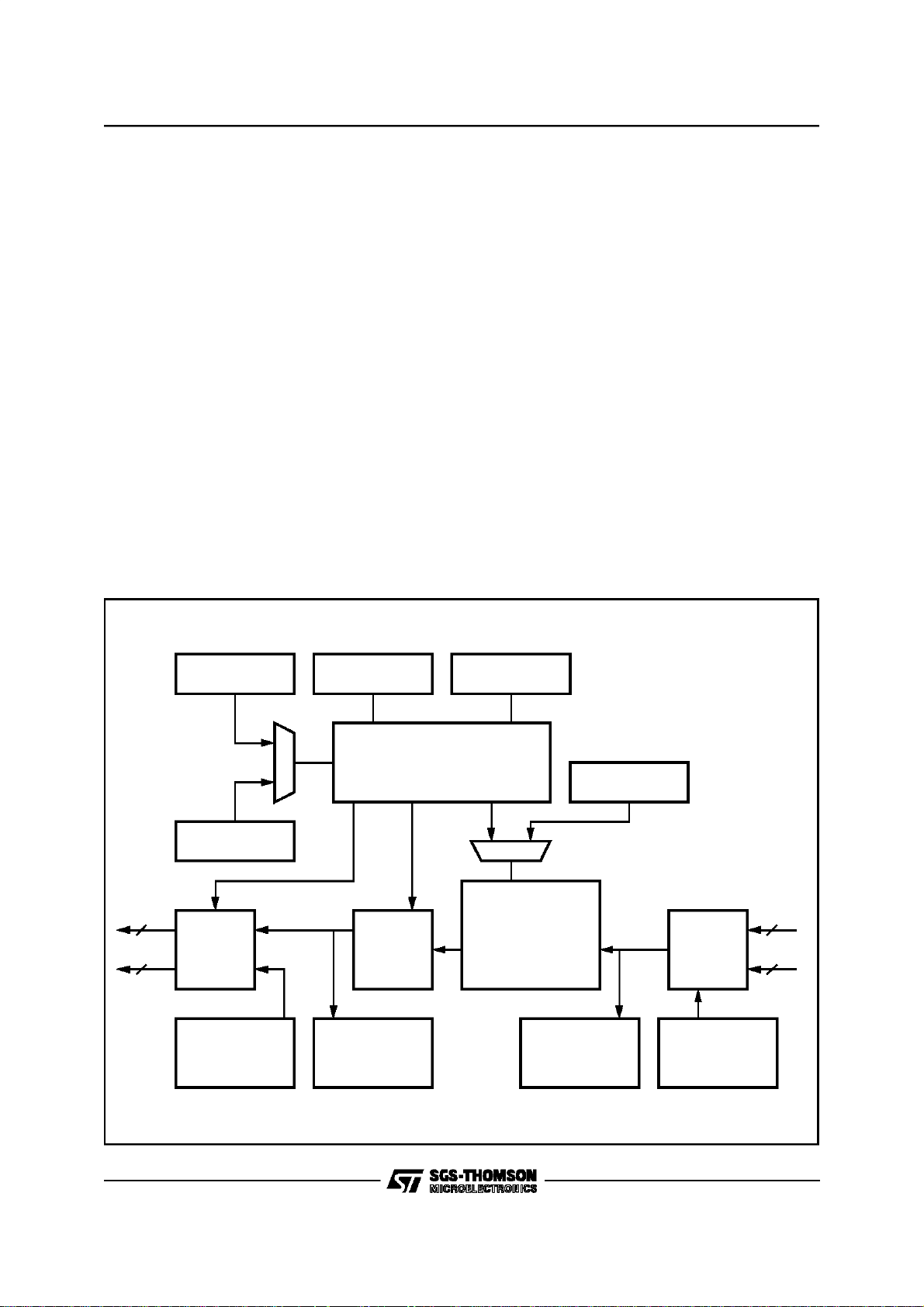
DESCRIPTION
The Line Card Interface Controller, STLC5460, is
a monolithic switching device for the path control
of up to 128 channels of 16, 32, 64 kbps bandwidth. Two consecutive 64 kbps channels may
also be handled as a quasi single 128 kbpschannel. For these channels, the LCIC performs nonblocking space time switching between two serial
interfaces: the system interface (or PCM interface) and the general componentinterface (GCI).
PCM interface can be programmed to operate at
different data rates between 2048 and 8192 kbps.
The PCM interface consists of up to four duplex
ports with a tristate indication signal for each output line. The GCI interface can be selected to be
PCM interfaceat 2Mbit/s.
The LCIC can be programmed to communicate
with GCI compatible devices such as STLC3040
(SLIC), STLC5411 (U interface) and others. The
device manages the layer 1 protocol buffering the
Command/Indicateand Monitor channels for GCI
compatible devices.
Due to its capability to switch channelsof different
BLOCK DIAGRAM
bandwidths, the STLC5460 can handle up to 16
ISDN subscribers with their 2B+D channel structure in GCI configuration,or up to 16 analog subscribers.Since its interfacescan operate at different data rates, the LCIC is an ideal device for
data rate adaptationbetween PCM interface up to
8Mb/sand GCI at 2Mb/s.
The device gives the possibility of checking the
correct communication inside the PBX or Public
CentralOffice providing:
- independentPCM delay setting
- PCM comparisonfunction
-Pseud oRando mSequenc eGener atorandAnalyse r.
Moreover, the LCIC is one of the key building
blocks for networks with either central, distributed
or mixed signaling and packet data handling architectures associated with ST5451 (HDLC controller).
The device iscontrolled by a standard8 bit parallel microprocessor interface with a multiplexed
address-data bus. The device may optionally be
controlledby separateaddress and data buses.
4 PCM
2 GCI
DESTINATION REG COMMAND REG SOURCE REGISTER
(ADDRESS) (DATA) (DATA)
COMMAND MEMORY
194 WORDS OF 14 BITS
6 bits
COUNTERS
1 bit for 16 tristate
PARALLEL
SERIAL
SHIFTING
C/I, MON
TRANSMIT
16
INDIPENDENT
CONTROLLERS
SPECIAL
SWITCH
16, 32, 64
KB/S
EXTRACTION
2x64
Kbit
CHANNEL
AT
SWITCHING
MEMORY
194
BYTES
(4PCM+2GCI + 2
CHANNEL -INSERTION- =
128+64+2=194)
RECEIVER
D94TL160A
C/I, MON
COUNTERS
SERIAL
PARALLEL
SHIFTING
INSERTION
2x64
Kbit
CHANNEL
4 PCM
2 GCI
2/54
Page 3

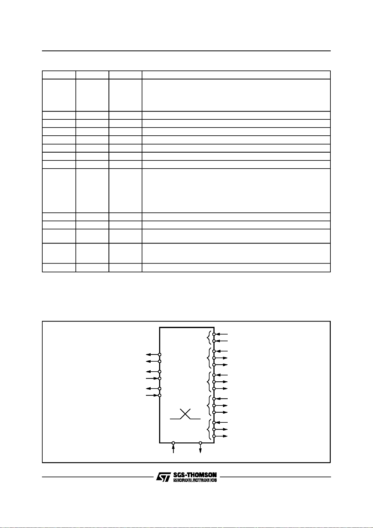
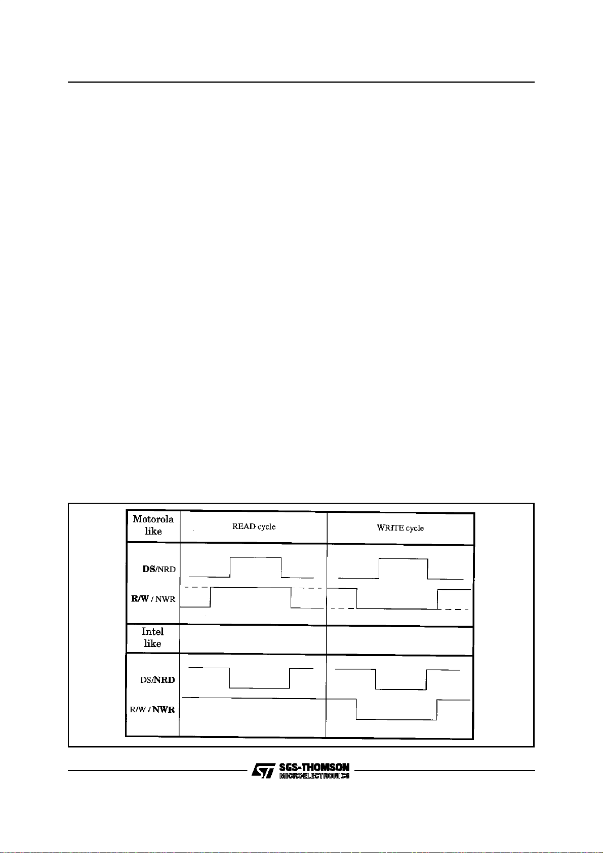
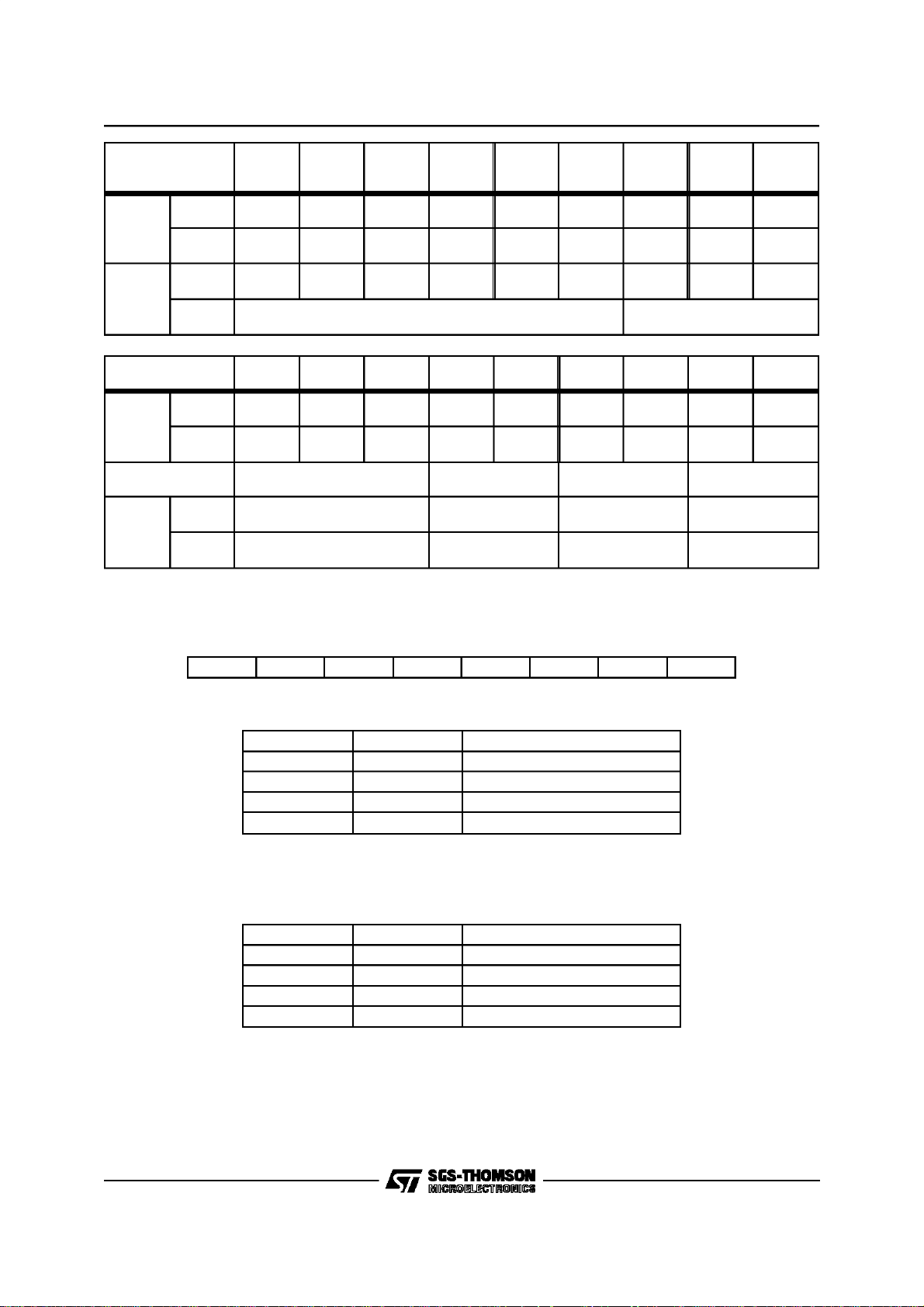
PIN DEFINITIONSAND FUNCTIONS
Symbol Pin number Type(*) Function
VDD1 1 I Supply Voltage 5V,±5% .
A0 2 I (**) Non Multiplexed Mode:
RxD3
RxD2
RxD1
RxD0
3
4
5
6
I Receive PCM interface Data : Serial data is received at these lines at
A1 7 I (**) Non Multiplexed Mode:
TSC0
TSC1
TSC2
TSC3
TxD0
TxD1
TxD2
TxD3
8
10
12
14
9
11
13
15
OD Tristate control for the PCM interface. These lines arelow when the
O Transmit PCM interface Data : Serial data issent by theselines at standard
PFS 16 I PCM interface framesynchronization pulse.
PDC 17 I PCM interface data clock, singleor double rate.
A2 18 I (**) Non Multiplexed Mode:
AD0
AD1
AD2
AD3
AD4
AD5
AD6
AD7
19
20
21
22
23
24
25
26
I/O Address Data Bus. Ifthe multiplexed address/data µP interface bus mode is
VSS1 27 I Ground : 0V
DS/NRD 28 I Motorola like mode: Data Strobe
RW/NWR 29 I Motorola like mode: Read/Write
NCS 30 I Not Chip select. A low on this line selects the STLC5460 for a read/write
this input interfaces to the system’s address bus to select aninternal
register for a read or write access.
Multiplexed Mode:
A0 at VDD, NRDY/NWAIT pin delivers NWAIT
A0 at VSS, NRDY/NWAIT pin delivers NREADY
standard TTL orCMOS levels.
this input interfaces to the system’s address bus to select aninternal
register for a read or write access.
Multiplexed Mode:
A1 at VDD, NCS signal provided by the system is not inverted by the circuit.
A1 at VSS, NCS signal provided by the system is inverted by the circuit.
corresponding TxD outputs are valid.
TTL or CMOS levels. These pins can be tristated.
this input interfaces to the system’s address bus to select anintenal register
for a reador write access.
Multiplexed Mode:
A2at VDD, AS/ALE signal providedby the system is notinvertedby the circuit
A2 at VSS, AS/ALE signal providedby the system isinverted by the circuit
selected these pins transfer data and commands between theµP and the
STLC5460.
If a demultiplexed mode is used, these bits interface with the system data
bus.
Intel Like Mode: Not Read
The signal indicates aread operation, active low
Intel Like Mode: Not Write
The signal indicates aWrite operation, active low.
operation.
STLC5460
(*): (I)Input
(O) Output
(IO) In/Output
(OD) Open Drain
(**): With Pull up resistance.
3/54
Page 4
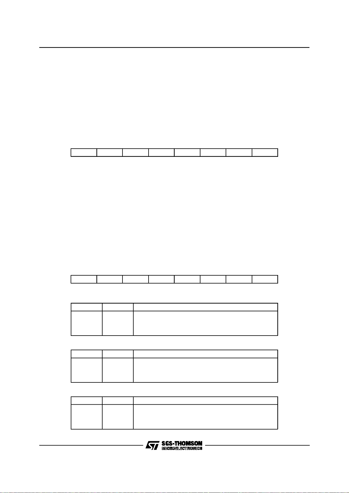
STLC5460
PIN DEFINITIONSAND FUNCTIONS (continued)
Symbol Pin n PLCC Type Function
AS/ALE 31 I Multiplexed A/D mode:
INT 32 OD Interruptline, active low.
DCL 33 0 Data clock output.
FSC 34 O Frame synchronization output.
VDD2 35 I Power supply : 5V
VSS2 36 I Ground.
DIN1 37 I GCI Data input 1
DIN0 38 I GCI Data input 0
A3 39 I (**) Non Multiplexed Mode:
DOUT0 40 O GCI Data Output 0
DOUT1 41 O GCI Data Output 1
PO 42 I(**) P0 at VSS: variable access mode
NRDY/N
43 OD If P0 at VSS:
WAIT
RES 44 I Reset. A logical high onthis input forces theSTLC5460 into the reset state
(*): (I)Input
(O) Output
(IO) In/Output
(OD) Open Drain
(**): With Pull up resistance.
used to latch the address from ADn
Non Multiplexed A/D Mode:
This pin at VSS indicates Intel like interfaces
This pin at VDD indicates Motorola like interfaces.
this input interfaces to the system’s address bus to select aninternal
register for a read or write access.
Multiplexed Mode:
A3 at VDD, DS/NRD signal provided by the system is not inverted by the
circuit
A3 at VSS, DS/NRD signal provided by the system isinverted by the circuit
P0 at VDD: fixed access mode
Intel like mode: this pin delivers NRDY
Motorola mode: this pin delivers NWAIT
Figure 1:
4/54
GCI and PCM Interfaces.
DCL
FSC
DOUT0
DIN0
DOUT1
DIN1
CLOCKS
PCM0
MUX0/GCI0
PCM1
MUX1/GCI1
PCM2
PCM3
LCIC
MICROPROCESSOR INTERFACE
PDC
PFS
RxD0
TxD0
TSC0
RxD1
TxD1
TSC1
RxD2
TxD2
TSC2
RxD3
TxD3
TSC3
D94TL159A
Page 5

STLC5460
LINE CARD APPLICATIONS
The LCIC is designed to fit both digital and analogue line cardarchitectures.
It supportsup to 16 ISDN subscribers or 16 voice
subscribers.The level 1 devicesare connectedto
ST5451 circuits to perform the D channel handling.
The clock frequency of PDC is equal to once or
twice the datarate, See fig 1 and 2. Whenoperating at single rate (2048 kb/s) and not at double
clock frequency (4096 kHz), an onchip clock frequency doubler providesa 4098 kHz clock for the
GCI interface (DCL).
The rising edge of PFS signal is used to determine the first bit of the first time slot of the frame.
The length of PFS pulse is one bit-time at least
Analogue Line Card
In analogue line cards LCIC controls signalling,
voice and datapath of 64 kb/s channels.
When used in combinationwith L3040/L3000N,it
allows to implement an optimised line card architecture:
the LCIC controls the configuration of L3040 and
exchange signalling with the L3040.
and the length between two pulses can be also
one bit time.
After reset,the LCICreaches synchronismhaving
received two consecutive correct PFS pulses.
Synchronisationis consideredlost by the device if
the PFS signal is not repeated with the correct
repetition rate which has been stored by the circuit at the beginningof synchronisation research.
The LSYNC bit in the Interrupt Register indicates
if the component is synchronised or not: a logical
Digital Line Card
In digital line cards LCIC controls the configuration of Level 1 circuits (U or S Interface) by
means of MON channel configuration and performs activation/deactivation by means of Command/Indicate protocol. LCIC switches the B
channels and can switch the D channels if the
processingis centralised.
0 indicates the synchronous state, a logical ”1”
showsthat the synchronismhas been lost.
The relation between the framing signal PFS and
the bit stream is controlled by the contents of
IPOF, OPOF and CPOF registers. These registers denote the number of bit times the PCM
frame is shifted. EachPCM multiplex can be programmed withdifferentshifts .
Without programming the bit shift function of the
FUNCTIONAL DESCRIPTION
PCM INTERFACE
PCM interface, the rising edge of the PFS signal
marks the first bit of input PCM frame and the
first bitof output PCM frame.See Fig 3
The PCM Interface Registers configure the data
transmitted or received at the PCM port, for one
PCM, the maximum data rate can change depending on the Mode selected:
PCM Mode 0: maxrate 2048kb/s with fourPCM
portsactive
PCM Mode 1: maxrate 4096 kb/s with two PCM
portsactive
PCM Mode 2: maxrate 8192 kb/s with one PCM
portsactive.
The ”actual data” rate may be varied in a wide
range without programming.
An automate computes the number of clock per
frame. Hence, the data rate can be stepped in 8,
16 or 32 kb/s in increments in PCM mode 0, 1, 2
GCI Interface
The Monitor and the Command/Indicatechannels
may be validated or not, in this second case the
B3 and B4 channels become standard channels
at 64 kb/s.
When validatedCommand/Indicatechannel may
be configured with fourbits for digital cards or six
bits for analogue cards.
The clocks (Bit clock and frame clock) are delivered by the device with double rate clocking or
simple rate clocking.
FSC and DCL are output signals derived from
PFSand PDC which are inputsignals.
respectively.
GCI PCM
DCL clock kHz
Simple (*) Double Simple Double
2.048 4.096 2.048 2.048 2.048 Mode 0
2.048 4.096 2.048 4.096 2.048 Mode 0
2.048 4.096 2.048 4.096 4.096 Mode 1
2.048 4.096 2.048 8.192 4.096 Mode 1
2.048 4.096 2.048 8.192 8.192 Mode 2
2.048 4.096 2.048 16.384 8.192 Mode 2
(*) as GCI formatbut with simple clock.
Data kb/s
PDC Clock (kHz)
Data rate kb/s Mode
5/54
Page 6
STLC5460
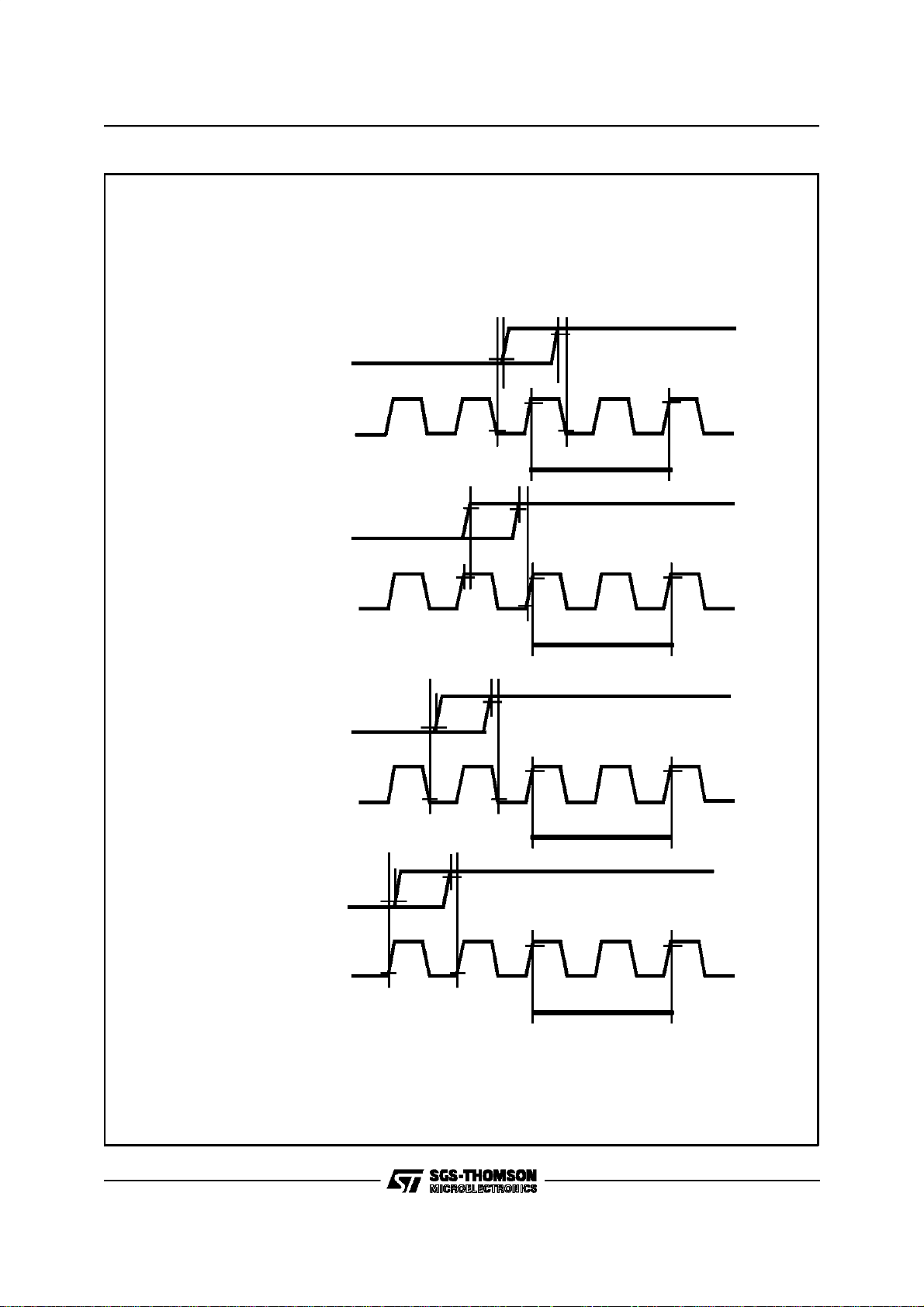
Figure 1: PCMInterface. Alignmentin doubleclock mode.
Clocks received by the circuit
Mode not delayed:
PFS
DCL=1
DEL=0
PFSP=0
PDC
PFS
First bit of the frame
DCL=1
DEL=0
PFSP=1
Mode delayed:
DCL=1
DEL=1
PFSP=0
DCL=1
DEL=1
PFSP=1
PDC
First bit of the frame
PFS
PDC
First bit of the frame
PFS
PDC
First bit of the frame
6/54
Page 7
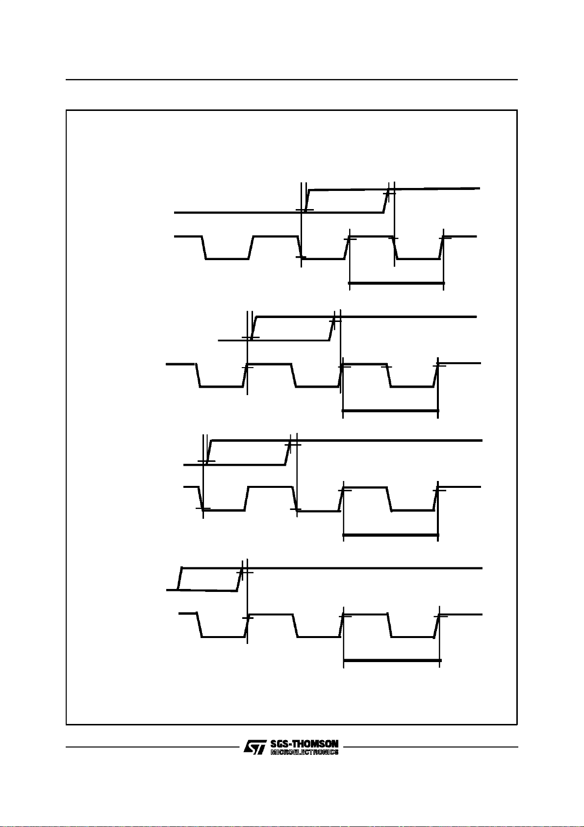
Figure 2: PCMInterface. Alignmentin simpleclock mode.
Clocks received by the circuit
PFS
PDC
STLC5460
DCL=0
DEL=0
PFSP=0
PFS
DCL=1
DEL=0
PFSP=1
PDC
Mode not delayed
PFS
DCL=1
DEL=1
PFSP=0
PDC
First bit of the frame
First bit of the frame
First bit of the frame
PFS
DCL=1
DEL=1
PFSP=1
Mode delayed
PDC
First bit of the frame
7/54
Page 8
STLC5460
Figure 3: PCMInterface. Clockand Data in/Data out.
PDC
ODL=0
GCI like
ODL=1
ISPP=0
ISPP=1
GCI like
DOUT
DOUT
DIN
DIN
Double clock DCP =1
PDC
ODL=0
DOUT
8/54
ODL=1
DOUT
DIN
Simple clock DCP=0
Page 9
STLC5460
MEMORY STRUCTURE AND SWITCHING
The LCIC contains three memories: Auxiliary
Memory (AM), Data Memory (DM) and Control
Memory (CM).
The Auxiliary Memory consists of one block divided in four parts of 16 words.
This Auxiliary Memory is used for validated data
from Monitor and Command/IndicateRx channels
and to transmit data to Monitor and Command/IndicateTx channels.
The Data Memory buffers the data input from the
PCM and the GCI interface. It has a capacity of
128 + 64 time slots to buffer 4 PCM frame of 32
time slots and two GCI interfaces. It is written periodically onceevery 125 microseconds controlled
by theinput countersassociated to PCM interface
and to GCI interface.To perform the switching the
loopback function, this memory is read, random,
in accordancewith the controlmemory
The Control Memory has a capacity of 128 + 64
words of 14 bits: 8 of data and6 ofcode. The 14
bits are written random, via microprocessor interface and read cyclically under the control of
the output counters associated to PCM interface
and GCI interface.
For control memory access and different functions, threeregisters are provided:
destinationregister:
it contains the address of a specific location of
the controlmemory;
source register :
it contains the data (to be written or read) of the
control memory corrisponding to the address indicatedby thedestination register;
commandregister:
it contains the code (6 bits to be written or read)
of the control memory.
The content of command register defines the different capabilities: switching at 64 kb/s, 32 kb/s,
16 kb/s, loopback and also extraction/insertion
from themicroprocessorinterface.
A memory access using the actual command register and source registeris performedupon every
destination register write access. The processing
of the memory access takes at most 488ns.
MICROPROCESSORINTERFACE
After Reset, the Microprocessor interface is in
non-multiplexed mode (Address bus and Data
bus mustbe non-multiplexed):
if ALE pin is hardwired at VSS, the Microprocessor interface is Motorola like, Address/Data are
non-multiplexed.
if ALE pin is hardwired at VDD the Microprocessor interface is Intel like, Address/Data are nonmultiplexed.
After Reset,as soon as two successiveedges are
detected on ALE pin (Rising and falling edges)by
the circuit the Microprocessor interface switches
in multiplexed mode (Address bus and Data bus
must be multiplexed). The circuit is set automaticallyin Motorolalike or inIntel like mode.
For the circuit Address bus and Data bus multiplexed or not multiplexed, the difference between
Motorolalikeand Intellikemodeisshowedin fig. 4.
Figure 4.
9/54
Page 10
STLC5460
The microprocessor interface type is set via P0
pin as shown hereafter :
P1 is an outputandit isnot used if P0 = 1.
The device selects automatically either Motorola
interfaceor IntelInterface.
P0 P1 Automatical selection
1 Z Intel MUX mode
Motorola MUX mode
Intel DEMUX mode
Motorola DEMUX mode
0 If A0 = 1 P1 pin delivers WAIT automatically
If A0 = 0 P1 pin delivers READY automatically
Moreover, for a multiplexed mode µP interface,
A1 to A3 pinsmean :
A1 = 1: CS signalprovided by the systemis not
inverted by the device
A1 = 0: CS signal provided by the system is inverted by the device
A2 = 1: AS signal provided by the system is not
inverted by the device
A2 = 0: AS signal provided by the system is inverted by the device
A3 = 1: DS signal provided by the system is not
inverted by the device
A3 = 0: DS signal provided by the system is inverted by the device.
C/I AND MON CHANNELS, EXTRA CHANNELS
The Command/indicateand Monitor channelscan
be validatedor not:
if validated, the C/I and MON protocol controllers
operate and it is not possible to use this channels
for switching, if not validated the protocols are inhibited and the channels can be used as extrachannels for switching.
Command/IndicateProtocol
Sixteen C/I channelsare implemented,one bit of
the configuration register MCONF1, indicates the
number of bits of the primitive (four or six bits) for
all the channels.
To transmit a primitive into one of the 16 channels, the mp loads the primitive (4 or 6 bits) into
source register and the number of the C/I channel into destination register with W/R bit of command registerat ”0”.
The two more significant bits of the source register indicates if the primitive, bit0/5 of the same
register, has not been transmittedyet, transmitted
once, twice or more .
When a new primitive has been received twice
identical, on one of the 16 C/Ichannels, an interrupt is generated,the number of the C/I channel
(4 bits) is written in the Receive C/I status register , and the primitive received is in the Auxiliary
Memory,all accessibleto theµp
Moreover, the microprocessor can read directly
the 16 primitives that have been received and
stored into the Receive C/I Memory. To read this
memory the µp load in the Source Register the
number of Receive C/I channel it wants, and in
the destinationregister reads the primitive (4 or 6
bits) with a seventh bit which indicates whether
the primitive has been received once or twice
identical. vedi figura read aux mem Receive C/I
channels.
Monitor Channel Protocol
Sixteen Monitor channels are implemented. To
transmit a message the µp load into destination
register with W/R bit of Command Register at 1
the number of MON channels, and into source
register the message; this byte is transmitted if
BYTE Bitof Command Register is at 1.
This procedure is repeated for each byte of the
message if it islonger than onebyte.
When a new byte has been received twice identical from oneof the sixteen Monitor channels
an interrupt is generated, the number of MON
channel (4 bits) is written in Receive Monitor
StatusRegister and the last byte received is written in Receive data Monitor Channel Memory.
The remote transmitter will transmit the next byte
after reading of this register by the local microprocessor.
INSERTION- EXTRACTION
This function allows to insert data into GCI and
PCM channels and to extract data from GCI and
PCM interface. These data are provided either by
the microprocessor or by an internal Pseudo Random SequenceGenerator.
Insertion
Two programmable registers (Insert A and B)
contain the data to insert into two output time
slots continuously. To perform an insertion, four
registersare programmedby the microprocessor:
- in the Insert A and/or B Registersit writes the
data to insert.
- in the Source registers it writesthe A and/or B
registeraddress
- in the DestinationRegister it writes the output
interface, PCM or GCI, and the Time Slot selected.
10/54
Page 11

STLC5460
- in the Command Register it writes the indication if insert into 64 kb/s, 32 kb/s or 16 kb/s
channel.
When the data has been inserted, status bit
(INS) of status register is put at logical 1 and an
interrupt is generated.
Extraction
Two programmable registers (Extract A and B)
contain the data extracted from two input time
slots. To perform an extraction, three registers
LIST OF REGISTER
Name MUX Mode
AD5 to AD1 (H) RBS A3 to A0 RBS
IIR
COMP
MCONF1
MCONF2
PCONF
CPOF
IPOF
OPOF
IPSH1
IPSH2
OPSH1
OPSH2
IPASS
OPASS
IMASS
OMASS
00000
00001
00010
00011
00100
00101
00110
00111
01000
01001
01010
01011
01100
01101
01110
01111
(00)
(01)
(02)
(03)
(04)
(05)
(06)
(07)
(08)
(09)
(0A)
(0B)
(0C)
(0D)
(0E)
(0F)
are processed by the microprocessor:
- Extract A and/or B Registers to read the data
extracted.
- The Sourceregister to indicate the input interface, PCM or GCI, and the Time Slot selected.
When the data is loaded in Extract A or Extract B Register, the bit EXT of STATUS register is put at logical1,and an interrupt is generated.
Read
Only
X
X
X
X
X
X
X
X
X
X
X
X
X
X
X
X
DEMUX Mode
0000
0001
0010
0011
0100
0101
0110
0111
1000
1001
1010
1011
1100
1101
1110
1111
X
0
0
0
0
0
0
0
0
0
0
0
0
0
0
0
STATUS
ECR
CMR
SRC
DST
INSA
INSB
EXTA
EXTB
INT
MASK
RMOS
TMOS
RCIS
TEST
10001
10010
10011
10100
10101
10110
10111
11000
11001
11010
11011
11100
11101
11110
11111
(11)
(12)
(13)
(14)
(15)
(16)
(17)
(18)
(19)
(1A)
(1B)
(1C)
(1D)
(1E)
(1F)
X
X
X
X
X
X
X
X
X
X
X
X
X
X
X
NB in Mux Mode AD7, AD6, AD0 andRDS bits are ignored
R
R
R
R
R
R
R
0001
0010
0011
0100
0101
0110
0111
1000
1001
1010
1011
1100
1101
1110
1111
1
1
1
1
1
1
1
1
1
1
1
1
1
1
1
11/54
Page 12

STLC5460
CONFIGURATION REGISTER DESCRIPTION
Initialisationand IdentificationRegister(IIR)
7 0
RBS RST T1 T0 V3 V2 V1 V0
After Reset 3F (H)
T1/T0 Testfunctions
T1 T0 Description
0 0 Normal State
0 1 Command Memory orAuxiliary Auto Reset.
1 1 Auto Test. This function is reserved for manufacturer.
1 1 Reserved. Initialise CM so that the content of each input Time Slot t of input multiplexm is
If CM = 1 (Bitof Command Register):
the six lower bits of command Register andthe eight bits of Source Register are stored
into each address of command Memory.
If CM = 0 (Bit of Command Register) :
the eight bits of Source Register are stored into each address of Monitor Auxililary
Memory and the six lower bits of SourceRegister are stored intoCommand/Indicate
Auxilliary Memory.
The 16 C/I and Monitor channels are ready to transmit and toreceive data.After
AutoReset, BUSY and T0 goes to ”0”.
- The Pseudo Random Sequence generator is connectedinstead of Insert A Register and
PseudoRandom Sequence Analyzer is connected instead of Extract A Register.
- The Command Memory is loaded thanks to a specialalgorithm in order to switch the
sequence provided by the generator into TSO of PCMO, then the contents of TSO of
PCMO into TS1 of PCMO, then the contents of TS1 of PCMO into TS2 of PCMO and
so on.
Finally, the contentsof TS31 of MUX1 are taken into account by the Pseudo Random
Sequence Analyzer.After loading Command Memory, 193 switching are setup in real
time.The analyzer receivesthe Pseudo Random Sequence from the generator after
switching.
If LP = 1, the loopback is internal.
If LP = 0, an external loopback must be performed. So, Command Memoryand Data
Memory can be checked in the same time.
switched to output Time Slot t of output multiplex m
RBS Register BankSelection.
RBS = 0. The 16 first main registersare selected(0 to 15).
RST Reset Soft.
the programmableregistersare reset.
V3/V0 these bits are fixed at 0
COMPARISONREGISTER (COMP)
7 0
NEWE TIM CP6 CP5 CP4 CP3 CP2 CP1
After Reset 00(H)
NEWE New EXTRACT.
When NEWE = 1, EXT interrupt is generated only if a new word is loaded into
EXTRACT Registers (A or B).
TIM Timer, associatedto INS of INTRegister and to TIMO/1of CPOFregister.
TIM = 1 TIM0/1bits of CPOFregister are taken into account
TIM = 0 an interrupt is generatedeach 125 µs.
12/54
Page 13

CP 6/1 Comparison6 to 1.
Bit streamof one PCM and bit stream of another PCM are compared at each bit time, if
there is difference,PDIF interruptis generated.
Comparison between
CP1 = 1 PCM0 and PCM1
CP2 = 1 PCM1 and PCM2
CP3 = 1 PCM2 and PCM3
CP4 = 1 PCM0 and PCM2
CP5 = 1 PCM1 and PCM3
CP6 = 1 PCM0 and PCM3
MULTIPLEXCONFIGURATION 1 REGISTER (MCONF1)
7 0
CIM MOM CI4MI CI4M0 - - GCIM1 GCIM0
After Reset 3F (H)
CIM Command/IndicateMode.
CIM = 1: the controller ignores the new received primitive if the previous has not been
read by the microprocessor.
STLC5460
CIM = 0: the controller overwrites the previous primitive without condition when it
receivesa newprimitive.
MOM Monitor channelMode
MOM = 1: if bytesare not receivedtwice identical the message is aborted.
MOM = 0: if bytes are not received twice identical the MOM controller doesn’t
acknowledgethe receivedbyte (GCI standard).
CI4M1 Command Indicate4 bitsfor Multiplex 1.
CI4M1 = 0: commandIndicate primitive has six bits.
CI4M1 = 1: commandIndicate primitive has four bits.
CI4M0 Command Indicate4 bitsfor Multiplex 0.
CI4M0 = 0: commandIndicate primitive has six bits.
CI4M0 = 1: commandindicate primitive has fourbits.
GCIM1 GCI Multiplex1.
GCIM1 = 1: themultiplex M1 is GCI,it includes eight GCI channels.
GCIM1 = 0: themultiplex M1 includes32 TimeSlots. (PCM like channel)
GCIM0 GCI Multiplex0.
GCIM0 = 1: theMultiplex M0 is GCI,it includes eight GCI channels.
GCIM0 = 0: themultiplex M0 includes32 TimeSlots. (PCM like channel)
MULTIPLEXCONFIGURATION 2 REGISTER(MCONF2)
7 0
- - M1D M0D ISPM TIMD MOD DCKM
After Reset FF (H)
M1D Multiplex1 Disable.
M1D = 1. Multiplex1 output is at high impedancecontinuously,
multiplex 1 inputis forced to ”1”,if it is GCI.
13/54
Page 14

STLC5460
M0D Multiplex0 Disable.
M0D = 1. Multiplex0 output is at high impedancecontinuously,
multiplex 0 inputis forced to ”1”,if it is GCI.
TIMD Timer Monitor Channel Disabled.
TIMD = 1. The timer1ms is disabledfor each TransmitMonitor Channel.
ISPM Input Sampling Multiplex.
ISPM = 0. The inputbit is sampled at half bit time.
ISPM = 1. The inputbit is sampled at 3/4 bittime.
MOD Multiplex OpenDrain.
MOD = 1. The twomultiplex outputs are open drain.
MOD = 0. The twomultiplex outputs are at low impedance
DCKM Double clock for Multiplex.
DCKM = 1.DCL is twice data rate(Ex : if Data Rate = 2048 kb/s,DCL = 4096 kHz).
DCKM = 0.DCL is simple clock.
PCM CONFIGURATIONREGISTER (PCONF)
7 0
0 TSNB DEL PFSP ODL ISPP POD SCKP
After Reset 00(H)
TSNB Time Slot numbering.
TSNB defines the order of TS on the PCM when the data rate is 4 Mb/s or 8 Mb/s
related to theorder of TS on the PCM at 2 Mb/s(see table hereafter).
DEL Delayed Mode for each PCM.
DEL = 1. A delay of one clockpulse is appliedto thefirst bit of the frameof eachPCM.
DEL = 0. PFS indicates the first bit of the frame for each PCM (if OFFSET and shift are
zero).
PFSP PCM FrameSynchronisationSampling.
PFSP = 0. PFS signal is sampled on the fall edge of PDC signal.
PFSP = 1. PFS signal is sampled on the rise edge of PDCsignal.
ODL Output Delay.
ODL = 0. The bits areshifted out withzero delay.
ODL = 1. The bits areshifted out witha delay of one half bittime.
ISPP Input Sampling PCM.
ISPP = 0. The input bit is sampled at half bit time.
ISPP = 1. The input bit is sampledat 3/4 bit time.
POD PCM OpenDrain.
POD = 1. The PCM outputs are open drain
POD = 0. The PCM outputs are at lowimpedance.
SCKP Simple clock for PCM.
SCKP = 0. PDC signal is twice data rate. (Ex : if data rate = 2048 kb/s, PDC = 4096
kHz).
SCKP = 1. PDC is simple clock
14/54
Page 15
TS and PCMn
at 4 Mb/s
with n = 0 or 2
TSNB = 1
TSNB = 0
TS at
2Mb/s
PCM at
2Mb/s
TS at
2Mb/s
PCM at
2Mb/s
STLC5460
TS0 TS1 TS2 TS3 TS30 TS31 TS32 TS62 TS63
TS0 TS0 TS1 TS1 TS15 TS15 TS16 TS31 TS31
PCMn PCMn+1 PCMn PCMn+1 PCMn PCMn+1 PCMn PCMn PCMn+1
TS0 TS1 TS2 TS3 TS30 TS31 TS0 TS30 TS31
PCMn PCMn+1
TS and PCM0
at 8 Mb/s
TSNB = 1
TS and PCM
at 8Mb/s
TSNB = 0
TS at
2Mb/s
PCM at
2Mb/s
TS at
2Mb/s
PCM at
2Mb/s
TS0 TS1 TS2 TS3 TS4 TS124 TS32 TS62 TS63
TS0 TS0 TS0 TS0 TS1 TS31 TS31 TS31 TS31
PCM0 PCM1 PCM2 PCM3 PCM0 PCM0 PCM1 PCM2 PCM3
TS0 to TS31 TS32 to TS63 TS64 to TS95 TS96 to TS127
TS0 to TS31 TS0 to TS31 TS0 to TS31 TS0to TS31
PCM0 PCM1 PCM2 PCM3
COMPLEMENTARY PCM OFFSET REGISTER (CPOF)
7 0
PMD1 PMD0 TIM1 TIM0 OOF1 IOF0 IOF1 IOF0
After Reset 00(H)
PMD1/0 PCMMode
PMD1 PMD0 The PCM are at
0 0 2048 kbit/s
0 1 4096 kbit/s
1 0 8192 kbit/s
1 1 Not used.
TIM 1/0 thesebits are taken into account only if bit TIM of COMPregister is at 1; in this case an interrupt is generatedperiodicallyand TIM 1/0 definesthe period
TIM1 TIM0 Period
0 0 1ms
0 1 8ms
1 0 64ms
1 1 250ms
OOF1/0 Output Offset 1/0.
These two bitsare associated withOOF2/9 ofOPOFRegister.
IOF1/0 InputOffset 1/0.
These two bitsare associated withIOF2/9 of IPOFRegister.
15/54
Page 16

STLC5460
INPUT PCM OFFSET REGISTER (IPOF)
7 0
IOF9 IOF8 IOF7 IOF6 IOF5 IOF4 IOF3 IOF2
IOF9/2 InputPCM Offset 9 to 2.
Associated with IOF1/0, these ten bits indicate the delay between PFS signal and the
first bit of the frame,for each input
OUTPUT PCM OFFSET REGISTER (OPOF)
7 0
OOF9 OOF8 OOF7 OOF6 IOF5 OOF4 OOF3 OOF2
OOF9/2 Output PCM Offset9 to2.
Associated with OOF1/0 of complementary offset register, these ten bits indicate the
delay betweenbit 0 of theframe out going versus bit 0 of the frame incoming.
INPUT PCM SHIFT 1 (IPSH1)
7 0
0 P1SH2 P1SH1 P1SH0 0 P0SH2 P0SH1 P0SH0
After Reset 00(H)
After Reset 00(H)
After Reset 00(H)
P1SH2/0 PCM1 Shift 2 to 0.
This number (0 to 7) is added to Input PCM offset to obtainthe totalshift of the frame of
PCM1.
P0SH2/0 PCM0 shift 2 to 0.
This number (0 to 7) is added to Input PCM offset to obtainthe totalshift of the frame of
PCM0.
INPUT PCM SHIFT 2 (IPSH2)
7 0
0 P3SH2 P3SH1 P3SH0 0 P2SH2 P2SH1 P2SH0
P3SH2/0 PCM3 Shift 2 to 0.
This number (0 to 7) is added to Input PCM offset to obtainthe totalshift of the frame of
PCM3.
P2SH2/0 PCM2 Shift 2 to 0.
This number (0 to 7) is added to Input PCM offset to obtainthe totalshift of the frame of
PCM2.
OUTPUT PCM SHIFT 1 (OPSH1)
7 0
P1E P1SH2 P1SH1 P1SH0 P0E P0SH2 P0SH1 P0SH0
After Reset 00(H)
After Reset 00(H)
P1E OutputPCM1 Enable.
P1E = 0. PCM1 outputis at high impedance.
P1E = 1. PCM1 outputis enable.
16/54
Page 17
P1SH2/0 PCM1 shift 2/0.
This number (0 to 7)is addedto output PCM offsetto obtain the totalshift of the frame of
PCM1.
P0E OutputPCM2 Enable.
P0E = 0. PCM0 outputis at high impedance.
P0E = 1. PCM0 outputis enabled.
P0SH2/0 PCM0 Shift 2/0.
This number (0 to 7) is added to output PCM offset to obtain the total shiftof the frame of
PCM0.
OUTPUT PCM SHIFT 2 (OPSH2)
7 0
P3E P3SH2 P3SH1 P3SH0 P2E P2SH2 P2SH1 P2SH0
P3E OutputPCM3 Enable.
P3E = 0. PMC3 outputis at high impedance.
P3E = 1. PCM3 outputis enabled.
P3SH2/0 PCM3 Shift 2/0.
This number (0 to 7) is added to output PCM offset to obtain the total shiftof the frame of
PCM3.
STLC5460
After Reset 00(H)
P2E OutputPCM2 Enable.
P2E = 0. PCM2 outputis at high impedance.
P2E = 1. PCM2 outputis enabled.
P2SH2/0 PCM2 shift 2/0.
Thisnumber(0to7)isaddedto outputPCMoffsettoobtainthetotalshiftoftheframeof PCM2
INPUT PCM ASSIGNMENTREGISTER (IPASS)
7 0
IP31 IP30 IP21 1P20 1P11 1P10 1P01 1P00
After Reset E4(H)
IP31/IP30 Incoming PCM3 Assignment.
IP31 IP30 Incoming PCM3 receives data from
0
0
1
1
0
1
0
1
Pin RxD0
Pin RxD1
Pin RxD2
Pin RxD3 (Defaultvalue)
IP21/IP20 Incoming PCM2 Assignment.
IP21 IP20 Incoming PCM2 receives data from
0
0
1
1
0
1
0
1
Pin RxD0
Pin RxD1
Pin RxD2 (Defaultvalue)
Pin RxD3
IP11/IP10 Incoming PCM1 Assignment.
IP11 IP10 Incoming PCM1 receives data from
0
0
1
1
0
1
0
1
Pin RxD0
Pin RxD1(Defaultvalue)
Pin RxD2
Pin RxD3
17/54
Page 18

STLC5460
IP01/IP00 Incoming PCM0 Assignment.
IP01 IP00 Incoming PCM2 receives data from
0
0
1
1
OUTPUT PIN ASSIGNMENT REGISTER(OPASS)
7 0
OP31 OP30 OP21 OP20 OP11 OP10 OP01 OP00
OP31/OP30 OutputPin 3 Assignment.
OP31 OP30 Pin TxD3 receives data from
0
0
1
1
OP21/OP20 OutputPin 2 Assignment.
OP31 OP30 Pin TxD2 receives data from
0
0
1
1
0
1
0
1
0
1
0
1
0
1
0
1
Pin RxD0(Defaultvalue)
Pin RxD1
Pin RxD2
Pin RxD3
After Reset E4(H)
Outgoing PCM0
Outgoing PCM1
Outgoing PCM2
Outgoing PCM3 (Default Value)
Outgoing PCM0
Outgoing PCM1
Outgoing PCM2 (Default Value)
Outgoing PCM3
OP11/OP10 OutputPin 1 Assignment.
OP11 OP10 Pin TxD1 receives data from
0
0
1
1
0
1
0
1
Outgoing PCM0
Outgoing PCM1 (Default Value)
Outgoing PCM2
Outgoing PCM3
OP01/OP00 OutputPin 0 Assignment.
OP01 OP00 Pin TxD0 receives data from
0
0
1
1
0
1
0
1
Outgoing PCM0 (Default Value)
Outgoing PCM1
Outgoing PCM2
Outgoing PCM3
INPUT MULTIPLEX ASSIGNMENTREGISTER (IMASS)
7 0
- - - - 0IM10IM0
After Reset 04(H)
IM1 IncomingMultiplex 1 Assignment.
IM1 Incoming Multiplex 1 receives data from
0
1
Pin DIN0
Pin DIN1 (DefaultValue)
18/54
Page 19

IM0 IncomingMultiplex 0 Assignment.
IM0 Incoming Multiplex 0 receives data from
0
1
Pin DIN0 (DefaultValue)
Pin DIN1
OUTPUT MULTIPLEX ASSIGNMENT REGISTER (OMASS)
7 0
- - - - 0 DO1 0 DO0
After Reset 04(H)
DO1 Output1 Pin Assignment.
DO1 DOUT 1 pin receives datafrom
0
1
OutgoingMultiplex 0
OutgoingMultiplex 1 (Defaultvalue)
DO0 Output0 Pin Assignment.
DO1 DOUT 0 pin receives datafrom
0
1
OutgoingMultiplex 0 (Defaultvalue)
OutgoingMultiplex 1
STLC5460
WORKINGREGISTERDESCRIPTION
Command Register (CMR)
7 0
R/W CM CR5 CR4 CR3 CR2 CR1 CR0
After Reset 00(H)
R/W Read/Write
R/W = 0. Writememory.
Address bits are provided by the Destination Register (DST)
Data bits are provided by the SourceRegister (SRC)
R/W = 1. Read Memory.
Address bits are provided by the Destination Register (DST)
Data bits willbe inSource Register(SRC) when BUSY (Status Register) will go to ”0”.
CM Commandmemory.
CM = 1 Access to CommandMemory
CM = 0 Access to Auxiliary Memory.
CR 5/0 The meaning of these bits depends on the value of CM and R/W. The description is
given thereafter.
CM = 1
Command Memory
CM = 0
Auxiliary Memory
CommandRegister Bit 5 to 0 Subchannelconfiguration Commandif Write Memory
Statusif Read Memory
SourceRegister 1 of 192 Input Time Slots or 1 of
2 InsertionRegisters
DestinationRegister 1 of 192 OutputTime Slots or 1
of 2 ExtractionRegisters
Byteif MONchannel or Primitive
if C/I channel.
1 of 16 MONchannels
or 1 of 16 C/I channels
Followingyou will find a detailed explanationcase by case of the meaningof all the bits of this register.
19/54
Page 20

STLC5460
FIRST CASECM = 1: ACCESS TO COMMAND MEMORY
CM CR5 CR4 CR3 CR2 CR1 CR0
R/W 1 CH1 CH0 SS1 SS0 DS1 DS0
After Reset 00(H)
R/W Read/Write
R/W = 0 (Write). The eight bits of Source Register and the six lower bits of this
Command Register are loaded into the Command Memory (14 bits). The Address bits
are given by the Destination Register (8 bits). Write cycle starts when Destination
Register is loaded by the microprocessor.
R/W = 1 (Read).
The 14 bits of Command memory addressed by the Destination Register are loaded
respectively into Command Register (6 bits) and Source Register (8 bits). Read cycle
starts whenDestination Register is loaded by the micro-processor.
CH0/1 Channel Data Rate
CH1 CH0 Description
00
0116kb/ssubchannel is selected
1032kb/ssubchannel is selected
1164kb/schannel is selected
During the time slot selected, the output is at high impedancefor the subchannelsnot selected.
The output is at high impedance during the time slot selected
SS 0/1 SourceSubchannel selected.
Data Rate SS1 SS0 Source channel
16kb/s
32kb/s 0 0 Bits 4 to 5
0 0 Bits 6-7
0 1 Bits 4-5
1 0 Bits 2-3
1 1 Bits 0-1
0 1 Bits 0 to 3
Bit 7 is trasmittedfirst.
DS 0/1 DestinationSubchannelselected.
Data Rate SS1 SS0 Source channel
16kb/s
32kb/s 0 0 Bits 4 to 5
0 0 Bits 6-7
0 1 Bits 4-5
1 0 Bits 2-3
1 1 Bits 0-1
0 1 Bits 0 to 3
Bit 7 is trasmittedfirst.
20/54
Page 21

STLC5460
SECONDCASE CM = 0: ACCESSTO AUXILIARYMEMORY
Microprocessor writes Auxiliary Memory to transmit Primitives for each TX C/I channel and to transmit
Bytes of message for eachTX MONchannel.
Microprocessorreads Auxiliary memory to recover Primitive receivedby each RX C/I channel and to re-
cover the message received byeach RX MON channel.
TX CommandIndicate channel - Selectedby Destination Register (DST)
CM CR5 CR4 CR3 CR2 CR1 CR0
R/W 0 - - - - PT1 PT0
R/W = 1 Read auxiliarymemory
After writing thisregister with R/W=1 and when BUSY(statusregister)has gone to 0, the
bits of the registerhave the followingmeaning:
CR5/CR2 Not used
PT0/1 Primitive trasmitted
PT1 PT0 Status
00
01Primitive hasbeen transmittedonce
10Primitive hasbeen transmittedtwice
11Primitive hasbeen transmittedmore than twice.
Primitive hasnot been transmittedyet
R/W = 0 Write auxiliarymemory.
CR0/CR5 not used
RX Command Indicate channel - Selected by Destination Register (DST)
CM CR5 CR4 CR3 CR2 CR1 CR0
R/W 0 - - - - OVR PR
R/W = 1 Read auxiliarymemory
After writing this register with R/W=1 and when BUSY(status register) has gone to 0, the bits of the
registerhave thefollowing meaning:
CR5/CR2 Not used
OVR Overrun
OVR = 1. The previous primitive has not been readby themicroprocessor.
PR Primitive Received.
PR = 1. The primitive has been receivedonce
PR = 0. The primitive has been receivedtwice or more.
The primitive is in Source Register.
R/W = 0 Writing auxiliary memory.
CR0/CR5 not used
21/54
Page 22

STLC5460
TX Monitor Channel selectedby DestinationRegister.
R/W CM CR5 CR4 CR3 CR2 CR1 CR0
0 0 - - - LAST BYTE INIT
IR/W = 0 Writing auxiliarymemory.
CR5/CR3 not used
LAST Last Byte.
This bit is associatedwith BYTE.
If LAST = 1, last byte of the message.
If LAST = 0, current byte
BYTE Byte to transmit.
INIT When this bit is at 1, the MON channel defined in SRC Register is initialised and the
Monitor Channelis idle (All ”1”sare transmitted)
R/W CM CR5 CR4 CR3 CR2 CR1 CR0
1 0 - T0 ABT LAST BYTE IDLE
R/W = 1 Read auxiliarymemory
After writing this register with R/W=1 and when BUSY(status register) has gone to 0, the bits of the
registerhave thefollowing meaning:
TO Time Out = one millisecond.
This bit goes to 1 when the remote receiver has not acknowledged the byte after 1
millisecond.
ABT Abort.
ABT = 1 The remotereceiver has aborted the messagetransmitting.
LAST Last Byte.
This bit is associatedwith BYTE.
If LAST = 1, last byte of the message.
If LAST = 0, current byte.
BYTE BYTE = 1 Byte transmitting.
BYTE = 0 Byte transmittedand acknowledgedby the Remote
Receiver,a new byte can be transmitted.
IDLE IDLE = 1 Monitorchannel, A bit, E bitare at ”1”.
RX Monitor channel- Selectedby DestinationRegister
CM CR5 CR4 CR3 CR2 CR1 CR0
R/W 0 - - - AB BYTE EOM
R/W = 1 Read auxiliarymemory
After writing this register with R/W=1 and when BUSY(status register) has gone to 0, the bits of the
registerhave thefollowing meaning:
AB Abort.
AB = 1 The receiverhas detectedan error during the transmission.
22/54
Page 23

STLC5460
BYTE New byte.
Byte = 1 A new byteis availablein theSourceRegister
EOM End of Message
EOM = 1 : there is no significant byte in the Source Register. The previous byte which
had been receivedwas the last.
R/W = 0 Write auxiliarymemory.
Writing initiatesthe RX MonitorChannel.
CR0/CR5 not used
SOURCEREGISTER (SRC)
When the bit CM of commandregister is at one, thisregister contains the data to be writtenin the control
memory at the address indicated by the destination Register. It rappresents the address of the data
memory,or ofone ofthe insert register,correspondingto the input data to be switched to the output indicated by the destinationregister.
Followingyou will find a detailed explanationcase by case of the meaningof all the bits of this register.
First case CM= 1 (Bitof Command Register)
CommandMemory is selected.
7 0
PCM SR6 SR5 SR4 SR3 SR2 SR1 SR0
After Reset 00(H)
PCM = 1 The source is PCMInput.
PCM = 0 The source is not PCM.The Sourceis eitherMultiplexInputs (GCI) or Insert Registers.
PCM = 1
PCM SR6 SR5 SR4 SR3 SR2 SR1 SR0
1 N1 N0 TS4 TS3 TS2 TS1 TS0
After Reset 00(H)
If PCM is at 2 Mb/s
N0/1 PCMNumber : 0 to 3
TS0/4 Time Slot Number : 0 to 31
If PCM is at 4 Mb/s
N1 PCM at 4 Mb/s : 0 or 1
TS0/4 and N0 Timeslot Number : 0 to 63
N0 = TS5
If PCM is at 8 Mb/s
TS0/4 and N0/1 Time Slot Number: 0to 127.
N0 = TS5, N1 = TS6.
PCM = 0 The Source is Multiplex Input or Insertion Register.
If N1 = 0 Multiplexesare selected(GCI or not) then
N0 = 0 Multiplex number: 0
23/54
Page 24

STLC5460
N0 = 1 Multiplexnumber : 1
TS0/4 Time Slot Number: 0 to 31
If N1 = 1 Insertion Registersare selected.
N0 = 0 and TS0/4= 0. A InsertionRegister40 (H) is the source
N0 = 1 and TS0/4= 1. B InsertionRegister41(H) is the source.
Second case : CM = 0 (Bitof CommandRegister)
The auxiliarymemory is selected.
If channelis Monitorchannel (seeDestinationRegister), the contentsof Source Registerare data :
SR7 SR6 SR5 SR4 SR3 SR2 SR1 SR0
M8 M7 M6 M5 M4 M3 M2 M1
It is proposedto initialiseat FF, beforestartingnormal operationusing initialisationregister
T1 = 0 and T0 = 1.
M8 willbe transmittedfirst.
If channel selected by DestinationRegister is Command/Indicatechannels, the mean of bits of Source
Register are:
- For TX C/I with R/W = 0 Writeauxiliary memory.
SR7 SR6 SR5 SR4 SR3 SR2 SR1 SR0
- - C6 C5 C4 C3 C2 C1
It is proposedto initialiseat FF, beforestartingnormal operationusing initialisationregister
T1 = 0 and T0 = 1.
C1/C6 Primitive to transmit: C6and C5 bits are taken into account depending
on CI4M1and CI4M0 bits of MCONFRegister.C6 (or C4) will be
transmittedfirst.
- For TX C/I with R/W = 1 Read auxiliarymemory.
SR7 SR6 SR5 SR4 SR3 SR2 SR1 SR0
PT1 PT0 C6 C5 C4 C3 C2 C1
PT 1/0 Statusof Transmittingprimitive.
PT1 PT0 Status
00
01
10Primitive hasbeen transmittedtwice
11Primitive hasbeen transmittedmore than twice.
Primitive hasnot been transmittedyet
Primitive hasbeen transmittedonce
C6 to C1 Primitive being transmitted.
For RX C/I with R/W= 0, write auxiliarymemory. This SourceRegister is not taken into account.
For RX C/I with R/W= 1, read auxiliarymemory.
24/54
SR7 SR6 SR5 SR4 SR3 SR2 SR1 SR0
OVR PR C6 C5 C4 C3 C2 C1
Page 25

STLC5460
OVR Overrun.
WhenOVR = 1, the previousprimitive had not been read by the microprocessor;
the current primitive has been put instead of the previousprimitive.The previous primitive has
been lost.
PR PrimitiveReceived.
PR = 1, the current primitive has been receivedidentical twiceor more.
C6 to C1 Primitivereceived.
DESTINATIONREGISTER (DST)
First case CM= 1 (Bitof Command Register). CommandMemoryis selected.
7 0
PCM DT6 DT5 DT4 DT3 DT2 DT1 DT0
After Reset 00(H)
PCM = 1 The destinationis PCM output
PCM = 0 The destination is not PCM. The destination is either Multiplex (GCI or not) or Extract
Registers.
PCM = 1
PCM DT6 DT5 DT4 DT3 DT2 DT1 DT0
1 N1 N0 TS4 TS3 TS2 TS1 TS0
PCM = 1 The destinationis PCM output
If PCM are at 2 Mb/s:
N0/1 PCMnumber: 0 to 3
TS0/4 TimeSlot number 0 to 31.
If PCM are at 4 Mb/s
N1 PCMat 4 Mb/s:0 or 1
TS0/4 and N0 Time Slot number 0 to 63
(N0 = TS5)
If PCM is at 8 Mb/s
TS0/4 and N0/1 TimeSlot Number:0 to 63
N0 = TS5,N1 = TS6.
PCM = 0 The Destinationis Multiplexoutput or Extraxtion Registers.
If N1 = 0 Multiplexesare selected(GCI or not), then
N0 = 0 Multiplexnumber: 0
N0 = 1 Multiplexnumber: 1
TS0/1 Timeslot Number: 0 to 31
If N1 = 1 ExtractionRegisters are selected, then
N0 = 0 and TS0/4= 0 A ExtractionRegister40 (H) is the destination
N0 = 1 and TS0/4= 1 B ExtractionRegister41 (H) is the destination
25/54
Page 26

STLC5460
Second Case CM =0 (Bit of CommandRegister).
The auxiliaryMemory is selected.
PCM DT6 DT5 DT4 DT3 DT2 DT1 DT0
-MONTX - M0G2G1G0
PCM Bit is not significant.The other bits are relevantonly if multiplexis GCI (See bits of Multiplex ConfigurationRegister : GCI M0 and/or GCI M1).
MON Command/Indicate
MON= 0. The channel is Command/Indicate
MON =1. Thechannel isMON channel.
TX Transmitter
TX = 1. Thetransmit channelis selected.
TX = 0. Thereceive channelis selected.
M0 Multiplex0.
M0 = 0. TheGCI multiplex0 is selected.
M0 = 1. TheGCI multiplex1 is selected.
G2/G0 GCI 0/2
One of eightGCI channelsof the multiplexselected (one GCI channel is
constitutedby five sub-channels: B1, B2, D, C/I and MON).
If Multiplexis not GCI,the GCIchannelsare not validated.The 32 Time Slotsof themultiplex can be
used for switching.
STATUS REGISTER(STATUS)
7 0
BID BUSY PRSR MONR MONT CIR EXT INS
After Reset 00(H)
Each bit of thisregister is read only,except BID (bit) which can be writtenand read by the microprocessor.
BID Bi-directionalSwitching.
BID = 1. twoconnection pathsare establishedwith the same µp instruction.
The µp writessuccessivelyinto three register: CommandRegister, SourceRegister
and the Destinationregisterlastly, whenthe Destination register has been written a
writecommand memorystarts to set up theconnectionrequired by the µp.
The sameinformationis usedto establish asymmetrical connection:
Source register and Destination registerare swapped,and soare the SS0/1and
DS0/1bit of Command Register.
BID = 0: oneconnection path is established.
The µp writessuccessivelyinto three register: Commandregister, Sourceregister
and Destination registerlastly, when the Destinationregisterhas been written a write
commandmemory start to set up the connectionrequired by the µp.
26/54
Page 27

BUSY Busy.
The memories cannot be accessedif thisbit is at ”1”. In this case,a new accessof
three memory accessregisters [CommandRegister (CMD); source Register(SRC)
and Destination Register(DST)] will be ignored.If the microprocessorhas Twait
cycles(working with DTACK or READY),the test BUSYis notnecessary.
PRSR PseudoRandomSequence Recovered.
Whenthe PRS analyseris validated,PRS bit isput to ”one” if the synchronizationis
performed.
MONR Monitor ChannelReceive.
Whenthis bit is at ”1”, a byte has beenreceived fromone or moreMonitor channel.
The microprocessormust read the Receive Monitor StatusRegister (RMS)
MONT Monitor Channel Transmit.
Whenthis bit is at ”1”, one (ormore) channel is transmitting a messageand is
readyto transmit a new byte of this message.The microprocessormust read the
TransmitMonitorStatus Register (TMS).
Whenthis bit is at ”0”, each channelis IDLE, and is readyto transmit a new message.
CIR Command/IndicateReceive.
Whenthis bit is at ”1”, a new primitivehas been received from one or more
Command/Indicatechannel.The microprocessorcan readthe Receive
Command/IndicateStatus Register(RCIS).
EXT Extract Status.
This bit is put ot ”1”when a new bytehas been writtenin theextract registersA or/
and B, whenit is at ”1” the Extract Registerscan be read during120 microseconds
before changing.The bit is reset after the readingof theSTATUS Register.
INS InsertStatus.
Whenthis bit is at ”0”, the Insert Register A or/andB can be written during 120 µs
before thenext transmission.After the InsertRegisters have been writtenthe bit goes
automaticallyto ”1”, the bitis put at ”0” after thereading of the statusregister.
STLC5460
INSERTIONA REGISTER (INS A)
7 0
IA7 IA6 IA5 IA4 IA3 IA2 IA1 IA0
After Reset 00(H)
IA 0/7 This registercontains the data to insertduring the TimeSlot (s) of the output
multiplex(es) indicated by the CommandMemory. Aftertransferring INS, interrupt is
generated
INSERTIONB REGISTER (INS B)
7 0
IB7 IB6 IB5 IB4 IB3 IB2 IB1 IB0
After Reset 00(H)
IB 0/7 This registercontains the data to insertduring the TimeSlot(s) of the output
multiplex(es) indicated by the CommandMemory. Aftertransferring,INS interruptis
generated.
27/54
Page 28

STLC5460
EXTRACTIONA REGISTER(EXT A)
7 0
EA7 EA6 EA5 EA4 EA3 EA2 EA1 EA0
After Reset 00(H)
EA 0/7 Thisregister containsthe data extractedduring the Time Slotof Input multiplex
indicatedby the CommandMemory. Afterloading, EXT interruptis generated,in
accordancewith NEWEbit of ComparisonRegister
EXTRACTIONB REGISTER(EXT B)
7 0
EB7 EB6 EB5 EB4 EB3 EB2 EB1 EB0
After Reset 00(H)
EB 0/7 Thisregister containsthe data extractedduring the Time Slotof Input multiplex
indicatedby the CommandMemory. Afterloading, EXT interruptis generatedin
accordancewith NEWEbit of ComparisonRegister.
INTERRUPTREGISTER (INT)
7 0
LSYNC PDIF PRS MONR MONT CIR EXT INS
After Reset 00(H)
LSYNC Lost synchronisation.
LSYNC= 0,PFS signal frequencyis correct.
LSYN= 1. PFS signalhas not occurredwhen expected,
or if Doubleclock the numberof clockpulses receivedis odd,
or the data rate of one PCM receivedis not Modulo 4 bitsat 8 Mb/s,
or the data rate of one PCM receivedis not Modulo 2 bitsat 4 Mb/s.
PDIF PCM different.
PDIF = 1. If one (or more) comparison (validated by the Comparison Register)
betweenPCM is different.
PRS PseudoRandom Sequence .
Whenthe PRS analyseris validated (SAV=1), PRS bit is put to ”one” if the
synchronisationis performed or lost(see PRSR bit of StatusRegister).
MONR Monitor ChannelReceive.
Whenthis bit is at ”1”, a byte has beenreceived fromthe Monitor Channel defined by
ReceiveMonitor StatusRegister(or an event)
MONT Monitor Channel Transmit.
Whenthis bit is at ”1”, the MonitorChannel (defined by TransmitMonitor Status
Register)acknowledgesthe last command required by the microprocessor.
CIR Command IndicateReceive.
Whenthis bit is at ”1”, a new primitivehas been received from the Command/Indicate
channeldefined by the ReceiveCommand/IndicateStatus Register
EXT Extract
Whenthis bit goes to ”1”, the Extract RegisterA or/andB canbe readduring 120
microsecondsbeforechanging.
INS Insert
Whenthis bit goes to ”1”, the content of InsertRegister A or/and Bhas been
transmitted.During 120 microsecondsbefore the next transmission,the
microprocessorcan write a new word in accordancewith TIM(Bit of CR Register).
28/54
Page 29

STLC5460
MASK REGISTER(MASK)
7 0
MLSYNC MPDIF MPRS MMONR MMONT MCIR MEXT MINS
After Reset FF (H)
Each interruptof Interrupt Register can be maskedby the mask bit associated if thislast isat ”1”.
RECEIVE MONITOR STATUS REGISTER(RMOS)
7 0
EVENT BYTE EOM AB MO G2 G1 G0
After Reset 00(H)
AfterReading, Eventbit goes to ”0”.
EVENT EVENT.
EVENT= 1. An event is occurredconcerningthe RX Monitor Channel identified by
M0, G2, G1, G0.
EVENT= 0. No event occurredconcerningthe RX MonitorChannels.
BYTE A new byte isavailable in AuxiliaryMemory. The microprocessor can read this byte
EOM End of message.
The previousbyte whichhas been taken into account by themicroprocessorwas the
last of themessage.
AB ABORT.
ABORT= 1. The message received has been aborted by the transmitter.
M0 GCIMultiplex0 if MO = 0
GCI Multiplex 1 if MO = 1.
G 0/2 GCI channel0 to 7for each multiplex.
TRANSMITMONITOR STATUS REGISTER(TMOS)
7 0
EVENT BACK TO ABT MO G2 G1 G0
After Reset 00(H)
EVENT EVENT= 1.
An eventis occurred concerningthe TX MonitorChannel identifiedby
MO, G2, G1, G0.
EVENT= 0.
No event concerningthe TX MonitorChannels.
BACK Byte acknowledged.
BACK= 1. The currentbyte transmittedhas beenacknowledgedby the remote
receiver.
NB : whenEVENT = 1 and TO = 0 and ABT = 0 and BACK= 0, itmeans end of
message.A newmessagecan be transmitted.
TO TimeOut.
The remotereceiverhas not acknowledgedthe byte transmittedduring 1millisecond
(theTimer is validatedin accordancewith TIMD of MultiplexConfiguration2 Register).
ABT ABORT.
The bytetransmittinghas been aborted.
MO GCI Multiplex0 if MO = 0
GCI Multiplex 1 if MO = 1.
G 0/2 GCI channel0 to 7for each multiplex.
29/54
Page 30

STLC5460
RECEIVE COMMAND/INDICATE STATUS REGISTER(RCIS)
7 0
EVENT RRP OVR 0 MO G2 G1 G0
After Reset 00(H)
EVENT EVENT= 1.
A primitive has been received twice identically. The number of Command/Indicate
channelsis give by MO, G2,G1, G0.
RRP Read Receive Primitive
RRP= 1 themp has to read the primitivereceivedin orderto allow the next on to be
processed.
OVR OVERRUN
OVR = 1.The previous primitive has not been read by the microprocessor.
MO If MO = 0, Multiplex0
if MO = 1, Multiplex 1.
G 0/2 GCI 0 to GCI7 channel of each multiplex.
TEST REGISTER(TEST)
7 0
FWD WITG DCA SAV LP PRSC DCG SGV
After Reset 00(H)
FWD False WordDetection
FWD = 1, thecounter indicates the number of wrongbytes
FWD = 0, thecounter indicates the number of wrongbits.
WITG Word integrity.
WITG= 1. Thefirst bit of thePseudo RandomSequence(2*11-1) is thefirstbit of the
channel(or subchannel)selected in the TimeSlot at the beginning of the transmission.
‘ WITG= 0. Thefirst bit of thePRS is transmittedwithouttaking intoaccountthe place
in the Time Slot.
DCA Double channelfor analyser.
DCA= 1. The analyserreceives Pseudo RandomSequence fromtwo channels.
DCA= 0. The analyserreceives Pseudo RandomSequence fromone channel.
SAV SequenceAnalyser Validation. Whenthis bit goes to ”1”,the Analyserof Pseudo
RandomSequence (2*11-1)is connectedinstead of ExtractA Register i f DCA= 0,
insteadof Extract A and ExtractB registersif DCA = 1. Then the synchronisationis
researched.
WhenSAV = 0, the analyseris initiated.
NB : WhenDCA= 0, InsertB register can be usednormally.
LP Loopback.
WhenLP = 1,the six data streamsgoing out (PCM0/3 and MUX 0/1) are respectively
connectedinstead of datastream coming from the 6 inputs (PCM 0/3 and MUX 0/1).
The loopbackis transparentor not, dependingon M0D,M1D, P0E, P1E, P2E, P3E
bits of Multiplexand PCM ConfigurationRegisters.
PRSC PseudoRandomSequence Corrupted.
Whenthis bit changes from 0 to 1, one PRS bit is corrupted if DCG = 0, two PRS bits
are corruptedif DCG = 1 (one bitin each channel). Aftertransmittingcorrupted bit(s),
PRSC changesfrom ”1” to”0”.
DCG Double channelfor Generator.
DCG= 1. The generatortransmits PseudoRandom Sequenceto two channels.
DCG= 0. The generatortransmits PseudoRandom Sequenceto one channel.
SGV SequenceGenerator Validation.
Whenthis bit goes to ”1”, the generator providesPseudo RandomBinary Sequence
2 * 11-1in accordancewith CCITT RecommendationO.152. The generatoris
30/54
Page 31

connectedinstead of InsertA Register if DCG = 0, and instead of Insert A and
InsertB Registersif DCG = 1.
WhenSGV goes to ”1”,the currentcontents of CommandRegister (CMD) istaken
into accountby the generator.In this case, Command Registermeans :
7 0
0 0 BCH1 BCH0 0 0 ACH1 ACH0
BCH1/0 Insert B channel 1/0.
If generatortransmitssequence insteadof Insert B register, the data
ratefor thischannel is given by BCH1/0
BCH1 BCH0
0 0 8 kb/s
0 1 16 kb/s
1 0 32 kb/s
1 1 64 kb/s
ACH1/0 Insert A channel 1/0
If generatortransmitssequence insteadof insert A Register,the data rate for this
channelis given by ACH1/0.
ACH1 ACH0
0 0 8 kb/s
0 1 16 kb/s
1 0 32 kb/s
1 1 64 kb/s
STLC5460
If DCG= 1, thedata rate of PRSgenerator is the sum of datarate Insert B
channeland Insert A channel.
If DCG= 0, thedata rate of PRSgenerator is equal todata rateof InsertA channel.
ERROR COUNTER REGISTER(ECR)
7 0
EC7 EC6 EC5 EC4 EC3 EC2 EC1 EC0
After RESET 00(H).
If the Pseudo Random Sequence Analyser is validated (SAV = 1), this register indicates the number of
errored bits received after the synchronisation of the Pseudo Random Sequence. When Error Counter
Register indicatesall ”1”s, the synchronisationis lost. After reading by the microprocessor,ECR is put to
”0”.
31/54
Page 32

STLC5460
MICROPROCESSORINTERFACETIMING
tx Parameter T min T max Unit
t1
t2
t3
t4
t5
t6
t7
t8
t9
t10
t11
t12
t13
t14
t15
Set up time Not Chip Select / DS/NRD 10 ns
Set up time R/W/ NWR / DS/NRD 10 ns
Hold time Not Chip Select / DS/NRD 0ns
Hold time R/W / NWR/ DS/NRD 0ns
Width AS/ALE 20 ns
Set up time Address/ AS/ALE 10 ns
Hold time Address / AS/ALE 10 ns
Data valid afterDS/NRD (rising edge) (30 pF) 40 ns
Hold time Data after DS/NRD (falling edge) 0ns
Hold time Data / DS/NRD 10 ns
Set up time Data/ DS/NRD 10 ns
Width DS/NRD 30 ns
NRDY/NWAIT delay DS/NRD 30 ns
NRDY/NWAIT delay / Data 0ns
NRDY/NWAIT delay / DS/NRD
30 ns
NRDY/NWAIT delay / R/W / NWR
32/54
Page 33

MICROPROCESSORINTERFACE TIMING
MultiplexedAddress/DataMicroprocessorinterface
STLC5460
33/54
Page 34

STLC5460
MICROPROCESSORINTERFACE TIMING
Non-multiplexed Address/DataMicroprocessorinterface
34/54
Page 35

MICROPROCESSORINTERFACE TIMING
VariableCycleMicroprocessorinterface
STLC5460
35/54
Page 36

STLC5460
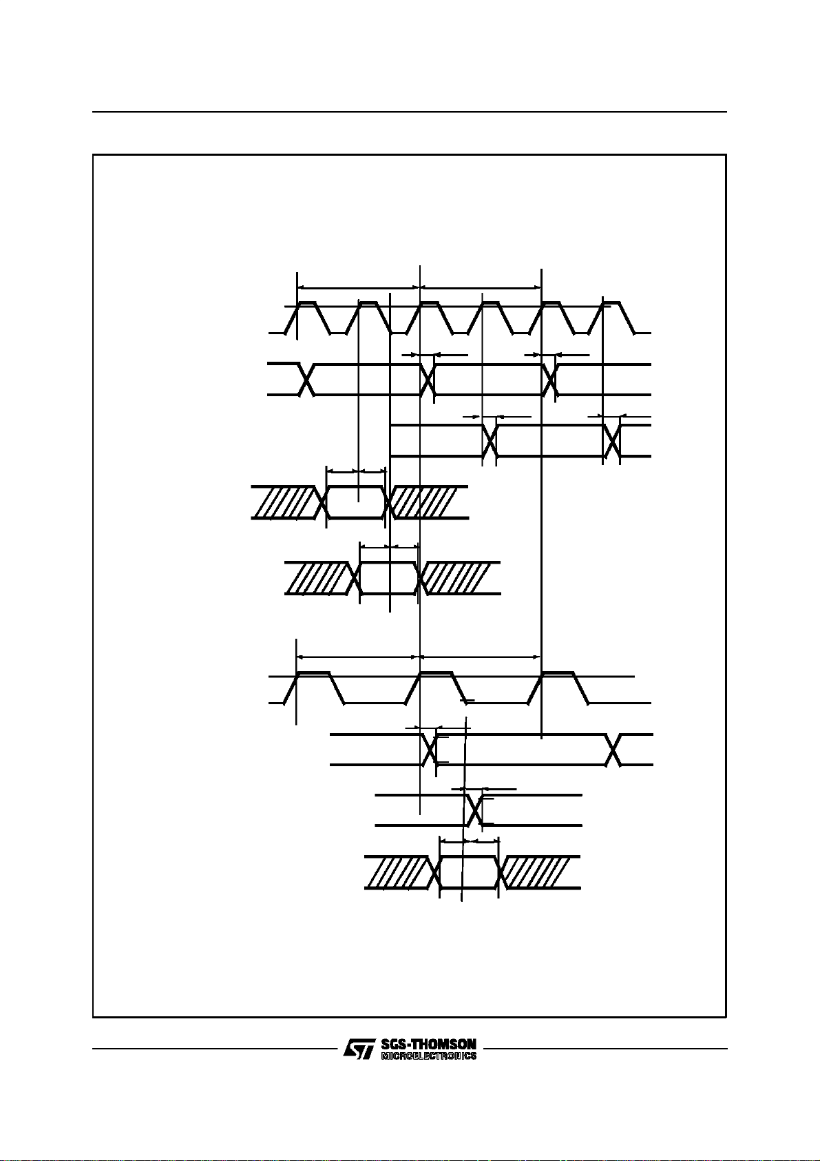
CLOCK TIMING
Synchronizationsignals delivered by the system
PDC
PFS
TXD0/3
RXD0/3
TS0/3
Bit3
Bit4
Bit5
Bit6
t6
t1t5h t5l
t7 t8
7610543
Bit7
t2
t3 t4
Bit0
Bit1
TDM0/3
FSC delivered
by the circuit
DEL, ISPP and PFSP bits of PCM Configuration Register are at zero (no delay))
Time Slot 31 Time Slot 0
Clocks receivedby the LCIC
tx Parameter T min. T typ. T max. Unit
t1=1/f1 Clock Period if f1 = 16384KHz
Clock Period if f1 = 8192KHz
Clock Period if f1 = 4096KHz
t2 Bit-time if f1 = 16384KHz
Bit-time if f1 = 8192KHz
Bit-time if f1 = 4096KHz
t3 Set up time PFS/PDC 20 t1-20 ns
t4 Hold time PFS/PDC 20 12500-t1 ns
t5 Clock ratio t5h/t5l 75 100 125 %
t6 PDC to data 50pF
PDC to data 100pF
t7 Set up time data/DCL 20 ns
t8 Hold time data/DCL 20 ns
60
120
239
61
122
244
122
244
488
62
124
249
50
100
ns
ns
ns
ns
ns
ns
ns
ns
36/54
Page 37

CLOCK TIMING
TDM synchronization
PDC received by
the LCIC
t2
STLC5460
t1
DCL delivered by
the LCIC
FSC delivered by
the LCIC
t3
t4
t5
t6
DOUT 0/1
Bit7, Time Slot 31
Bit0, Time Slot 0
t7 t8
DIN 0/1
The four Multiplex Configuration Registers are at zero (no delay between FSC and Multiplexes)
Clocks deliveredby the LCIC
tx Parameter T min. T typ. T max. Unit
t1 Clock Period if 4096KHz
Clock Period if 2048KHz
t2 Delay between PDC andDCL (30pF) 5 30 ns
t3 Delay between DCL and rising edge FSC (30pF) 30 ns
t4 Delay between DCL and falling edge FSC (30pF) 30 ns
t5 Duration FSC 488 ns
t6 DCL to data 50pF
DCL to data 100pF
t7 Set up time data/DCL 20 ns
t8 Hold time data/DCL 20 ns
Id PDC 244
488
Id PDC ns
50
100
ns
ns
ns
37/54
Page 38

STLC5460
DC SPECIFICATION
Absolute Maximum Ratings
Symbol Parameter Value Unit
V
T
Power Dissipation
Symbol Parameter Test Condition Min. Typ. Max. Unit
RecommendedDC OperatingConditions
Symbol Parameter Test Condition Min. Typ. Max. Unit
V
T
oper
Note 1: All the following specifications are valid only within these recommended operating conditions.
TTL Input DC ElectricalCharacteristics
5V Power Supply Voltage -0.5 to 6.5 V
DD
Input or Output Voltage -0.5,VDD +0.5 V
Storage Temperature -55, +125 °C
stg
P Power Consumption V
5V Power Supply Voltage 4.75 5.25 mW
DD
= 5.25V 105 135 mW
DD
Operating Temperature -40 +85 °C
Symbol Parameter Test Condition Min. Typ. Max. Unit
V
V
I
I
I
IH_PULLUP
C
C
OUT
C
Note 2: Excluding package
Low Level Input Voltage 0.8 V
IL
High Level Input Voltage 2.0 V
IH
Low Level Input Current VI=0V 1
IL
High Lvel Input Vi=V
IH
High level input current for pullup Vi = V
Input Capacitance (see Note 2) f = 1MHz @0V 2 4 pF
IN
DD Max
DD Max
Output Capacitance 4 pF
Bidir I/O Capacitance 4 8 pF
I/O
-1
-50
CMOS Output DC ElectricalCharacteristics
Symbol Parameter Test Condition Min. Typ. Max. Unit
V
V
Low Level Output Voltage IOL= 4mA
OL
High Level Output Voltage IOH= 4mA
OH
I
OL
I
OH
= 2mA
= 4mA
0.5
0.4
-0.5
V
DD
V
-0.4
DD
Protection
Symbol Parameter Test Condition Min. Typ. Max. Unit
V
ESD
Electrostatic Protection C = 100pF, R = 1.5kΩ 2000 V
A
µ
A
µ
A
µ
V
V
38/54
Page 39

APPENDIX
MEMORY ACCESSES
COMMAND MEMORY ACCESSES. CM=1
Write
CommandMemory:
CMD and SRC registersare writtenif their bits have not the right value.
CMD and SRC registerscan bewritten in any order.
DST registeris always written the last
CMD SRC DST
STLC5460
RCM
01
R=0 Write
CM=1 Command
Memory
Read CommandMemory in two steps:
Firststep: register writing
Subchannel select
and data rate
6
IN
CommandMemory
194 words of 14 bits
CMD register is written if its bits are not the right value.
SRC registeris notwritten.
DST registeris alwayswritten the last.
CMD SRC DST
R
CM
1
1
bits not used
2
1 of 192 input timeslots
1 of 2 insert registers
88
IN
Register not writte
n
1 of 192 output timeslots
1 of 2 extractregisters
A
1 of 192 output timeslots
1 of 2 extract register
8
OUT
R CM selected channel
1 1 and data rate
CMD SRC DST
Secondstep: registerreading:
CMD and SRCregisters may be readin any order.
DST registeris notchanged.
Command Memory
194 words of 14 bits
OUT
86
1 of 192 input timeslots
1 of 2 insertregisters
A
1 of 192 outputtimeslot
s
1 of 2 extract registers
39/54
Page 40

STLC5460
AUXILIARYMEMORYACCESSES:CM=0
Write Auxiliary Memory: Transmit command / indicatechannels
CMD and SRC registers arewritten if their bitshave not the right value.
CMD and SRC registers can be written in any order.
DSTregister is always written the last.
CMD SRC DST
RCM
Bits not used
00
R=0 Write
Primitive to transmit
4or6
MON TX
01
CM=0 Auxiliary Memory
IN
AUXILIARY MEMORY
16 words assigned to
8 TX C/I channels of MUX0
&
8 TX C/I channels of MUX1
Read AuxiliaryMemory in two steps: Transmitcommand / indicatechannels
Firststep: register writing:
CMD register is written if its bits are not the right value.
SRC registeris notwritten.
DST registeris alwayswritten the last.
CMD SRC DST
RCM
1
0
bits not used
Register not writte
A
MON TX
01
1 of 16 TX C/I
channels
6
1of16TXC/I
channels
2
RCM
10
Secondstep: registerreading:
40/54
C/I channel status
CMD SRC DST
CMD and SRC registersmay be readin any order.
DST registeris not changed.
n
AUXILIARY MEMORY
16 words assigned to
8 TX C/I channels of MUX0
&
8 TX C/I channels of MUX1
OUT OUT
2
4or6
channel status & Primitive
which has been transmitted
A
MON TX
01
6
1of16TXC/I
channels
Page 41

AUXILIARYMEMORYACCESSES:CM=0
Write Auxiliary Memory: Receive command / indicate channels
CMD and SRC registersare writtenif their bits have not the right value.
CMD and SRC registerscan bewritten in any order.
DST registeris always written the last.
CMD SRC DST
STLC5460
RCM
00
R=0 Write
CM=0 Auxiliary Memory
Read
AuxiliaryMemory in two steps:
Firststep: register writing:
Bits not used
CMD SRC DST
RCM
10
bits not used
Primitiveto initiate
4or6
N
AUXILIARY MEMORY
16 words assigned to
8 RX C/I channels of MUX0
8 RX C/I channels of MUX1
Receive command / indicate
CMD register is written if its bits are not the right value.
SRC registeris notwritten.
DST registeris alwayswritten the last.
I
&
Register not written
MON TX
00
A
channels
MON TX
00
1 of 16 TX C/I
channels
6
1of16TXC/I
channels
2
RCM
10
channel status
CMD SRC DST
Secondstep: registerreading:
CMD and SRCregisters may be readin any order.
DST registeris notchanged.
AUXILIARYMEMORY
16 words assigned to
8 RXC/I channels of MUX0
&
8 RXC/I channels of MUX1
OUT OUT
2
4or6
channel status & Primitive
which has been received
6
A
MON TX 1 of 16 TX C/I
0 0 channels
41/54
Page 42

STLC5460
AUXILIARYMEMORYACCESSES:CM=0
Write Auxiliary Memory: Transmit Monitor channels
CMD and SRC registersare writtenif their bits have not the right value.
CMD and SRC registerscan bewritten in any order.
DST registeris always written the last.
CMD SRC DST
RCM
00
Command bits
R=0 Write
CM=0 Auxiliary Memory
Read
Auxiliary Memory in two steps:
Firststep: register writing:
CMD register is written if its bits are not the right value.
SRC registeris notwritten.
DST registeris alwayswritten the last.
CMD SRC DST
RCM
10
bits not used
Data to transmit
8
IN IN
AUXILIARYMEMORY
16 words assigned to
8 TX MON channels of MUX0
&
8 TX MON channels of MUX1
TransmitMonitor
Register not written
channels
MON TX
11
1 of 16 TX MON
channels
63
A
MON TX 1 of 16 TX MON
1 1 channels
42/54
2
R CM MON status
10
CMD SRC DST
Secondstep: registerreading:
CMD and SRCregisters may be readin any order.
DST registeris notchanged.
AUXILIARY MEMORY
16 words assigned to
8 TX MON channels of MUX0
&
8 TX MON channels of MUX1
OUT OUT
5
8
data which has been
transmitted
6
A
MON TX 1 of 16 TX MON
1 1 channels
Page 43

AUXILIARYMEMORYACCESSES:CM=0
Write Auxiliary Memory: Receive Monitor channels
CMD and SRC registersare writtenif their bits have not the right value.
CMD and SRC registerscan bewritten in any order.
DST registeris always written the last.
CMD SRC DST
STLC5460
RCM
00
R=0 Write
Not used
Data to initiate
8
CM=0 Auxiliary Memory
IN
AUXILIARY MEMORY
16 words assigned to
8 RX MON channels of MUX 0
&
8 RX MON channels of MUX 1
Read AuxiliaryMemory in two steps: Receive Monitor channels
Firststep: register writing:
CMD register is written if its bits are not the right value.
SRC registeris notwritten.
DST registeris alwayswritten the last.
CMD SRC DST
CM
R
10
bits not used
Register not written
MON TX
10
A
MON TX
10
1of16TXMON
channels
6
1of16TXMON
channels
2
RCM
10
Secondstep, registerreading:
MON status
CMD SRC DST
CMD and SRCregisters may be readin any order.
DST registeris notchanged.
AUXILIARY MEMORY
16 words assigned to
8 RX MON channels of MUX0
&
8 RX MON channels of MUX1
OUT OUT
3
8
data which has been
received
6
A
MON TX 1 of 16 TX MON
1 0 channels
43/54
Page 44

STLC5460
Table 1: Data Memory Address
INPUT
PCM N1 N0 TS4 TS3 TS2 TS1 TS0
PCM 0
PCM 1 01 TS0toTS31
1
00 TS0toTS31
Source Register
PCM 2 10 TS0toTS31
PCM 3 11 TS0toTS31
MUX 0
MUX 1 1 TS 0 to TS 31
0
INSERT REG. A
0
1
0 TS 0 to TS 31
000000
INSERT REG. B 000001
Table 2:
ControlMemory Address
INPUT
Destination Register
PCM N1 N0 TS4 TS3 TS2 TS1 TS0
PCM 0
PCM 1 01 TS0toTS31
1
00 TS0toTS31
PCM 2 10 TS0toTS31
PCM 3 11 TS0toTS31
MUX 0
MUX 1 1 TS 0 to TS 31
0
EXTRACT REG. A
0
1
0 TS 0 to TS 31
000000
EXTRACT REG. B 000001
44/54
Page 45

Table 3: AuxiliaryMemory Addresss
STLC5460
MUX CHANNEL
CI
MUX 0
MON
CI
MUX 1
MON
- MON TX - M0 G2 G1 G0
RX
TX 0 1 GCI channel 0 to 7
RX 1 0 GCI channel 0 to 7
TX 1 1 GCI channel 0 to 7
RX 0 0
TX 0 1 GCI channel 0 to 7
RX 1 0 GCI channel 0 to 7
TX 1 1 GCI channel 0 to 7
00
Destination Register
GCI channel 0 to 7
0
GCI channel 0 to 7
1
Table 4: AuxiliaryMemory Data
CHANNEL Source Register
TX Command Indicate - - C6 C5 C4 C3 C2 C1
RX Command Indicate OVR PR C6 C5 C4 C3 C2 C1
TX and RX Monitor M8 M7 M6 M5 M4 M3 M2 M1
C1/6: Primitive
PR: Primitive received
OVR: Overrun
M1/8: Byte
45/54
Page 46

STLC5460
MEMORY ACCESS ALGORITHM
Figure 4: Controlor Auxiliary Memory Accesses
WRITE MEMORY
Read Status Register
Read Status Register
BUSY
Yes
No
Write Command Register
w ith R/W=0
Write So urce Regis ter
Write Destination Reg ister
END
READ MEMORY
Read Status Register
Read Status Register
BUSY
Yes
No
Write Command Register
with R/W=1
Write Destination Registe r
Read Status RegisterRead Status Register
46/54
BUSY
Yes
No
Rea d Comm and Regis ter
(optiona l)
Read Sou rce Register
Read Des tination Regis ter
(op t ional)
END
Page 47

Figure 5: BidirectionalSwitching
Ex 1: Source Register 1 1 0 0 0 0 1 1
Destination Register 0 0 1 0 1 1 0 1
Simple switching (BID=0)
The output MUX 1-TS 13 receives the contents of the input PCM 2-TS 3
Bidirectional switching (BID=1)
STLC5460
CHANNELS AT 64kbit/s
PCM 2 TS 3
MUX 1 TS 13
(or MUX 1 B2 of GCI 3)
The output MUX 1-TS 13 receives the contents of the input PCM2-TS 3
AND
The output PCM 2-TS 3 receives the contents of the input MUX 1-TS 13
Ex 2: Source Register 0 1 0 0 0 0 0 0
Insert Register A
Destination Register 0 0 101101
MUX 1 TS 13
(or MUX 1 B2 of GCI 3)
Simple switching (BID=0)
The output MUX 1-TS 13 receives the contents of the Insert Register A
Bidirectional switching (BID=1)
The output MUX 1-TS 13 receives the contents of the Insert Register A
AND
The Extract Register A receives the contents of the input MUX 1-TS 13
47/54
Page 48

STLC5460
Figure 6: BidirectionalSwitching and Loopback
Ex3: Source Register 0 1 0 0 0 0 0 0
Destination Register 0 1 0 0 0 0 0 1
Simple switching (BID=0)
The Extract Register B receivesthe contents of the InsertRegister A
Bidirectional switching (BID=1)
Insert Register A
Extract Register B
The Extract Register B receivesthe contents of the InsertRegister A
AND
The Extract Register A receivesthe contents of the Insert Register B
Ex 4: SourceRegister 1 0 1 1 0 1 0 1
PCM 1 TS 21
Destination Register 10100111
PCM 1 TS 7
Simple switching (BID=0)
The output PCM 1-TS 7 receives the contentsof the input PCM 1-TS 21
This is a loopback
Bidirectional switching (BID=1)
The output PCM 1-TS 7 receivesthe contents of the input PCM 1-TS21
AND
The output PCM 1-TS 21receivesthe contents of the input PCM 1-TS 7
Two loopbacks are established
48/54
Page 49

Figure 7: Switching& Broadcast
Ex 5:PCM to MUX
STLC5460
One source to severaldestinations
Source Register
10100010
PCM 1 TS 2
DestinationRegister 0 0 1 0 1 1 0 1
MUX 1 TS 13
(or MUX 1 B2 of GCI 3)
DestinationRegister 0 0 0 1 1 0 0 1
MUX 0 TS 25
(or MUX 0 B2 of GCI 6)
Broadcast
The output MUX1-TS 13 receivesthe contents of the input PCM 1-TS 2
AND
The output MUX 0-TS25 receives the contents of the input PCM 1-TS2
andso on
Ex 6:Insert Register A to MUX
Source Register
01000000
Insert RegisterA
Destination Register 0 0 0 1 1 1 0 0
MUX 0 TS 28
(or MUX 0 B1 of GCI7)
Destination Register
00110101
MUX 1 TS 21
(or MUX 1 B2 of GCI 5)
Broadcast
The output MUX 0-TS28 receives the contents of the Insert Register A
AND
The output MUX1-TS 21 receivesthe contents of the Insert Register A
49/54
Page 50

STLC5460
Figure 8: BidirectionalSwitching Channelsat 16kbit/s
Ex7: Channel at 16 kbit/s
Command Register
Source Register
PCM 2 TS 3
Destination Register 00101101
MUX 1 TS 13
(or MUX 1 B2 of GCI 3)
Simple switching (BID=0)
The output MUX 1-TS13 (bits 4-5) receives the contents of the input PCM 2-TS 3 (bits 2-3)
01011001
RCM CH SS DS
11000011
Bidirectionalswitching (BID=1)
The output MUX 1-TS13 (bits 4-5) receives the contents of the inputPCM 2-TS 3 (bits2-3)
the output PCM 2-TS 3 (bits 2-3) receivesthe contents of theinput MUX 1-TS 13 (bits 4-5)
AND
Ex8:Channel at 16 kbit/s(Insert register)
Command Register
01010001
RCMCH SS DS
Source Register
01000000
Insert RegisterA
Destination Register 00101101
MUX 1 TS 13
Simple switching(BID=0)
The output MUX 1-TS 13 (bits 4-5) receives the contents of the Insert Register A bits 6-7.
(or MUX 1 B2 of GCI 3)
Bidirectionalswitching (BID=1)
The output MUX 1-TS13 (bits 4-5) receives the contents of the Insert Register A bits 6-7 AND
the Extract Register A (bits6-7) receivesthe contents of theinput MUX 1-TS 13 (bits 4-5).
R Read;CM Command Memor y;CH Channel;SS Source Subchannel; DS Destination Subchannel
50/54
Page 51

Figure 9: BidirectionalSwitching Channelsat 32kbit/s
Ex 9: Channels at 32 kbit/s
STLC5460
Command Register
01 100100
RCMCH SS DS
Source Register
11110011
PCM 3 TS 1 9
Destination Register
00111101
MUX 1 TS 29
(or MUX 1 B2 of GCI 7)
Simple switching
The output MUX 1-TS 29 (bits 4 to 7) receivesthe contents of the input PCM 3-TS19 (bits 0 to 3)
Bidirectional switching
The output MUX 1-TS 29 (bits 4 to 7) receives the contents of the input PCM 3-TS19 (bits 0 to 3)
The output PCM 3-TS19 (bits 0 to 3) receivesthe contents of the input MUX 1-TS 29 (bits 4 to 7)
(BID=0)
(BID=1)
AND
Ex: 10: Channels at 32 kbit/s (Insert register)
Command Register
0 1100000
RCMCH SS DS
Source Register
01000000
Insert Register A
Destination Register
0 0101101
MUX 1 TS 13
Simple switching (BID=0)
The output MUX 1-TS AND 13 (bits4 to 7) receives the contents of the Insert Register A (bits 4 to 7).
Bidirectional switching
The output MUX 1-TS 13 (bits 4 to 7) receivesthe contents of the Insert Register A bits (4 to 7)
the Extract Register A bits(4 to 7) receives the contents of the input MUX 1-TS 13 bits (4 to7).
R Rea d; CM Command Memory; CH Chan nel; SS Source Subchan nel; DS Destination Subcha nn el
(BID=1)
(or MUX 1 B2 of GCI 3)
AND
51/54
Page 52

STLC5460
INTERRUPTEXAMPLE
Figure 10: InterruptGeneratedby RX Monitor Channel.
Interrupt
Yes
Read Interrupt Register
MONR=1
No
Re ad Rec eiv e MON Status Re gis ter
to kno w the num ber of th e ch an ne l
w h ich ha s ge ne rated th e Interrupt
and the Status Bits associated.
Byte=1
No
Yes
Read AuxiliaryMemory w ith
RX MON channel number into
Destination Re gister
The byte received is into
Sou rce Reg is ter
52/54
END
Page 53

PLCC44 PACKAGE MECHANICAL DATA
STLC5460
DIM.
MIN. TYP. MAX. MIN. TYP. MAX.
A 17.4 17.65 0.685 0.695
B 16.51 16.65 0.650 0.656
C 3.65 3.7 0.144 0.146
D 4.2 4.57 0.165 0.180
d1 2.59 2.74 0.102 0.108
d2 0.68 0.027
E 14.99 16 0.590 0.630
e 1.27 0.050
e3 12.7 0.500
F 0.46 0.018
F1 0.71 0.028
G 0.101 0.004
M 1.16 0.046
M1 1.14 0.045
mm inch
53/54
Page 54

STLC5460
Information furnished is believed to be accurate and reliable. However, SGS-THOMSON Microelectronics assumes no responsibility for the
consequences of use of such information nor for any infringement of patents or other rights of third parties which may result from its use. No
license is granted by implication or otherwise under any patent or patent rights of SGS-THOMSON Microelectronics. Specification mentioned
in this publication are subject to change without notice. This publication supersedes and replaces all information previously supplied.
SGS-THOMSON Microelectronics products are not authorized for useas criticalcomponentsin lifesupport devices or systems withoutexpress
written approval of SGS-THOMSON Microelectronics.
1997 SGS-THOMSON Microelectronics– Printed in Italy – AllRights Reserved
SGS-THOMSON Microelectronics GROUP OF COMPANIES
Australia - Brazil - Canada- China - France - Germany - HongKong - Italy- Japan - Korea - Malaysia - Malta - Morocco - The Netherlands -
Singapore - Spain - Sweden - Switzerland - Taiwan - Thailand - United Kingdom - U.S.A.
54/54
 Loading...