

Page 1
QUAD LINE FEED CONTROLLER
■ BATTERY VOLTAGE UP TO 120V
■ SUPPLIES POWE R FOR UP TO FOUR
DIGITAL TELEPHONE LINES
■ PROGRAMMABLE CURRENT LIMITING
■ LONGITUDINAL CURRENT CANCELLATION
■ ETSI ETR80 COMPL IAN T
■ OUTPUT CURRENT UP TO 140 mA
■ STATUS CONDITION DETECTION FOR
EACH LINE
■ AUTOMATIC THERMAL PROTECTION
■ AUTO POWER ON SEQUENCE
■ OUTPUT STAGE OPTIMIZED FOR MINIMAL
OUTPUT OVERVOLTAGE PROTECTION
■ TWO EXTERNAL RELAY DRIVERS PER LINE
■ PARALLEL OR MPI CONTROL INTERFACE
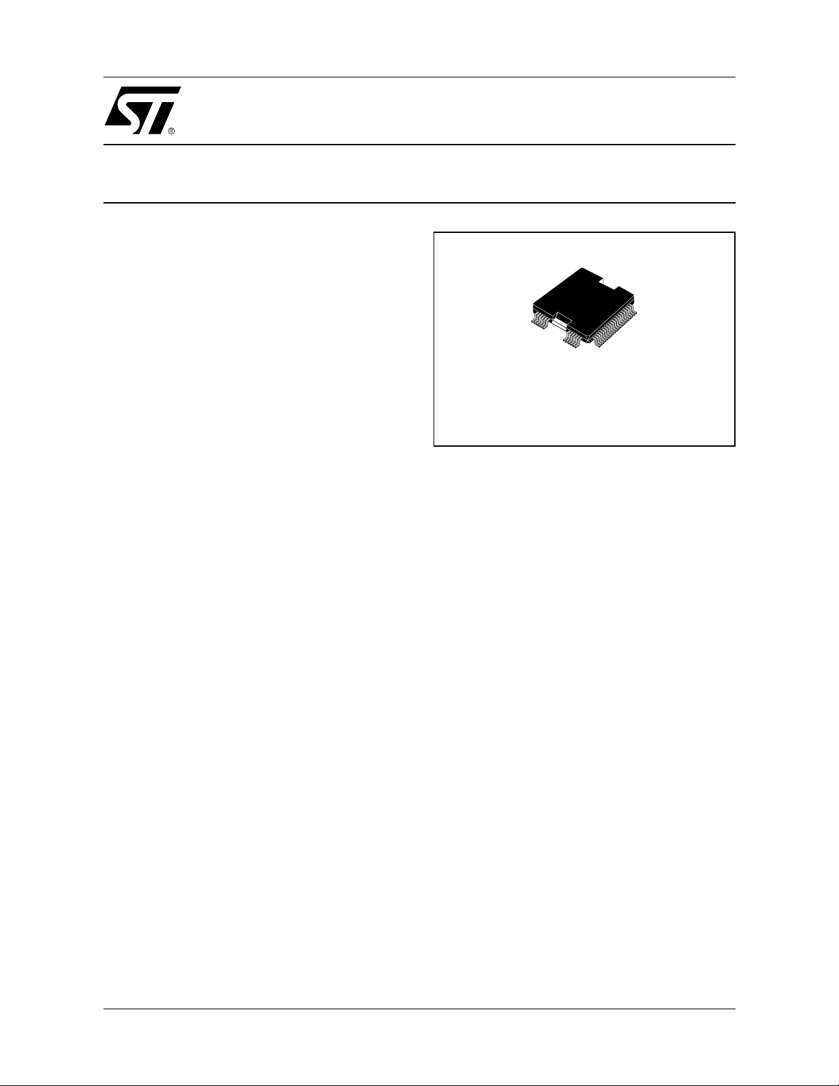
■ HI-QUAD PACKAGE 64 PIN
DESCRIPTION
The QUAD LINE FEED CONTROLLER provides a
power source for up to four U line interfaces. The
power source to the device is a local battery or a centralized regulated power supply. Each powered line is
individually controll ed and monitored by the device
interface.
A MPI or a simple parallel interface can be selected
STLC5445
HiQUAD-64
ORDERING NUM BER: STLC 5445
by a pin strap.
Each line can be individually powered and monitored:
therefore overload and faults can easi ly be detected
and localized even in a large system. The status conditions detected by the device are: Current Overload,
Thermal Overload, Open Loop. If activated (by
means of a dedicated pin strap), a self generated
power on sequence avoids the thermal over stress
when a simultaneous power on has been r equested
for more than one channel. The current limiting value
can globally be programmed for the four channels by
means of an external resistor. The device has two integrated relay drivers per line to drive the test relays
of the ISDN system.
October 2002
1/23
Page 2
STLC5445
BLOCK DIAGRAM
ILIM
110°C
PSC
PBIT
CKILC
RESETN
INTN
ALE
ES0 (A0)
ES1 (CSN)
ES2 (RDN)
ES3 (WRN)
NACK0 (D0)
NACK1 (D1)
NACK2 (D2)
NACK3 (D3)
Reference & biasing
generation
Thermal
monitoring
130°C
160°C
Logic
interface
Limiting
current
reference
Voltage
and
current
biasing
COD
OLD
Channel 3
Channel 2
Channe l 1
Channel 0
On / Off
&
line current
control
COD & OLD
generation
WBP0
WB0
WA0
V
BAT
CODC0
V
CC
VCC
BGND
EREL3B
DGND
EREL3A
EREL2B
RGND
VBAT
V
BAT
EREL2A
EREL1B
EREL1A
EREL0B
EREL0A
I / O conne ctions on channels 1, 2 and
3 are similar to those
shown for channel 0 but have been omitted for clarity
reasons.
Relay driver 3B
Relay driver 3A
Relay driver 2B
Relay driver 2A
Relay driver 1B
Relay driver 1A
Relay driver 0B
Relay driver 0A
Driving
&
output
clamping
REL3B
REL3A
REL2B
REL2A
REL1B
REL1A
REL0B
REL0A
2/23
Page 3
STLC5445
PIN CONNECTION
NACK0(D0)
NACK1(D1)
*EREL0A
*EREL0B
*EREL1A
*EREL1B
(Top view)
CODC0
CODC1
RGND
CK_ILC
REL0A
REL0B
REL1A
REL1B
ALE
PBIT
PSC
INTN
BGND
N.C.
WA0
BGND
63
64
1
2
3
4
5
6
7
8
9
10
12
13
14
15
16
17
18
19
20
21 22 23 24 25
62
VBAT
WB0
WBP0
RGND
60
61
59 58 57 56 55 54 53
26
VBAT
WB3
WBP3
ILIM
N.C.
271128 29 30 31 32
WA3
52
51
50
49
48
47
46
45
44
43
42
41
40
39
38
37
36
35
34
33
N.C.
BGND
*RESET
NACK3(D3)
NACK2(D2)
REL3B
*EREL3B
*EREL3A
REL3A
REL2B
*EREL2B
*EREL2A
REL2A
*ES3(WR)
*ES2(RD)
*ES1(CS)
*ES0(A0)
RGND
CODC3
CODC2
CC
V
N.C.
WA1
*INTERNAL PULL DOWN TO GROUND
WBP1
WB1
VBAT
VBAT
WB2
WBP2
DGND
WA2
BGND
D99TL437
PIN FUNCTION
N° Pin Name Description
1 CODC0 Pin for connection of the external capacitor (100nF/6.3V) to GND for COD signal filtering on
channel 0.
2 CODC1 Pin for connection of the external capacitor (100nF/6.3V) to GND for COD signal filtering on
channel 1
4 CKILC External clock input pin for the internal power on sequencer
5 NACK0(D0) Logic pin: with PSC = 0, Line 0 status information output
6 NACK1(D1) Logic pin: with PSC = 0, Line 1 status information output
7 REL0A Output of the 0A relay driver
8 *EREL0A Logic input pin: relay 0A output driver’s ON/OFF (high = ON)
9 *EREL0B Logic input pin: relay 0B output driver’s ON/OFF (high = ON)
10 REL0B Output of the 0B relay driver
with PSC = 1, Line 0 I/O tristate data bus
with PSC = 1, Line 1 I/O tristate data bus
11 REL1A Output of the 1A relay driver
3/23
Page 4
STLC5445
PIN FUNCTION
N° Pin Name Description
12 *EREL1A Logic input pin: relay 1A output driver’s ON/OFF (high = ON)
13 *EREL1B Logic input pin: relay 1B output driver’s ON/OFF (high = ON)
14 REL1B Output of the 1B relay driver
15 ALE Logic input pin: with PSC = 0, Don’t care
16 PBIT Power on sequencer enable: PBIT = 0: power on sequencer ON
17 PSC Parallel or MPI mode input selection pin:
18 INTN Logic output pin; open drain: with PSC = 0 high impedance
21 WA1 Output feeder’s switch side of line 1; negative respect to WB1
23 VCC Positive supply voltage. It is referred to DGND
24 WBP1 Internal protection diodes for line 1
25 WB1 Output feeder’s resistive side of line 1; positive respect to WA1
28 WB2 Output feeder’s resistive side of line 2; positive respect to WA2
(continued)
with PSC = 1, Address Latch Enable (active high)
PBIT = 1: power on sequencer OFF
0 = parallel interface; 1 = MPI interface
with PSC = 1 interrupt (active low)
29 WBP2 Internal protection diodes for line 2
30 DGND Digital ground
31 WA2 Output feeder’s switch side of line 2; negative respect to WB2
33 CODC2 Pin for connection of the external capacitor (100nF/6.3V) to GND for COD signal filtering on
channel 2
34 CODC3 Pin for connection of the external capacitor (100nF/6.3V) to GND for COD signal filtering on
channel 3
36 *ES0(A0) Logic input pin: with PSC = 0, Line 0 ON/OFF request (high=ON)
37 *ES1(CSN) Logic input pin: with PSC = 0, Line 1 ON/OFF request (high=ON)
38 *ES2(RDN) Logic input pin: with PSC = 0, Line 2 ON/OFF request (high=ON)
39 *ES3(WRN) Logic input pin: with PSC = 0, Line 3 ON/OFF request (high=ON)
40 REL2A Output of the 2A relay driver
41 *EREL2A Logic input pin: relay 2A output driver’s ON/OFF (high = ON)
42 *ERL2B Logic input pin: relay 2B output driver’s ON/OFF (high = ON)
43 REL2B Output of the 2B relay driver
with PSC = 1, Address bit for R/W operations
with PSC = 1, chip select (active low)
with PSC = 1, Read command (active low)
with PSC = 1, Write command (active low)
44 REL3A Output of the 3A relay driver
4/23
Page 5
STLC5445
PIN FUNCTION
N° Pin Name Description
45 *EREL3A Logic input pin: relay 3A output driver’s ON/OFF (high = ON)
46 *ERL3B Logic input pin: relay 3B output driver’s ON/OFF (high = ON)
47 REL3B Output of the 3B relay driver
48 NACK2 (D2) Logic pin: with PSC = 0, Line 2 status information output
49 NACK3 (D3) Logic pin: with PSC = 0 line 3 status information output
50 *RESETN Logic input pin: reset (active low)
53 WA3 Output feeder’s switch side of line 3; negative respect toWB3
55 ILIM Current limit programming input
56 WBP3 Internal protection diodes for line 3
57 WB3 Output feeder’s resistive side of line 3; positive respect to WA3
60 WB0 Output feeder’s resistive side of line 0; positive respect to WA0
61 WBP0 Internal protection diodes for line 0
0 WA0 Output feeder’s switch side of line 0; negative respect to WB0
(continued)
with PSC = 1, Line 2 I/O tristate data bus
with PSC = 1 line 3 I/O tristate data bus
26
27
58
59
19
32
51
64
3
35
62
* Internal pull down to ground
VBAT Negative battery supply voltage. It is referred to BGND
BGND Battery ground
RGND Relay ground
5/23
Page 6
STLC5445
ABSOLUTE MAXIMUM RATINGS
Symbol Parameter Value Unit
V
V
V
V
I
WBn
I
NEG
T
DD
CD
BB
BD
stg
Voltage from digital input to DGND – 0.5 to VCC + 0.5 V
Voltage from VCC to DGND – 0.4 to +7 V
Voltage from VBAT to BGND – 143 to + 0.4 V
Voltage from BGND to DGND – 3 to +0.5 V
AC Current into the WBn outputs
(WBPn not connected to GND
250 mA
peak
Negative current injected in the WAn outputs (-40 to +85°C) 50 mA
Storage temperature – 60 to 150 °C
RECOMMENDED OPERATING CONDITION
Symbol Parameter Test Condition Min. Typ. Max. Unit
VCC supply voltage 4.75 5.25 V
CC
V
BAT
supply voltage – 120 – 38 V
BAT
BGND/DGND voltage – 3 0.5 V
(1)
Programmable range of the
current limiting function
20 140 mA
V
V
I
LIMT
V
BGND
I
Relay
T
a normal
Relay driver current 70 mA
Ambient temperature normal
range
T
a extend ed
Ambient temperature extended
range
Max operating loop current 140 mA
External, short circuit resistive
MIN
R
I
loop
load from WAn to WBn
070°C
– 40 85 °C
55 W
6/23
Page 7
STLC5445
ELECTRICAL CHARACTERISTCS
Unless otherwise specified the below listed parameters' values are referred to the following conditions:
V
= –115V, VCC = 5V, R
BAT
range [0°C to 70°C]. The presence of an asterisk mark (*) indicates that the marked parameter must remain
within the specified tolerance in the extended temperature range [-40°C to 85°C].
Symbol Parameter Test Condition Min. Typ. Max. Unit
= 53.6 kW, CODCn RC series = 100nF ±10% and 510Ω ±1%, normal temperature
lim
I
I
VBAT
I
LIMT
I
LIMTL
I
LIM%
R
R
∆R
T
Vcc
I
HZ
WA
WB
j110
VCC supply current All the switches on Νo load 2.5 mA
V
supply current All the switches on Νo load 1.5 1.8 mA
BAT
Current limiting value with
I
= 0 42.5 50 57.5 mA
long
transversal line current only
Current limiting value with added
See Fig.1 37.5 50 62.5 mA
longitudinal line current
Current limiting accuracy in the
range 20 to 140 mA
(1)
I
= 0 ±15 %
long
Leakage current of each WAn
output to ground with output
driver disabled
Resistance from WAn to
V
BAT
Resistance from WBn to
IWA = 30mA 3.15 5.5 7.85 Ω
IWB = 30mA 3.5 5.5 7.5 Ω
BGND
Absolute value of the difference
OUT
between R
R
WBn
and its related
WAn
110°C thermal monitoring
IWA = IWB = =30mA 0.7
110 °C
threshold
50* µA
Ω
1(*)
LV
V
V
I
T
j130
T
j160
T
hyst
out
Rel33
Rel70
Rleak
130°C thermal monitoring
130 °C
threshold
160°C thermal monitoring
160 °C
threshold
Thermal monitoring
10 °C
hysteresis
(2)
Longitudinal output component of
See Fig. 2 – 60 dBV
the fCKILC clock signal
Relay drivers’ output voltage All the relay drivers activated at a
load current of 33mA.
(3)
Relay drivers output voltage All the relay drivers activated at a
load current of 70mA.
(3)
Relay driver leakage current ERLn = Low 100 µA
0.5 V
1.2 V
7/23
Page 8

STLC5445
ELECTRICAL CHARACTERISTICS
Symbol Parameter Test Condition Min. Typ. Max. Unit
I
SOC
OLDH Open Loop detector Hysteresis 0.6 1.6 mA
Notes: 1. Our characterizations show that in t he range 15mA - 2 0mA the accuracy is ±20% over the 0°C - 70°C tempe rat ure range.
Open circuit detector threshold 1.5 3 4 mA
2. The longitudinal component of the signal detected by the spectrum analyzer must have an RMS voltage value, in any 4kHz equivalent ban dwi dth, ave rag ed in an y 1 seco nd peri od, not grea ter of the sp ecifi ed valu e (–6 0d BV) ove r the 100 Hz - 150kH z rang e
(for details see ETS I E TR80 and ANSI 601).
3. All th e output lines act i vated at a line c urrent of 35mA; no current limi tation conditi on. Rth(j-a ) ≤ 20°C/W
(continued)
Please note that, in order to assure the frequency stability of the output drivers, a 1µF capacitor must always
be connected between WAn and Wbn or, as shown in Fig. 6, immediately after the resistive protection elements
used in the actual application.
The R
value can be calculated starting from the value of the needed current limitation threshold I
LIM
R
LIM
2664
---------------=
I
LIMIT
LIMT
:
SWITCHING TIMING
Symbol Parameter Test Condition Min. Typ. Max. Unit
t
ENP
t
DISP
f
CKILC
Output driver’s enable time Parallel interface mode 20 µs
Output driver’s disable time Parallel interface mode 500 µs
Frequency of CKILC Duty cycle 60% max
Pulse width 500ns min
8 200 kHz
Figure 1.
WBn
STLC5445 output driver
(one of four)
WAn
Ω
25
±
0.01%
I
LIMTL
Ω
25
±
0.01%
Ω
30
±
0.01%
1.3kΩ ±1%
Ω
30
±
0.01%
20µF ±1%
20µF ±1%
8.5V
RMS
16.6Hz
8/23
Page 9

Figure 2.
STLC5445
67.5Ω
10µ F ±1%
±0.01%
WBn
STLC5445 output driver
(one of four)
3.9kΩ
±
1%
Spectrum analyzer
100Ω ±1%
WAn
67.5
±
0.01%
150nF ±10%
10µF ±1%
Ω
STATIC CHARACTERISTICS
Unless otherwise spe cified the below listed param eters values are referred to the following cond itions: VCC = 5V,
mal temperature range.
Symbol Parameter Test Condition Min. Typ. Max. Unit
V
Input low voltage 0.8 V
IL
nor-
V
V
V
I
I
I
Input high voltage 2 V
IH
Output low voltage Io = 1mA 0.4 V
OL
Output high voltage
OH
(Open drain with PSC = 0)
Input high current 0 1 0 µA
LH
Input low current -10 0 µA
LL
Output current in High impedance
OZ
state
Io = –1 mA 2.4 V
-10 10 µA
9/23
Page 10

STLC5445
SWITCHING CHARACTERISTICS
MICROPROCESSOR WRITE / READ TIMING
Unless otherwise specified the below listed parameters’ values are referred to the following conditions:
VCC=5V, normal temperature range.
Symbol Parameter Test Condition Min. Typ. Max. Unit
(refers to figures 3 and 4).
t
RLRH
t
RHRL
t
RLDA
t
RHDZ
t
AHAL
t
ADAL
t
ADAZ
t
AZRL
t
AZWL
t
ADDA
t
WLWH
t
WHWL
t
DAWH
t
WHDZ
RDN, CSN pulse width 260 ns
RDN, recovery time
T
= – 40 to 0°C and +70°C to +85°C
amb
200
220
ns
RDN, CSN low to data available 260 ns
RDN or CSN high to data Z
T
= – 40 to 0°C and +70°C to +85°C
amb
130
160
ns
ALE pulse width 100 ns
Address setup time 60 ns
Address hold time 50 ns
Address Z to RDN low 0 ns
Address Z to WRN Low 0 ns
Address stable to data available
T
= – 40 to 0°C and +70°C to +85°C
amb
360
390
ns
WRN or CSN pulse width 200 ns
Write recovery time 200 ns
Data setup time 100 ns
Data hold time
T
= – 40 to 0°C and +70°C to +85°C
amb
20
40
ns
t
RESN
10/23
Reset Pulse with 200 ns
Page 11

STLC5445
Figure 3. Microprocessor WRITE timing
t
ALE
A
O
CS
RD
Notes: 1. If tCLWL is negative tW LWH is measured from CS_ ra ther than fromWR_.
2. If tW HCH is negative, tWHWL, tWLWH, tDAWH and tWHDZ ar e measured fro m CS_ rather than fromWR_.
The propagation delay from the writing of the T/I bit to the effect on the INT pin is approximately 1ms for both ma sk and enable operatio ns.
AHAL
t
ADALtADAZ
t
ADDA
t
AZRL
t
CLRL
(Note 1)
t
RLDA
t
RLRH
t
RHCH
Read DataDATA
(Note 2)
t
RHDZ
t
RHRL
D94TL108A
Figure 4. Microprocessor READ timing
t
ALE
A
O
CS
WR
INT
Notes: 1. If tCLRL is negative, tRHRL, tRLRH , tAZRL, and tRLDA are meas ured from CS _ rat h er than RD_.
2. If tR HCH is negative, tRHRL, tRLRH and tRHDZ are measured from CS_ rather than RD_.
When a read from the LER immediately follows a write to the LER a minimum of 1ms is required between these operations
AHAL
t
ADALtADAZ
t
CLWL
(Note 1)
t
AZWL
t
WLWH
t
DAWH
Write DataDATA
t
WHCH
t
WHDZ
(Note 2)
(Note 3)
t
WHWL
D94TL109A
11/23
Page 12

STLC5445
Figure 5. Typical Application Circuit
Z1
2 x SM6T68A
C4 100nF
VBAT
RELAYS
COMAND
RELAYS
C3 100nF
C2 100nF
C1 100nF
VBAT
BGND
VBAT
BGND
VBAT
BGND
VBAT
EREL0A
EREL0B
EREL1A
EREL1B
EREL2A
EREL2B
EREL3A
EREL3B
REL0A
REL0B
REL1A
REL1B
REL2A
REL2B
REL3A
REL3B
N.C.
59
51
58
32
27
19
26
8
9
12
13
41
42
45
46
7
10
11
14
40
43
44
47
20,22,52,54
RGND V
C5
100nF
BGND
CC
ILIMDGND
64
235,35,62
CODC0 CODC1 CODC2 CODC3
C6
100nFC7100nFC8100nFC9100nF
5530
343321
50
4
18
17
16
15
36
37
38
39
5
6
48
49
61
24
29
56
60
25
28
57
63
21
31
53
RESET
CK_ILC
INTN
PSC
PBIT
ALE
ES0/A0
ES1/CS
ES2/RD
ES3/WR
NACK0(D0)
NACK1(D1)
NACK2(D2)
NACK3(D3)
WBP_0
WBP_1
WBP_2
WBP_3
WB_0
WB_1
WB_2
WB_3
WA_0
WA_1
WA_2
WA_3
JP0
JP1
JP2
JP3
D99TL440
DIGITAL
CONTROL
OUTPUTS
CLAMPING
DRIVER
OUTPUTS
External Component List
Coponents Description Value
C1, C2, C3, C4 & C5 Power Supply Filter Capacitance 100nF
C6, C7, C8 & C9 Signal Filter Capacitance 100nF
Programmable Limiting Current Resistor 53.6kΩ
Transil Clamping Protection 136V
12/23
R
LIN
Z
1
Page 13

Figure 6. Typical Protection Diagram (only channel 0 and 1 shown )
STLC5445
TIP
SM5908
16ΩPTC
1µF
RING
2 x
SM6T68A
W
BAT
TIP
1µF
RING
Note: The 1µF capacitors are required for output driver's stability
16ΩPTC
16ΩPTC
16ΩPTC
22Ω
22Ω
SM5908
22Ω
22Ω
D02TL549
B
GND
W
BP1
W
B1
CHANNEL's 1 OUTPUT
W
A1
W
BAT
B
GND
W
BP0
W
B0
W
A0
W
BAT
DRIVER's STAGE
CHANNEL's 0 OUTPUT
DRIVER's STAGE
FUNC TIONAL DESCRIPTION
(n=0-3) Drivers (output pins).
WAn
Each WAn output can sink up to 140mA. When the ESn input is High and the activation request
is approved by the internal control circui t ry, the respecti ve WAn output is internall y connected
to VBAT through a DMOS switch and the low side sensing resistor.
WBn
(n=0-3) Resistor to BGND.
Each WBn output connects the wire B to ground through a 5W resistor used to perform the
longitudinal balance and the high side current sensing function.
WBPn
(n=0-3) Protection diodes connection (see the block diagram at page 3).
Each channel of the STLC5445 has two internal, back to back connected diodes, whose clamping action can be used to protect t he WBn outputs during l ighti ng and power crossi ng events.
The diodes' clamping action is normally disabled and can be activated by connecting the WBPn
pin to BGND. In this case however, if the line current exceeds 57.5mA the forward drop across
the high side sensing resistor (and then across the diodes) reaches the diodes' conduction
threshold, strongly degrading the current l imiting action and the longi tudinal balance. For line
currents higher than 57.5mA external clamping elements must then be connected in place of
the internal diodes or in series to them in order to increase the clamping voltage value.
BGND
DGND
Battery ground.
Digital ground.
13/23
Page 14

STLC5445
RGND
CKILC
Logic input.
Ground connection of the relay drivers.
External clock input for the
block diagram at page 3). The Power On Sequencer controls (if activated) the power on sequence of the lines. Thi s will limit the chip's t emperature increase that occurs, at channels
switch on, due to the charging current of the capacitances used by the external ISDN circuitry.
If used, the Power on sequencer is the only block of the circuit that needs an external clock signal.
ESn
(n=0-3) Logic inputs.
These pins have double names (see the block diagram at page 3) because they perform a double function: one in
In Parallel mode ESn acts as an activation or deactivation request for the respective line driver:
In MPI mode the pins perform the following functions:
RESETN
Reset pin. It initializes the Power on sequencer, the TOR register and, in the MPI interface, the
registers and the INTN (interrupt output pin). When applied it leaves all the line drivers switched
off.
It has no effect in Parallel interface mode if the power on sequencer is not used.
When the supply voltages are applied t o the ci rcuit, an equival ent RESETN pulse (power on
reset) is automatically, internally generated.
ALE A
ddress Latch Enable. ALE is a logic input pin. It is used to strobe the address bit applied at
the A0 pin, into the address latch. The address is latched on the H igh to Low transition of ALE.
While ALE is High the address latch is transparent. For a non multiplexed microprocessor bus,
ALE must be tied High.
ILIM
The current limiting pr ogramming input, ILIM, is used to program the current limi t of the four
drivers by means of an external resistor connected between this pin and DGND. The voltage at
ILIM pin is a replica of the internal bandgap voltage (1.236V).
When a line driver is in current limitation, its output current is 2155 times higher than the current
flowing in the external current limiting programming resistor.
INTN
The INTN (interrupt) open drain type output can only be used in MPI interface mode. INTN can
be used to alerts an external microprocessor when a current overload condition occurs. It is not
Power On Sequencer
Parallel mode
( PSC = 0 ), and another in
ESn = 0: Line driver deactivation request.
ESn = 1: Line driver activation request.
A0:
Selects the source and destination locations for read and write operations on the
data bus. A0 must be valid on the falling edge of ALE or during RDN and WRN
if ALE is tied High. Data transfer occurs over the D0-D3 lines.
CSN:
This pin acts as a chip select. It must be Low to enable the read or write operations of the device.
RDN:
Read command. The active Low read signal is conditi oned by CSN and transfers internal information t o the data bus. If A0 is a logi cal 0, the logic lev els of
the
I
ndirect Address Register (
IAR
be transferred to D3-D0. If A0 is a logical 1, the data addressed by the
be transferred to D3-D0.
WRN:
Write command. The active Low write signal is conditioned by CSN and transfers information from the data bus to one of the two internal registers selectable
by A0: if A0 is a logical 1, D3-D0 is written into the
if A0 is a logical 0, D2-D0 are writt en into the
and D3 is written as bit 3 and manages the generation of the interrupt signal for
the external microprocessor.
LER
the device.
embedded in the
Logic interface
MPI mode
(see the
( PSC = 1).
) and of the Thermal Shutdown Status bit will
IAR
will
L
and
ine Enable Register (
I
ndirect Address Register (
IAR
are the only two writable registers in
LER
IAR
);
)
14/23
Page 15

STLC5445
latched and is active (Low level) when at least one of the CODn status detector bits is active
(High level). When the four CODn status detector bits are Low, INTN goes inactive (High). INTN
will also go inactive if (due to thermal overload) the QLFC automatically disables the output driver of the channel that caused the int errupt, or i f t he ext ernal microprocessor disabl es t hat li ne
via the Line Enable Register (LER). The interrupt function can be disabled (INTN remains permanently High) via the Indirect Address Register (IAR) or a Low level on the RESETN pin.
NACKn
PSC
ERLn
RLn
CODCn
(n=0-3) When a line over current condition exists, the output driver of the overloaded channel instanta-
(n=0-3)Logic I/O.
These pins have double names (see the block diagram at page 3) because they perform a double function: one in
Parallel mode
In
each NACKn acts as an open drai n output and gives the ch annel's status in-
formation.
The NACKn bit goes in high impedance state (bit = 1 if a NACKn pull up is provided) when at
least one of these conditions is verified:
The current on the relative line reaches the current limit programmed by the user.
The chip's temperature reach the thermal alarm threshold.
The line driver is in the Power on phase.
When the ESn input is set Low, the corresponding NACKn is set to zero.
In
MPI mode
the four pins become
capability. The four bidirectional data bus lines are used to exchange information with an external microprocessor. D0 is the least significant bit and D3 is the most significant bit. An High Level on the data bus corresponds to a logical 1. When the chip select bit (CSN) is Low, these lines
act as inputs when WRN is Low and as outputs when RDN is Low. When CSN is High the D3
- D0 pins are in a high impedance state.
Logic input.
This pin is used to select one of the two available logic interfaces.
PSC = 0: Parallel mode.
PSC = 1: MPI mode.
(n=0A-3B) Logic inputs.
Each ERLn pin controls directly the respective relay driver's DMOS:
ERLn = 0 : Switch off the relay driver.
ERLn = 1 : Switch on the relay driver.
(n=0A-3B) Relay drivers' output.
Each of the eight RLn pins is connected to the drain of an internal DMOS switch (see the block
diagram at page 3) which acts as a dri ver f or an ex ternal rel ay to be s uppl ied f rom VCC. The
relay drivers' current flows to ground through the RGND pins. Each output can sink up to 70
mA. An internal clamping circuit is provided, so no external kickback diodes are required.
neously limits the line current at the value programmed by means of the e xternal RLIM resistor.
In this condition the
When operating in MPI mode this bit can, for each of the four channels, be red by the external
microprocessor in order to check which channel (if any) is overloaded.
When in parallel mode each COD bit is internal l y OR combined with t wo other bi t s i n order t o
generate the NACKn bit.
Since in the ISDN application it can happens that the sum of the DC line current and the superimposed signal peaks, easily exceeds the needed DC current limit, the COD generation circuitry
has been arranged in such a way that the COD bit will be pushed H igh
load persists for at least 20ms: this eliminates any spurious High level COD / NACK. The men-
Parallel mode
C
urrent Overload Detector bit (COD) switches to a High logic level.
( PSC = 0 ), and another in
D3 - D0
and act as a bidirectional data bus with three state
MPI mode
only
( PSC = 1).
if the current over-
15/23
Page 16

STLC5445
tioned delaying function requires, for each of the four channels, one Capacitor of 100nF has to
be connected between each CODCn and ground.
OPERATIVE DESCRIPTION
The device compr ises t hree main blocks : the
The Analog section feeds the four lines and detects their status.
The Logic section allows to exchange information and commands between the QLFC and the external digital
system.
The Relay driver section is completely independent: each relay command input is related to its own driver with-
out any conditioning.
Analog section
, the
Logic section
and the
Relay driver section
.
Analog Section
The ANALOG section comprises the
and the
Thermal monitoring
(see the Block diagram at page 3)
Channel 0-Channel 3
block.
block, the
Reference & biasing generation
block
As shown in the channel's card of the block diagram, the WBn and WAn pins to which the line is connected are
respectively routed to the battery ground and to the VBAT line: WBn goes to BGND through the upper side sensing resistor; WAn goes to V BAT through a pow er DM OS a nd the lower side s ensing resistor. The ON/OFF control for the power DMOS comes from the outside world through the
Logic interface
block.
The implemented topology for the circuit used to cancel the longitudinal current effect is a DC coupled topology:
it doesn't need external capacitors and its frequency band starts from DC.
The QLFC has a double protection provided by its
current limiting
and
thermal monitoring capabilities
.
The current limit threshold (ILIMT) of the four channels is hardware programmable by means of a single, external resistor (RLIM):
I
LIMIT
1.236 2155⋅
--------------------------------=
R
.
LIM
The protection implemented by the thermal monitoring is based on a three levels control system:
A first temperature threshold controls the Power on sequencer (see the Logic Section for a detailed description of its behaviour). When activated (PBIT pin Low), the Power on sequencer
manages the channels' activation requests received through the Parallel (PSC pin Low) or the
MPI (PSC pin High) interface. The incoming channels' activation requests are stored in the
Power on sequencer and then satisfied, one at a time, only when the previously activated channel leaves the current limiting condition that normally occurs at power on, due to the capacitive
element that is part of the ISDN load. However when the chip's internal temperature reaches
110°C, only the already stored activation requests will be satisfied; the new, eventually incoming o nes , w ill be reje c te d and w ill be processed when the internal temperature decreases down
to 100°C.
A second temperature threshold is set at 130°C. When this value is reached the channels that
are in current limiting condition are switched off and their reactivation will only b e po s sible when
the chip's internal temperature has decreased down to 120°C or, if the Power on sequencer is
activated, down to 100°C.
The third temperature threshold is set at 160°C. When this temperature is reached the activated
channels will all be switched off and their r eacti vat ion will onl y be possible when the chip's i nternal temperature has decreased down to 150°C. The user must however take into account
that if (like in ISDN application) the load seen by the channel has a high capacitive component,
at channel's turn on a current limiting condition will alw ay s o ccu r a n d th e e ve ntu al ly r eac ti vat ed
channels will almost instantaneously be switched off by the 130°C monitoring circui t, if the
chip's internal temperature is still higher than 120°C. More over (as explained at the previous
point) if the Power on sequencer is activated it will not be poss ible to swit ch o n an y channel until
the chip has cooled down to 100°C.
16/23
Page 17

STLC5445
Each of the four channels generates two stat us detector bits ( see the block di agram at page 3): the COD bit
(
C
urrent Overload Detector) and the OLD bit (Open Loop Detector). The functions of the two bits are the follow-
ing:
The COD bit goes in a High logic state when its channel is in current limiting condition. Since in
the ISDN application it can happens that the sum of the DC line current and the superimposed
signal peaks, easily exceeds the needed DC current limit, the COD generation circuitry has
been arranged in such a way that the COD bit will be pushed High only if the current overload
persists for at least 20ms: this eliminates any spurious High level CO D. The mentioned delaying
function requires, for each of the four channels, one Capacitor of 100nF has to be connected
between each CODCn and ground.
The OLD bit goes in a High state logic when the current t hat the channel suppli es to the line
falls below a typical value of 3mA, indicating a probable open line condition.
As explained in the following pages, when operating in MPI mode the COD and OLD bits can, for each of the
four channels, be red by an ext ernal microprocessor i n order to check which channel (i f any ) is over or under
loaded. When in Parallel mode a single status bit (the NACKn bit) is provided for each channel and is di rec tly
available on a dedicated pin. The NACKn bit is internally generated by OR combining the COD bit with two other
bits (see the Logic section for a more detailed explanation).
Logic Section
The Logic section comprises the
block diagram shown at page 3 the three functions have been condensed in a single entity: the
Parallel interface
, the
MPI interface
and the
Power on sequencer
Logic interface
block.
For each of the four channels, both types of the two provided interfaces use the COD, OLD and TOR (
O
verload Register) status detector bits:
The COD (
C
urrent Overload Detector) bit is in a High logic state when its channel is in current
limiting condition since at least 20ms.
The OLD (
O
pen Loop Detector) bit is in a High logic state when the current that the channel
supplies to the line falls below a typical value of 3mA (ISOC spec's parameter), indicating a possible open line condition.
Each of the four output line drivers can be switched on,
only
if their corresponding TOR bit is
High.
The TOR bits are automatically set High by the internal power on reset when the chip is initially
connected to its power supplies but can, however, also be globally set High by applying a reset
pulse to the RESETN pin. Alternatively the TOR bits that are latched in a Low state can individually be set High by applying to the selected interface the switch off command relative to their
channel.
The T OR b its w ill go in a Lo w sta te ( de ter mining the shut off of t heir re lati ve c hannel's driver) in
two cases:
The activated channel is in current limiting condition and the chip's temperature reaches 130°C.
In this case the TOR will be latched in Low state.
The chip's temperature reaches 160°C: in this case the TOR bits wi ll all be set Low but only the
TOR of the activated channels will be latched.
. In the
T
hermal
Power on sequencer
When activated (PBIT pin Low), the Power on sequencer manages the channels' activation requests received
through the Parallel (PSC pin Low) or the MPI (PSC pin High) interface. The incoming channels' activation requests are stored in the Power on sequencer and then sati sfied, one at a t i me, onl y when the pr eviousl y acti vated channel exit the current limiting condition that normally occurs at power on, due to the capacitive element
that is part of the ISDN load. It must be noted that once a channel exits from the channel's turn on c urrent limiting
phase, the fact that it can for example because of a new line overload fal l again in a cur rent l imiti ng c onditi on
17/23
Page 18

STLC5445
has no influence in the activation sequence of the next channels. The stored activation requests are satisfied
starting from the lower index of the actually stored requests: if (for example) while channel 2 is in the activation
phase, additional power on requests arrive for (in the order) channels 1, 3 and 0, when the channel's 2 activation
phase will be conc luded the stored activation requests will be satisfied in the order 0, 1 and 3. It must be noted
that the channels' deactivation requests are not conditioned by the Power on sequencer.
Figure 7. Power on sequence exam ple
DAR0
COD0
POF0
DAR1
COD1
POF1
DAR2
COD2
POF2
Notes: D ARn are the line Drivers' Activation Request bits sent to t he Power on sequencer. They are internally generated sta rting from the
activatio n r eques ts c omin g f rom the outs ide w orl d thr ough t h e selec ted int erfa ce (P ar allel or MPI) . PO Fn a re th e Power On Flags.
Each POFn goes High with its relative DARn bit and returns to a Low state when the current limiting condition ends: a POF High state
indicates that the rel at iv e channel is in th e power on phase .
The figure 6 shows, for three of the four available channels, a typical power on sequence example. The COD n
pulse duration represents the time needed to charge the capacitive element that is part of the ISDN load, with
part of the constant current that each line driver provides with the actually programmed current limiting value. It
must be realized that if (for example) has been required the activation of the lines 0, 2 and 3 but line 2 is overloaded and cannot leave the current limiting condition, the activation sequence will rem ain blo ck ed at the line 2
activation step. In this case the external software has to identify and shut off the overloaded line in order to allow
the activation of the line 3.
The previously mentioned RESETN pin will also influence the Power on sequencer: when RESETN is pushed
Low the Power on sequencer is reset, switching off the actually activated drivers.
The Power on sequencer is the only block of the circuit that needs an external clock signal to be applied at the
CKILC pin. The clock frequency is not critical and has a nominal value of 8kHz.
When PBIT=1 the power on sequencer is disabled and the incoming channels' activation request s wil l instantaneously be satisfied. In this case the user as to take into account the actual operative condition (VBAT, the
programmed current limiting value, the load applied to the lines, the ambient temperature) and implement his
own power on sequence in order to li mit the chip' s temperature increas e induced by the c hannels' switch on
transients.
18/23
Page 19

STLC5445
Parallel interface mode
In Parallel interf ace mode (PSC pin Low), for each of the four output driv ers a dedi c ated act ivati on pi n i s provided (ES0-ES3):
Each driver will unconditionally be switched off when its ESn is pushed Low.
If the Power on sequencer is not used, each driver will b e switc hed on (under the s upervision of the pre-
viously described Thermal monitoring block) when its ESn is pushed High.
If the Power on sequencer is activated the drivers' activation requests coming from the ESn inputs will
(under the supervision of the previously described Thermal monitoring block) be processed by the Power on sequencer block (see the previous Power on sequencer's description).
In Parallel interface mode a single status bit is provided for each of the four channels at the open drain NACK0
- NACK3 output pins. The NACKn bit is generated by OR combining the three previously described status detector bits: CODn, POFn and the complemented TOR. This means that each N ACKn bit goes in high impedance
state (bit=1 if a NACKn pull up is externally provided) when at least one of these conditions is verified:
The current on the relative line reaches the current limit programmed by the user (the NACKn High state
in this case will not be latched).
The chip's temperature reaches 130°C and the channel is in current limiting condition (the NACKn High
state will in this case be latched).
The chip's temperature reaches 160°C (in this case all the NACKn will go in High state, but only the
NACKn of the activated channels will be latched).
The line driver is i n t he power on phase (i n thi s cas e the NACKn will remain in High state only for the
time during which its channel is in current limiting condition).
When the ESn input is set Low, the corresponding NACKn is always set to zero.
In Parallel interface mode the output pin INTN and the input pin ALE are not used (ALE must in this case be tied
High or Low).
MPI interface mode
In MPI mode (PSC pin High), the ALE and INTN pins become active and the pins NACK0-N ACK3 and ES0-ES3
have a function that is completely different from that performed in Parallel mode:
The four NACK0-NACK 3 pins become D 0 -D3 and act as a bidirectional data bus with three state capa-
bility.
The four ES0-ES3 pins become respectively A0, CSN, RDN and WRN.
L
In MPI mode the above mentioned four bits data bus and three internal four bits regis ters, LER (
R
egister), LEC (Line Enable Control) and IAR (Indirect Address Register) are used to perform the following op-
ine Enable
erations:
Channels' output drivers switch on and switch off.
Enabling/disabling of the INTN (interrupt) signal generation.
Status detector bits reading.
T bit reading (this bit is High only when the internal chip's temperature exceeds 160°C).
The read/write operations on the data bus can only be performed when the CSN (Chip Select) pin is Low since
when CSN is High the data bus is inactive (high impedance state).
The active Low RDN and WRN signals are used to perform the read and write operations on the registers se-
lected by the logic level applied at the A0 pin:
A0=0 selects: The IAR register if a write operation is performed (status detector bits type selection and
enabling/disabling of the INTN signal generation via the I bit).
The reading of the bits actually written in the IAR register if a read operation is performed.
A0=1 selects: The LER register if a write operation is performed (switch on and switch off requests pro-
gramming for the output drivers).
19/23
Page 20

STLC5445
The status detector bits reading if a read operation is performed.
A0 must be valid on the falling edge of the signal applied at the ALE (Address Latch Enable) pin or during the
read and write operations if ALE is tied High.
NOTE: A delay of at least 1ms is required between a LER writing and the next LER reading. Subsequent LER
reading operations do not have this constraint.
The line output drivers' switch on or switch off requests are implemented by first selecting the LER register and
then by writing in its D0-D3 bits a 1 (turn on request) or a 0 (turn off request). D0 co ntrols channel 0, D1 channel
1 and so on. If the requests are accepted by the Thermal moni tori ng bl ock and (i f activated) by the Power on
sequencer, the bits stored in the LER register are copied in the LEC register whose status (1 = turn on; 0 = turn
off) directly controls the output drivers' ON/OFF condition.
For each of the four channels, in MPI mode the following six status detector bits are available:
The COD, OLD and TOR bits whose function has already been described at the beginning of the Logic
Section paragraph.
The LER and the LEC bits.
The POF (
The status detector bits reading is performed by first writing in t he 2 - 0 bits of the IAR register (via the D2-D0
bus lines) a three bits code used to select which of the six available status detector bits type has to be red. A0
must then to be set at 1 and the reading cycle has to be performed. The status detector bits' selection codes
are listed in the following table.
If (for example) a 010 code has be en written in the IAR, the output on the D0 - D 3 lines at the end of the reading
cycle will be the COD0 - COD3 bi ts.
Please, note that since the red data are not l atched (apart f rom the TOR status detector bits of the channels
whose output drivers are switched on), the user should filter them (multiple samples) to ensure theirs integrity.
IAR2 IAR1 IAR0 Selected status detector bits type
P
ower On Sequencer) bit already described at the Power on sequencer paragraph.
000 POF
001 OLD
010 COD
0 1 1 LEC
1 0 0 RESERVED
1 0 1 RESERVED
110 LER
1 1 1 TOR
As already explained the IAR is a four bits register but only three bits (D2 - D0) are required to select one of the
six available status detector bi ts types. The fourth I AR bit ( D3) is the
I bit
and is used to enable (1) or disable
(0) the generation of the interrupt signal INTN that, via the INTN pin, can alerts an external microprocessor when
a current overload condition occurs. INTN is active (Low level) when at least one of the CODn status detector
bits is active (High level). When the four CODn status detector bits are Low, INTN goes inactive (High): this
clearly means that INTN will also go inactiv e if (due to t hermal overload) t he QLFC automatical ly di sables the
output driver of the channel that caused the interrupt or if the external microprocessor disables that line via the
LER register.
The interrupt function can also be disabled (INTN remains permanently High) by applying a Low level on the
RESETN pin.
As previously explained, when a reading operation is performed while A0 = 0 the four bits actually written in the IAR
register can be read on the D 3 - D0 bus lines. We alr eady know that the D2 - D0 bits represent the status detector bits
selection code. The D3 bit is the T bit: it is High only when the internal chip's temperature exceeds 160°C.
20/23
Page 21

The IAR bits' function has been summarized in the following table:
Bit Symbol Bit function
0 IAR0 Bit 0 of the status detector bits selection code
1 IAR1 Bit 1 of the status detector bits selection code
2 IAR2 Bit 2 of the status detector bits selection code
STLC5445
3 IAR3:
T (read)
I (write)
T bit (read only): Logical 0 when chip’s temperature is below 160°C
Logical 1 when chip’s temperature exceeds 160°C
I bit (write only): Logical 0 to disable the interrupt generation
Logical 1 to enable the interrupt generation
The logic behaviour of the MPI's chip select and read/write operations has been summarized in the following
table:
CSN RDN WRN A0 Performed operation
0100Write IAR
0010Read IAR
0101Write LER
0011Read the status detector bits types selected via the IAR
1 X X X No access
21/23
Page 22

STLC5445
DIM.
MIN. TYP. MAX. MIN. TYP. MAX.
mm inch
A 3.15 0.124
A1 0 0.25 0 0.010
A2 2.50 2.90 0.10 0.114
A3 0 0.10 0 0.004
b 0.22 0.38 0.008 0.015
c 0.23 0.32 0.009 0.012
D 17.00 17.40 0.669 0.685
D1 (1) 13.90 14.00 14.10 0.547 0.551 0.555
D2 2.65 2.80 2.95 0.104 0.110 0.116
E 17.00 17.40 0.669 0.685
E1 (1) 13.90 14.00 14.10 0.547 0.551 0.555
e 0.65 0.025
E2 2.35 2.65 0.092 0.104
E3 9.30 9.50 9.70 0.366 0.374 0.382
E4 13.30 13.50 13.70 0.523 0.531 0.539
F 0.10 0.004
G 0.12 0.005
L 0.80 1.10 0.031 0.043
N10°(max.)
S 0°(min.), 7˚(max.)
(1): "D1" and "E1" do not include mold flash or protusions
- Mold flash or protusions shall not exceed 0.15mm(0.006inch) per side
OUTLINE AND
MECHANICAL DATA
HiQUAD-64
A
53
D2
(slug tail width)
64
N
c
A
b
slug
(bottom side)
1
E4 (slug lenght)
D1
D
⊕
33
M
F AB
21
e
E1
B
E
Gauge Plane
POQU64ME
0.35
A1
E2
A2
BOTTOM VIEW
E3
E3
S
A3
SEATING PLANE
L
C
G
COPLANARITY
C
22/23
Page 23

STLC5445
ESD - The STMicroelectronics Internal Quality Standards set a target of 2KV that each pin of the device should withstand in a series of tests
based on the Human Body Model (MIL-STD 883 Method 3015): with C = 100pF; R = 1500Ω and performing 3 pulses for each pin versus V
and GND.
Device characterization showed that, in front of t he STMicroel ectronics In ternaly Quali t y S tandards, all pi ns of STLC5445 withstand at least
1500V.
The above points are not expected to represent a pratical limit for the correct device u tilization nor for its reliability in the field. Nonetheless
they must be mentionned in connection with the applicability of the different SURE 8 requirements to STLC5445.
Information furnished is believed to be accurate and reliable. However, STMicroelectronics assumes no responsibility for the consequences
of use of such information nor for any infringement of patents or other rights of third parties which may result from its use. No license is granted
by implic ation or oth erwise under any patent or patent rights of STMicroel ectronics. Specificat i ons mentioned in this p ublicatio n are subject
to change without notice. This publication supersedes and replaces all information previously supplied. STMicroelectronics product s are not
authorized for use as critical components in life su pport device s or systems wit hout express wri t ten approval of STMicroelectronics.
The ST logo is a registered trademark of STMicroelectronics
2001 STMicroelectronics - All Rights Reserved
Australi a - Brazil - China - Finland - France - Germany - Hong Ko ng - India - Italy - Ja pan - Malaysia - Mal ta - Morocco - Singapore - Spain
STMicroelectronics GROUP OF COMPANIES
- Sweden - Sw i tzerland - United Kingdom - U.S.A.
http://www.s t. com
CC
23/23
 Loading...