

Page 1
QUAD FEEDER POWERSUPPLY
SUPPLIES POWER FOR UP TO FOUR DIGITAL TELEPHONELINES
CONFORMS TO THE CCITT RECOMMENDATIONS FOR POWER FEED AT THE S OR
T REFERENCE POINTS
SUPPORTS POINT-TO-POINT AND POINT
TO MULTIPOINTCONFIGURATIONS
EACH OF THE FOUR LINES IS INDIVIDUALLY CONTROLLED
HIGH-VOLTAGE BCD TECHNOLOGY SUPPORTING UPTO -130V
AUTOMATIC THERMALSHUTDOWN
STATUS CONDITION DETECTION (BY MI-
CROPROCESSOR) FOR EACHLINE:
– Lowoutput voltage
– Openloop
– Currentoverload
– Thermaloverload
– Normalline condition
PROGRAMMABLECURRENT LIMITING
OUTPUTCURRENT UP TO 120mA
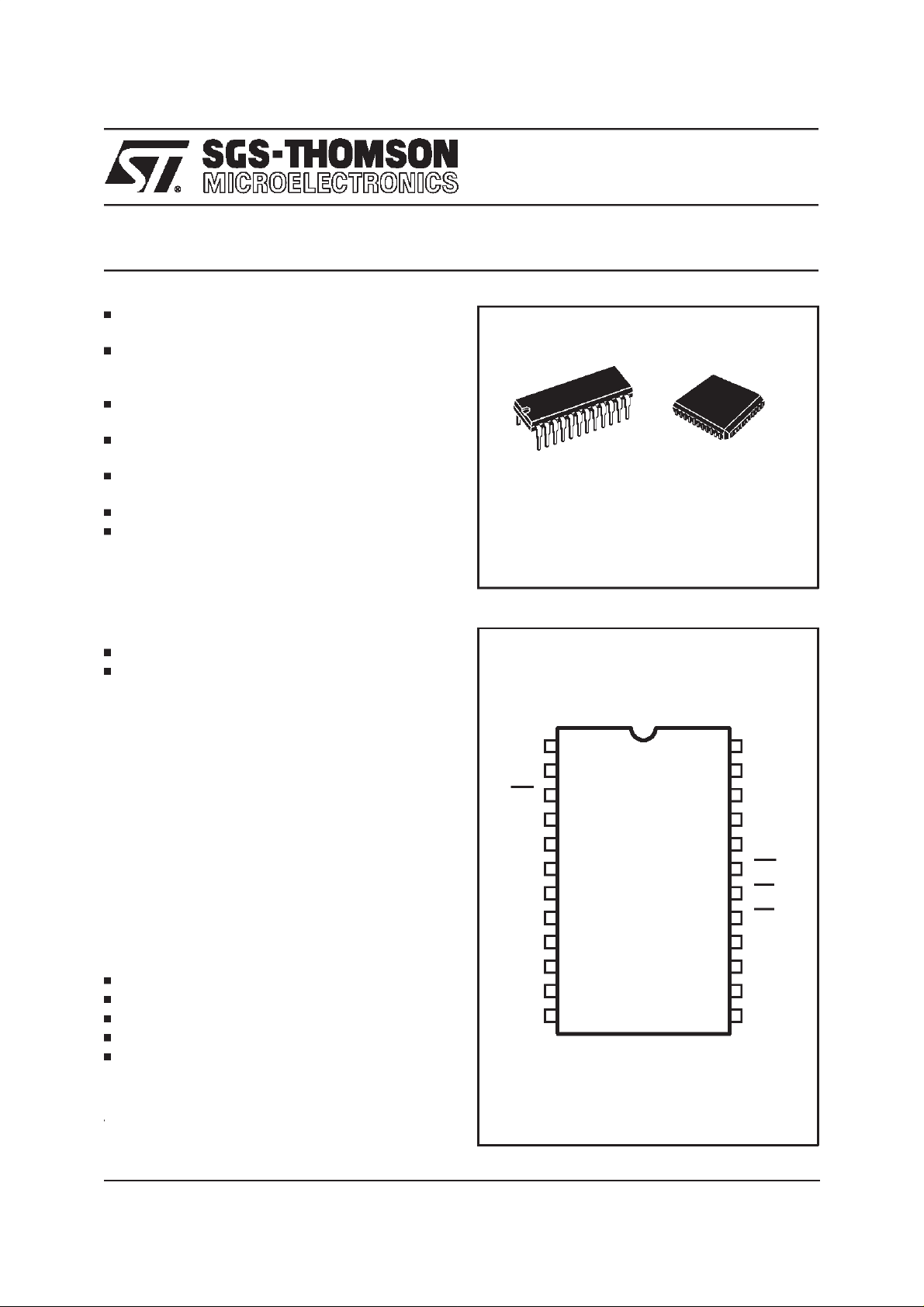
STLC5444
DIP24 PLCC44
ORDERING NUMBERS: STLC5444B1 (DIP24)
STLC5444FN (PLCC44)
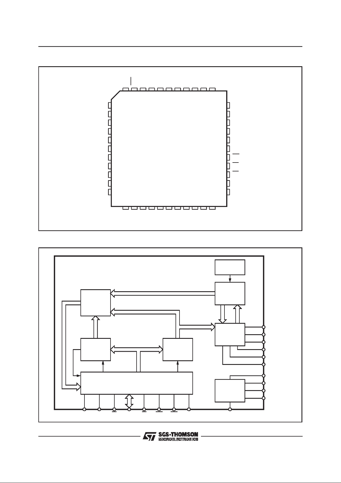
DIP24 PINCONNECTION (Top view)
DESCRIPTION
The ISDN Quad Feeder Power Supply (IQFPS)
provides a power source for up to four line interfaces. The power source to the device is a local
battery or a centralizedregulatedpower supply.
It can operate in point-to-point and point-to-multipoint configurations as far as S interface is concerned.
By the device microprocessor interface, each
powered line is individually controlled and monitored.
Therefore,overloads and faultsare easy to detect
and localizeeven in a large system.
The status conditions detected by the device on
each line that may be read by the microprocessor
are :
low output voltage
openloop
currentoverload
thermaloverload
normalline conditions
A hardware currentlimiting programmable feature
is available.
D1
D0
INT
BGND
VCC ALE
ILIM
N.C.
VBB
N.C.
S0
S1
VBB
1
2
3
4
5
6
7
8
9
10
11
12
D94TL102
24
23
22
21
20
18
17
16
15
14
13
D2
D3
A0
DGND
WR19
CS
RD
RESET
S3
RSRVD
S2
December 1997
1/17
Page 2
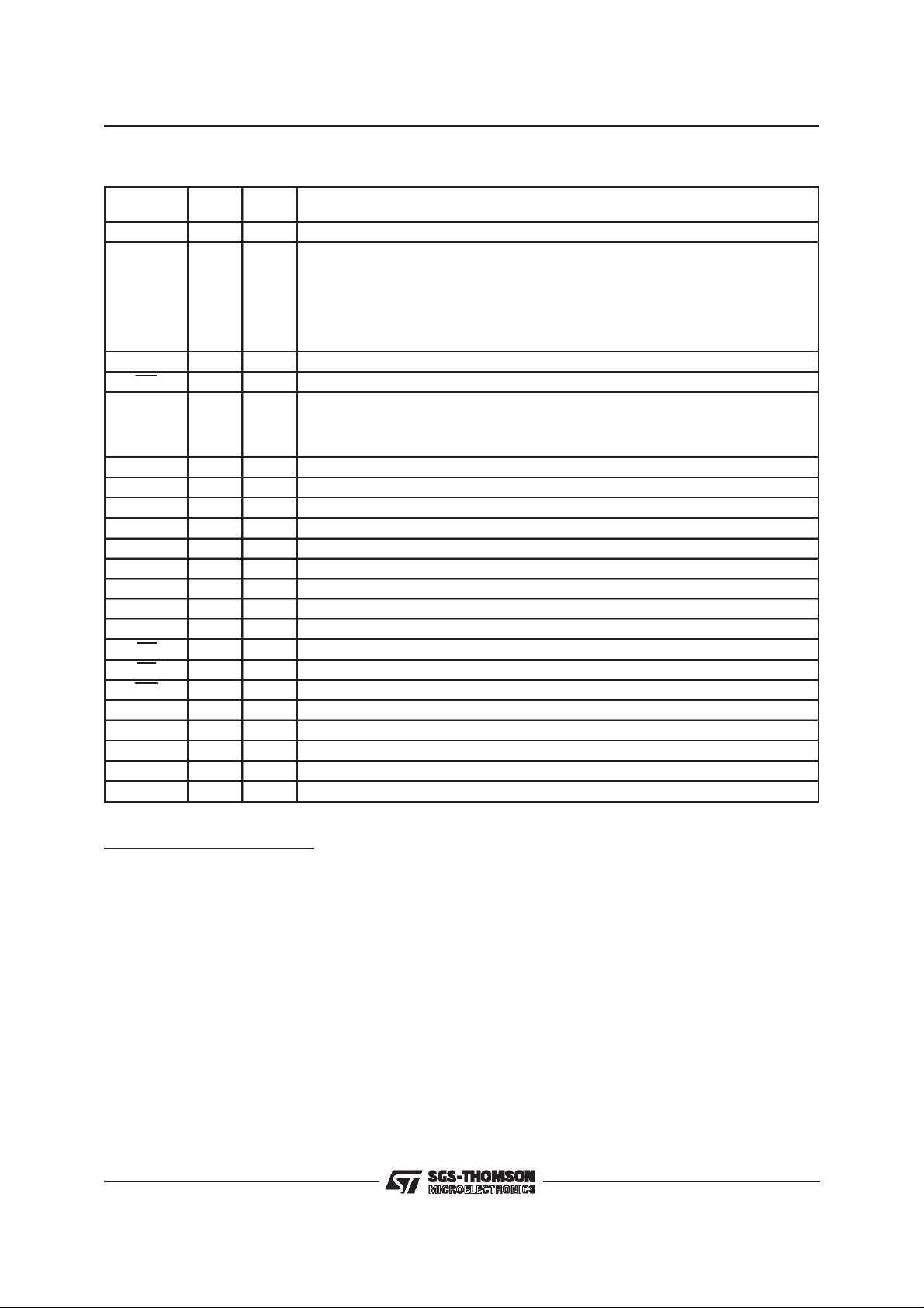
STLC5444
PLCC44 PIN CONNECTION (Top view)
VBB
INT
N.C.
D0
N.C.
D1
N.C.
D2
D3
A0
VBB
BLOCK DIAGRAM
VBB
N.C.
BGND
N.C.
VCC
ILIM
N.C.
N.C.
VBB
N.C.
VBB
7
8
9
10
11
12
13
14
15
16
17
N.C.
S0
N.C.
S1
123564
2322211918 20 28272624 25
N.C.
VBB
S2
N.C.
N.C.
S3
40414244 43
39
38
37
36
35
34
33
32
31
30
29
N.C.
VBB
N.C.
N.C.
DGND
ALE
N.C.
WR
CS
RD
RESET
VBB
D94TL103
2/17
BIT 3
OUTPUT
BUS D3/D0
THERMAL
OVERLOAD
STATUS GROUP BUS
MUX
ADDRESS
INDIRECT
ADDRESS
REGISTER
INT EN
ALE A0 CS D3/D0 RD WR INT RESET ILIM
LINE ENABLE REGISTER BUS
BUS 0/2
INPUT BUS D3/D0
IAR EN
µP
INTERFACE
S DRIVERS
DISABLE
O/3
LINE
ENABLE
REGISTER
LER EN
STATUS
DETECTOR
S
DRIVERS
VOLTAGE
REFERENCE
LINE
STATUS
BUS
S0
S1
S2
S3
VBB(12)
BGND
DGND
VCC
VBB(8)
D94TL104B
Page 3
PIN DESCRIPTION
o
Name
D1 1 1 Bit 1 of the tri state I/O data bus
NC 2,4,8,10,
D0 3 2 Bit 0 of the tri state I/O data bus
INT 5 3 Active low interrupt output for the µP (open drain)
VBB 6,7
BGND 9 4 Battery ground line
VCC 11 5 +5V supply line
ILIM 12 6 Current limit programming
S0 19 10 Output of the power switch controller 0
S1 21 11 Output of the power switch controller 1
S2 24 13 Output of the power switch controller 2
RSRVD – 14 Reserved pin:it must be left floating
S3 27 15 Output of the power switch controller 3
RESET 30 16 Active high reset input
RD 31 17 Active low read input
CS 32 18 Active low chip select input
WR 33 19 Active low write input
ALE 35 20 Active high address latch enable
DGND 36 21 Digital ground
A0 41 22 Address bit for R/W operations on the data bus
D3 42 23 Bit 3of the I/O tristate data bus
D2 43 24 Bit 2of the I/O tristate data bus
N
PLCC
13,14,
16,18,
20,23,
25,26,
28,34,
37,38,44
15,17
22,29,
39,40
o
N
DIP
7,9 No connection
8,12 Battery supply line (negative battery‘s terminal)
STLC5444
Function
FUNCTIONAL DESCRIPTION
ADDRESS LINE(Input)
A0 selects source and destination locations for
read and write operations on the data bus. A0
must be valid on the falling edge of ALE or during
RD and WR if ALE istied High.
ALE - Address Latch Enable (Input; Active
High)
ALE is an input control pulse used to strobe the
address on the A0 line into the address latch.
This signal is active High to admit the input address. The address is latched on the High-Low
transition of ALE. While ALE is High, the address
latch is transparent. For an unmultiplexed microprocessorbus, ALEmust be tiedHigh.
BGND - GroundBattery
CS - Chip Select(Input; Active Low)
CS must be Low to enable the read or write operations of the device. Data transfer occurs over
the D3-D0 lines.
D3-D0 - DATA BUS (Input/Output; Three-State)
The four bidirectional data bus lines are to exchange information with a microprocessor. D0 is
the least significant bit and D3 is the most significant bit. A High on the data bus corresponds to a
logical 1. These lines act as input when WR and
CS are active and as output when RD and CS are
active. When CS is inactive, the D3-D0 pins are
placed in a high-impedancestate.
3/17
Page 4

STLC5444
FUNCTIONAL DESCRIPTION (continued)
DGND - Ground Digital
ILIM - Current Limit Programming (Input)
ILIM programs the current limit of the Output drivers using an external resistor connectedbetween
ILIM and VBB. The ILIM pin is 1.25V more positive than VBB. The current limit is 5mA plus 1000
times the current in the external resistor.The programmed currentlimit applies to each driver.
INT - Interrupt (Output; Open-Collector, Active
Low)
INT augments the Microprocessor Interface by
generating an interrupt when a Current Overload
Detector (COD) occurs. INT is active whenever
any bits in the COD register are active. INT is not
latched; when the COD register is zero, INT goes
inactive (High). INT will also go inactive if the
IQFPS automatically disables the S-output driver
that caused the interrupt (due to Thermal Overload), or if the microprocessor disables that line
via the Line Enable Register (LER). COD interrupts can be masked via the Indirect Address
Register (IAR); RESET always disables the INT
pin.
transferredto D3-D0.
RESET- Reset (Input;Active High)
RESET initialize the registers in the device, leaving the driversswitchedoff.
S3-S0 - Drivers(Output)
S3-S0 each supplypower to one line. The outputs
can sink up to 120 mA each. The voltage at the
line is connected to VBBthrough a DMOSswitch.
VBB - BatteryVoltage (input)
VBB is the internal negative supply voltage. VBB
must always be connected to the most negative
supply voltage. The MPI Registers will not function properly when the battery power is disconnected, that is, when VBB is floating or grounded.
The IQFPS should also be reset if a drastic transientis applied to VBB.
VCC - +5VPower Supply(Input)
RD - Read (Input; Active Low)
The active Low read signal is conditioned by CS
and transfers internal information to the data bus.
If A0 is a logical 0, logic levels of the Indirect Address Register (IAR) and Thermal Shutdown
Status bit will be transferred to D3-D0. If A0 is a
logical 1, the data addressed by the IAR will be
WR - Write (Input; Active Low)
The active Low write signal is conditioned by CS
and transfers information from the data bus to an
internal register selected by A0. If A0 is a logical
1, D3-D0 is written into the Line Enable Register
(LER). If A0 is a logical 0, D3-D0 is written into
the IAR. LER and IAR are the only two writable
registersin thedevice.
4/17
Page 5
STLC5444
DC CHARACTERISTICS (VBB= -54V; VCC= 5V;unlessotherwise specified)
Symbol Parameter Test Conditions Min. Typ. Max. Unit
Input Voltage High Level 2 V
IH
Input Voltage Low Level 0.8 V
IL
High Level Output Current VOH= 2.4V 400 µA
Low Level Output Current VOL= 0.4V 2 mA
High Level Input Current VIH=2V 10 µA
IH
Low Level Input Current VIL= 0.8V 60 µA
IL
Output Hi-Z Current High 2.4V < VOZ<V
CC
Output Hi-Z Current Low 0V < VOZ< 0.4V 10 µA
VCCsupply Current 1.4 5 mA
Logic I/OCapacitance 10 pF
L
Saturation Voltage IS= 80mA 2 V
Output DMOS Saturation Resistivity IS= 80mA 25
on
VBBSupply Current VBB= -54V, R
= 26.6KΩ,
LIM
3.2 6 mA
10 µA
Ω
V
V
V
I
I
I
I
I
OZH
I
OZL
I
C
R
I
OH
OL
CC
SAT
BB
Output Disabled
I
∆
SLIM
Delta Limit Current vs.
Theoretical Programmed Value
I
SLIM
R
= 26.6KΩ,VBB= -96V
LIM
R
= 10.9KΩ,VBB= -54V
LIM
10%
±
V
I
SOL
LVD
Low Voltage Detector Threshold
(relative to V
BB
)
Current Overload Detector
Threshold (as % of I
I
SOC
I
Open Loop Detector Threshold 1.5 3 4 mA
Si Leakage Current to ground @
SZ
Si disabled
H
H
H
LVD
OLD
COD
Low Voltage Detector Hysteresis 18 200 mV
Open Loop Detector Hysteresis 0.6 1.6 mA
Current Overload Detector
Hysteresis
H1 130°C Thermal Detector
Hysteresis
H2 160°C Thermal Detector
Hysteresis
T
Thermal Overload Recovery
H1
Time H1
SLIM
S3 - S0 output active 2.7 3 3.3 V
75 90 %
)
VBB= -110V 100
A
µ
2.4 4.0 mA
10
C
°
10 °C
80 µs
5/17
Page 6
STLC5444
SWITCHINGCHARACTERISTICS (VBB= -54V;VCC=5V; unlessotherwisespecified)
MICROPROCESSOR READ/WRITE TIMING NON MULTIPLEXEDMODE (for references see figure 1a
and 2b).
Symbol Parameter Min. Max. Unit
t
RLRH
t
RHRL
t
RLDA
t
RHDZ
t
ASRL
t
AHRH
t
ASWL
t
AHWH
t
ADDA
t
WLWH
t
WHWL
t
DAWH
t
WHDZ
t
RES
Note: AC timingsare tested at 0.8V and 2V with input levelsof 0.4V and 2.4V.
RD, CS pulse width 260 ns
RD, recovery time T
T
: -40 to 0°C and +70°C to +85°C
amb
: 0 to 70°C
amb
200
220
ns
ns
RD, CS low to data available 260 ns
RD or CS high to data Z T
T
: -40 to 0°C and +70°C to +85°C
amb
: 0 to 70°C
amb
130
160
ns
ns
Address setup time to READ active 0 ns
Address hold time to READ inactive 0 ns
Address setup time to WRITE active 30 ns
Addess hold time to WRITE inactive 50 ns
Address stable to data available T
T
: -40 to 0°C and +70°C to +85°C
amb
: 0 to 70°C
amb
360
390
ns
ns
WR or CS pulse width 200 ns
Write recovery time 200 ns
Data setup time 100 ns
Data hold time T
T
: -40 to 0°C and +70°C to +85°C
amb
: 0 to 70°C
amb
20
40
ns
ns
Reset Pulse with 200 ns
SWITCHINGCHARACTERISTICS (V
= -54V;VCC=5V; unlessotherwisespecified)
BB
MICROPROCESSORREAD/WRITE TIMINGMULTIPLEXEDMODE (for references see figure1 and 2).
Symbol Parameter Min. Max. Unit
t
RLRH
t
RHRL
t
RLDA
t
RHDZ
t
AHAL
t
ADAL
t
ADAZ
t
AZRL
t
AZWL
t
ADDA
t
WLWH
t
WHWL
t
DAWH
t
WHDZ
t
RES
RD, CS pulse width 260 ns
RD, recovery time T
T
: -40 to 0°C and +70°C to +85°C
amb
: 0 to 70°C
amb
200
220
ns
ns
RD, CS low to data available 260 ns
RD or CS high to data Z T
T
: -40 to 0°C and +70°C to +85°C
amb
: 0 to 70°C
amb
130
160
ns
ns
ALE pulse width 100 ns
Address setup time 60 ns
Address hold time 50 ns
Address Z to RD low 0 ns
Address Z to WR Low 0 ns
Address stable to data available T
T
: -40 to 0°C and +70°C to +85°C
amb
: 0 to 70°C
amb
360
390
ns
ns
WR or CS pulse width 200 ns
Write recovery time 200 ns
Data setup time 100 ns
Data hold time T
T
: -40 to 0°C and +70°C to +85°C
amb
: 0 to 70°C
amb
20
40
ns
ns
Reset Pulse with 200 ns
Note: AC timingsare tested at 0.8V and 2V with input levelsof 0.4V and 2.4V.
Si Timing (at10% offinalvalue)
Symbol Parameter Test condition Typ. Max. Unit
t
EN
t
DIS
Si output enable time (from LER) R
Si output disable time (from LER or RESET) 3 6 µs
=3kΩ 25µs
LOAD
6/17
Page 7

Figure 1: MicroprocessorRead Timing.
t
ALE
A
CS
RD
O
AHAL
t
ADALtADAZ
t
ADDA
t
t
AZRL
CLRL
(Note 1)
t
RLDA
t
RLRH
t
Read DataDATA
RHCH
(Note 2)
t
RHDZ
t
RHRL
STLC5444
D94TL108A
Notes:
1 - Ift
2 - Ift
is negative,t
CLRL
is negative,t
RHCH
RHRL,tRLRH,tAZRL
RHRL,tRLRH
and t
, andt
RHDZ
aremeasured from CS rather than RD.
RLDA
aremeasured from CS rather than RD.
When a read from the LER immediately follows a write to the LER a minimum of 1 µs is required between these operations.
Figure 2: MicroprocessorWrite Timing.
t
ALE
A
CS
WR
INT
O
AHAL
t
ADALtADAZ
t
CLWL
(Note 1)
t
AZWL
t
WLWH
t
DAWH
Write DataDATA
t
WHCH
t
WHDZ
(Note 2)
(Note 3)
t
WHWL
D94TL109A
Notes:
1 - Ift
2 - Ift
CLWL
WHCH
is negativet
isnegative, t
and t
WHWL
WHWL,tWLWH,tDAWH
WLWH
aremeasured from CS rather than WR.
and t
are measured from CS rather than WR.
WHDZ
The propagationdelay from the writing of the T/I bit tothe effect on the INT pin is approximately 1µs for both mask and enable operations.
7/17
Page 8

STLC5444
Figure 1a: MicroprocessorRead Timing non multiplexed mode.
ALE
A
O
t
AHRH
t
CLRL
(Note 1)
t
RHCH
(Note 2)
CS
t
RD
t
ADDA
ASRL
t
RLDA
t
RLRH
t
RHDZ
Read DataDATA
t
RHRL
D97TL301A
Notes:
1 - Ift
2 - Ift
is negative,t
CLRL
is negative,t
RHCH
RHRL,tRLRH,tAZRL
RHRL,tRLRH
and t
, andt
RHDZ
aremeasured from CS rather than RD.
RLDA
aremeasured from CS rather than RD.
When a read from the LER immediately follows a write to the LER a minimum of 1 µs is required between these operations.
Figure 2a: MicroprocessorWrite Timing non multiplexed mode.
ALE
t
ASWL
A
O
t
AHWH
t
(Note 2)
CS
WR
t
CLWL
(Note 1)
t
WLWH
t
DAWH
Write DataDATA
WHCH
t
WHDZ
(Note 3)
t
WHWL
INT
D97TL302A
Notes:
1 - Ift
2 - Ift
CLWL
WHCH
is negativet
isnegative, t
and t
WHWL
WHWL,tWLWH,tDAWH
WLWH
aremeasured from CS rather than WR.
and t
are measured from CS rather than WR.
WHDZ
The propagationdelay from the writing of the T/I bit tothe effect on the INT pin is approximately 1µs for both mask and enable operations.
8/17
Page 9

STLC5444
OPERATIVEDESCRIPTION.
Initialization
The device is initialized by the RESET pin. In this
state the analog drivers are switched off, the Indirect Address Register(IAR) is cleared,and the internally latchedaddress A0 is cleared.
Power at Outputdrivers
The voltage at the Outputdrivers is approximately
V
(moreprecisely: VBB-V
BB
SAT
).
Analog Section
The analog section consists of four line drivers,
which are DMOS transistor switches capable of
sinking up to 120 mA each. Thepower to the drivers is derived from the negative supply voltage
). The output voltage to each line is slaved to
(V
BB
V
, and the voltage drop in each driver is ap-
BB
proximately1.5V.
Line driver protection is provided through the inte-
gration of currentlimit and over-temperatureshutoff. The current limit is hardware-programmable
via an external resistor (RLIM) connected between ILIM and V
BB
.
The output limit is : 5mA + 1000 x 1.25V/RLIM.
This 1000 x gain makes the ILIM pin susceptible
to externalnoise, care should be taken toconnect
RLIM as close as possible to the component.
The thermal shut-off is internally set at approximately 160
o
C.
At this temperature all the driversare unconditionally switched off. However, at approximately
o
130
C, only the drivers that are in the current-
overload conditionwill be turnedoff.
Status detectors, associated with each of the line
drivers, monitor the load conditions on each line
by comparing an electrical parameter (e.g., current and voltage at the line) with reference level.
The output of each detector can be read by the
microprocessor.In addition to these status detectors, the temperature of the device is monitored
via integrated temperature detectors. The detectors respond at approximately 130
as defined above, and the 160
o
C and 160oC,
o
C detector can be
monitoredby the microprocessorvia the MPI. The
status detectorsprovide the following information
from each of the lines (all detectors have built-in
hysteresis):
*) Low OutputVoltage Detection
The low-output-voltagestatus bit becomesactive whenthe voltage across the output DMOS
transistorexceeds the proper voltage threshold
).
(V
LVD
*) OpenLoop Detection
Theopen-loop statusbit becomesactive when
the currenton the linedropsbelowa minimum
value.
*) CurrentOverload Detection
Thecurrent-overloadstatus bitsbecome active
when the currenton the linenears the current
limit. Thesebits active the INT outputif COD interruptsare enabledvia the IARRegister.
*) ThermalOverload Detection
If the devicetemperaturereaches 130
o
C, then
all the line driversin the current-overloadconditionwill be switchedoff and the corresponding
bitsin the Thermal OverloadRegister will be
activated.If the device temperatureincreases
o
to 160
C, all the line drivers will be turned off,
and all the bits in the Thermal OverloadRegister will be activated.
TheT-bit will also be set, and it can be read
alongwith the IndirectAddressRegister(IAR)
to indicatethat all the drivershave beenturned
off. To initializeany of the bits in the Thermal
OverloadRegister, the microprocessormust
firstturn off the line driversthat must notbe reactivateduntil the T-bit in the address register
is clearedby the temperaturedetector in the
device.
MPI Section
The MPI allows the user to access the detectors
defined in the analog section. The line driver’s
status bitsare grouped by function.Bits 3-0 of the
detectorscorrespondto lines 3-0, respectively.
The statusgroup are :
Low VoltageDetector (LVD)
Open Loop Detector(OLD)
CurrentOverload Detector (COD)
ThermalOverload Register (TOR)
The data is not latched in these status groups except in the TOR.
Thus, the user should filter (multiple samples) the
received data to ensure its integrity. There are
two other registers in the MPI: the Indirect Address Register (IAR), and Line Enable Register
(LER).
The IAR contains 3 bits that address the desired
status group or the LER. The IAR is read along
with the T-bit defined in the analog section. The
microprocessorcan read the IAR to check the validity of the address. A 1us delay is required between a write to the LER register, followed by a
Read of the same register. Subsequent reads of
the LER do not have this constraint.
9/17
Page 10

STLC5444
The LER is used to enable or disable the individual line drivers. The line drivers will only become
active if the corresponding bit in the TOR is inactive. The LER is a read/writeregister.
The MPI is the interface containing the following
pins :
D3-D0 Bidirectional DataBus
A0 Input Address Line
ALE Input Address Latch Enable
RD Input ReadEnable
WR Input Write Enable
CS Input Chip Select
INT Output COD Interrupt
RESET Input Reset pin
The 4-bit bidirectionaldata bus (D3-D0) is used to
communicate with the registers. Access to the
registers is controlled by CS, RD, WR, ALE, and
A0 as shown below. Aread or write cyclemust be
preceded by a valid A0. A0 is latched internally in
a transparent latch by ALE. The selection of the
status groupor the LER is determinedby the content of the IAR.
The truth table for the MPI control is shownbelow
:
CS RD WR A0
0 1 0 0 WriteIAR (T bitis read only)
0 0 1 0 Read IAR and T bit
0 1 0 1 WriteLER
0 0 1 1 Read status groups or LER
1 X X X No access
Indirect Address Register(IAR) and T/I Bit
The IAR is 3 bits wide and accessiblethroughthe
data port, D2-D0. The content of the Indirect Address Register (IAR2-IARO) determines the selection of the status groups or the LER. The thermal overload bit T/I is read and written at the
sametime as IAR and occupies D3.
This registerhas the followingformat :
Bit Symbol
0
1
2
3
IARO
IAR1
IAR2
T/I
Bit 0 of the IAR
Bit 1 of the IAR
Bit 2 of the IAR
T bit: (Read only)
Logical 0: temperature normal (default value)
Logical 1: temperature above 160°C (all driversshut off)
I bit : (write only)
Logical 0: INT pin disabled
Logical 1: COD interrupts enabled via INT pin‘
IAR2-IAR0 addressthe status groups and the LER as shownbelow:
IAR2 IAR1 IAR0 Select
0
0
0
0
1
1
1
1
0
0
1
1
0
0
1
1
0
1
0
1
0
1
0
1
LVD
OLD
COD
LEC
RESERVED
RESERVED
LER
TOR
10/17
Page 11

STLC5444
The contentsand format of the statusgroups andthe LER are as follows :
LVD:
Bit Logical 1 Logical 0 (default value)
0
1
2
3
O0 low voltage
O1 low voltage
O2 low voltage
O3 low voltage
The Low Voltage Detector (LVD) indicates the voltage level on the output lines, even when the lines are
disabled. The low-voltage condition becomes active (logical 1) if the output reaches the Low Voltage
Threshold(VLVD).
LEC:
Bit Logical 1 Logical 0
0
1
2
3
SWITCH ON
SWITCH ON
SWITCH ON
SWITCH ON
The Line Enable Command(LEC) indicates the statusof the DMOS SWITCHOUTPUT.
OLD:
Bit Logical 1 Logical 0 (default value)
0
1
2
3
O0 open loop
O1 open loop
O2 open loop
O3 open loop
O0 voltage normal
O1 voltage normal
O2 voltage normal
O3 voltage normal
SWITCH OFF
SWITCH OFF
SWITCH OFF
SWITCH OFF
O0 current normal
O1 current normal
O2 current normal
O3 current normal
The Open Loop Detector (OLD) indicates the open-loop condition on the output lines. The open-loop
conditionbecomes active (logical1) if the currenton the line dropsbelowthe thresholdvalue ISOC.
COD:
Bit Logical 1 Logical 0 (default value)
0
1
2
3
O0 current overload
O1 current overload
O2 current overload
O3 current overload
O0 current normal
O1 current normal
O2 current normal
O3 current normal
The Current Overload Detector (COD) indicates the current-overloadcondition on the output lines. The
overload condition becomes active (logical 1) if the output current approaches the value programmed by
an externalresistor betweenILIM and VBB.
TOR:
Bit Logical 1 (default value) Logical 0
0
1
2
3
The Thermal Overload Register (TOR) contains the overload status of the output line drivers. If the device temperature reaches 130
o
C, then the output line drivers that are in the current-overload condition
O0 operational
O1 operational
O2 operational
O3 operational
O0 off
O1 off
O2 off
O3 off
will be switched off. The corresponding bits in the TOR will be set to a logical 0. To initialize any of the
bits in the TOR, the microprocessor must first turn off the output line drivers via the LER. However, the
TOR bits cannot be deactivated if the 160
o
C detectoris active.The µp may re-enable the output drivers
via the LER after the TOR condition is removed.The TOR is a read-onlyregister.
11/17
Page 12

STLC5444
LER:
Bit Logical 1 Logical 0 (default value)
0
1
2
3
O0 on
O1 on
O2 on
O3 on
The Line Enable Register (LER) is usedto enable or disable the individual outputline drivers.The output
line will only become active if the correspondingbit in the TOR is set to a logical 1. The LER can be written directlyand read indirectly.
O0 off
O1 off
O2 off
O3 off
ABSOLUTE MAXIMUM RATINGS (T
Parameter Value
Voltage from Digital Input to DGND -0.4V to V
Voltage from VCCto DGND -0.4Vto +7V
Voltage from V
100ns Pulse voltage from Si to DGND (See Notes) -130V to +2V
Voltage from BGND to DGND +0.5V, -3V
Storage Temperature T = -60°C to +150°C
Note : Si stands for O0, O1, O2 or O3 outputs.
to DGND -130V to +0.4V
BB
=0°Cto70°C)
A
CC
RECOMMENDED OPERATINGCONDITIONS
Parameter Symbol1 Min. Max. Units
(*) Ambient Temperature for standard type
Supply Voltage V
Programmed Limiting Current I
Note: The test conditionis specified with a diode in series withVBB.
(*): Specificationsin this data sheet are guaranteed by testing from 0°C to +70°C. For extended temperature range types, performance from
–40°C to +85°C is guaranteed by characterization and periodic sampling of production units.
for ext. temperature type
T
A
T
A
CC
V
BB
DGND
BGND
SLIM
0
-40
4.75
-115
0
-3
70
85
5.25
-38
0
+0.5
120 mA
°C
°
C
V
V
V
V
ORDERINGTYPES:
STLC5444B1,PDIP24 package:0 to 70°CTemperature range.
STLC5444FN,PLCC44 package: 0 to 70°C Temperaturerange.
STLC5444B1-X,PDIP24 package:-40 to 85°C Temperaturerange.
STLC5444FN-X,PLCC44 package:-40 to 85°CTemperaturerange.
APPLICATIONHINT
In the Absolute MaximumRatings table it is specified that the voltage applied on the -V
bat
pin
should never exceed by more than 0.4V the voltage applied on the Groundpin.
As long as the external circuitry assures compliance with the above, no more considerationsare
needed.
In some cases however it may be not possible to
exclude that conditions may occur (hot insertion,
power supply transients, etc.) where the negative
supply has a transient overshoot above ground
voltage. Then a protection circuitry that clamps
such overshootcan add to the equipment reliability. Such protection can be designed taking into
considerations that typically the devices behave
as follows:
12/17
- if the V
pin is not connected,and the other
bat
pins are normally biased, the chip generates
on it an open circuit voltageof +420mV.
- if all the other pins are normally biased and
the -V
pin forced at +600mV, a current of
bat
10mAflows into it. At the same time from +5V
a current of 4mA is absorbed (this low current
from +5V simply means that no parasitic
latch-ups are triggered inside the chip). No
deteriorationof the device occurs.
- if all the other pins are normally biased, and
the -V
pin is forced at +1.5V for a transient
bat
period, no deterioration of the device occurs.
Transient period can be considered any time
intervalthat lasts for less than 10µs and is not
repeated more than 5000 times during the
devicelifetime.
Page 13

COUNTERFEEDING
It is possible that, in some applications,a communication channel that the STLC5444 feeds, is also
biased at the other end by another feeding device.
Figure 3: Typical PABXconnection.
U
STLC5444
What considerations apply to the STLC5444 in
this case?
Let’susea genericexampleforreference(seeFig. 3)
S
S
STLC5444
V
D95TL229
A PABX with S-interfaces may have some of
Si
BB
3) In the channel of the STLC5444 on the PABX
them connectedto TerminalEquipments, and one
to the S-interface of a Nertwork Termination. The
S-interface of the PABX connected to the NT has
one channel of the STLC5444 available for feeding. It will be programmed in the ”OFF” state to
avoid interference with the feeding coming from
the NT (of course the feeding coming from the NT
4) It is good common practice to provide every Swill not be loaded by thisPABX connection).
The following considerations are relevant in the
above example:
1) The VBB of the STLC5444 in the PABX must
be equal or more negative than the feeding
voltage coming from the NT (unless decouplingdiodes are externallyprovided- see 4)
2) The STLC5444 channel of the PABX must be
programmedOFF.
Figure 4: Protectionof the STLC5444against overvoltage.
Si
STLC5444
V
BB
PABXNT
S
side, the only effect will be on the relevant
LVD bit that will be set to 1 if the feeding voltage coming from the NT is 3V more positive
than the local VBB. No interrupts or alarmsare
generated.
interface with protection circuitry against transient overvoltages(see Fig. 4). This includes a
diode in series with each Si pin of the
STLC5444. If this is the case, absolute levels
of local VBB and NT feeding are no concernat
all. (If such diodes are not present, care must
be paid to the power supply of the PABX, and
to the connected circuits. When the PABX
supply is OFF, the NT feeding will find a connection through the relevant channel of the
STLC5444tothe VBBpoint).
BGND
BGND
STLC5444
V
BB
BATTERY
D2
D1
TPAXX
D3
Si
D95TL230
FUSE RESISTORS S INTERFACE
13/17
Page 14

STLC5444
NOTE
Possible effect on the device of a Vbat variation
Be aware that a variation of Vbat during operation, when the switches are on can cause anomalous behaviour. To avoid that a turn-off occurs the variation should have a rise time equal or lower than
20V/µs (fig. 5), and a fall time equal or lower than 2.0V/µs (fig.6).
Figure 5: Typical rise timebehaviour.
Vbat1
Fail dV/dt > 25V/µs
OK dV/dt < 20V/µs
Vbat0
D97TL303
Figure6: Typicalfall time behaviour.
D97TL304
Vbat1
OK dV/dt < 2.0V/µs
Fail dV/dt > 2.4V/µs
Vbat0
14/17
Page 15

DIP24 PACKAGEMECHANICAL DATA
STLC5444
DIM.
MIN. TYP. MAX. MIN. TYP. MAX.
a1 0.63 0.025
b 0.45 0.018
b1 0.23 0.31 0.009 0.012
b2 1.27 0.050
D 32.2 1.268
E 15.2 16.68 0.598 0.657
e 2.54 0.100
e3 27.94 1.100
F 14.1 0.555
I 4.445 0.175
L 3.3 0.130
mm inch
15/17
Page 16

STLC5444
PLCC44 PACKAGEMECHANICALDATA
DIM.
MIN. TYP. MAX. MIN. TYP. MAX.
A 17.4 17.65 0.685 0.695
B 16.51 16.65 0.650 0.656
C 3.65 3.7 0.144 0.146
D 4.2 4.57 0.165 0.180
d1 2.59 2.74 0.102 0.108
d2 0.68 0.027
E 14.99 16 0.590 0.630
e 1.27 0.050
e3 12.7 0.500
F 0.46 0.018
F1 0.71 0.028
G 0.101 0.004
M 1.16 0.046
M1 1.14 0.045
mm inch
16/17
Page 17

STLC5444
ESD- The SGS-THOMSON Internal Quality Standards set a target of 2 KV that each pin of the device should withstand in a series of tests
based on theHuman Body Model (MIL-STD 883 Method 3015): with C = 100pF; R = 1500Ω and performing 3 pulses for each pin versus V
and GND.
Device characterization showed that, in front of the SGS-THOMSON Internaly Quality Standards, all pins of STLC5444 withstand at least
1000V.
The above points are not expected to represent a pratical limit for the correct device utilization nor for its reliability in the field. Nonetheless
they must bementionned in connection with the applicabilityof the different SURE 6 requirements to STLC5444.
Information furnished is believed to be accurate and reliable. However, SGS-THOMSON Microelectronics assumes no responsibility for the
consequences of use of such information nor for any infringement of patents or other rights of third partieswhich may result from its use. No
license is granted by implication or otherwise under any patent or patent rights of SGS-THOMSON Microelectronics. Specificationmentioned
in this publication are subject to change without notice. This publication supersedes and replaces all information previously supplied. SGSTHOMSON Microelectronics products are not authorized for use as critical components in life support devices or systems without express
written approval of SGS-THOMSON Microelectronics.
1997SGS-THOMSON Microelectronics – Printedin Italy – All Rights Reserved
SGS-THOMSON Microelectronics GROUP OF COMPANIES
Australia - Brazil - Canada - China- France - Germany - Italy - Japan - Korea - Malaysia -Malta - Morocco - The Netherlands-
Singapore - Spain - Sweden - Switzerland- Taiwan - Thailand -United Kingdom- U.S.A.
17/17
CC
 Loading...