

Page 1
GENERAL FEATURES
SINGLECHIP2B1QLINECODETRANSCEIVER
SUITABLEFOR ISDN, PAIR GAIN AND DECT
APPLICATIONS
MEETS OR EXCE ED S ETSI EUROPEAN
STANDARD
SINGLE5V SUPPLY
DIP28 AND PLCC44 PACKAGE
HCMOS3A SGS-THOMSON ADVANCED
1.2µm DOUBLE-METALCMOS PROCESS
ROUND TRIPDELAY MEASUREMENT
EXTENDED TEMPERATURE RANGE (-40°C
TO +70°C)
TRANSMISSIONFEATURES
160 KBIT/S FULL DUPLEX TRANSCEIVER
2B1Q LINE CODING WITH SCRAMBLER/DE-
SCRAMBLER
SUPPORTS BRIDGE TAPS, SPLICES AND
MIXED GAUGES
>70DBADAPTIVEECHO-CANCELLATION
ON CHIP HYBRID CIRCUIT
DECISIONFEEDBACKEQUALIZATION
ON CHIP ANALOG VCO SYSTEM
DIRECT CONNECTION TO SMALL LINE
TRANSFORMER
STLC5412
2B1Q U INTERFACEDEVICE
ENHANCED WITH DECT MODE
PRELIMINARY DATA
PLCC44
ORDERING NUMBER: STLC5412FN
Plastic DIP28
ORDERING NUMBER: STLC5412P
SYSTEM FEATURES
ACTIVATION/DEACTIVATIONCONTROLLER
ON CHIP CRC CALCULATION AND VERIFI-
CATION INCLUDING TWO PROGRAMMABLE BLOCKERROR COUNTERS
EOC CHANNEL AND OVERHEAD-BITS
TRANSMISSION WITH AUTOMATIC MESSAGE CHECKING
GCI AND µW/DSI MODULE INTERFACES
COMPATIBLE
DIGITAL LOOPBACKS
COMPLETE(2B+D)ANALOGLOOPBACKIN LT
ELASTIC DATA BUFFERS AND BACKPLANE
CLOCK DE-JITTERIZER
AUTOMODENT1 AND REPEATER
”U ACTIVATION ONLY”IN NT1
February 1999
This is preliminary information on a new product now in development or undergoingevaluation. Details are subject to change without notice.
IDENTIFICATIONCO DEAS PERGCISTANDARD
DECTFRAME SYNCHRONIZATION
EASILY INTERFACEABLE WITH ST5451
(HDLC & GCI CONTROLLER), STLC5464 /
STLC5465 AND ANY OTHER GCI, IDL or
TDM COMPATIBLEDEVICES
1/74
Page 2

STLC5412
INDEX
DISTINCTIVE CHARACTERISTICS .......................................... Page 1
GENERAL DESCRIPTION....................................................... 5
PIN FUNCTION .................................................. .............. 6
FUNCTIONAL DESCRIPTION............................................. ....... 14
Digital Interfaces. . . . .....................................................
µW/DSI mode . . . . . . ....................................... ..............
µ
W Control Interface. . . . .................................... ..............
WriteCycle . . . . . . . . . . . . . . . . . . . . ........................ ..........
ReadCycle............................................. ............1414
Digital SystemInterface. . .................................................
GCI mode. . . . . . . .....................................................1518
Frame structure. . . . . . . . ...........................................
Physicallinks . . . . . . . . . ............................................
Monitor channel. . . . . . . . . . . . . . .....................................
C/I channel.. . . ...................................................
Line coding and frameformat . . . ...........................................
Transmitsection. . . . . . . . .................................................
Receivesection..........................................................
Elasticbuffers............................................................
Dectsynchronization.......................................................
Maintenancefunctions. . . . . ............................................... 26
M channel.. .....................................................
EOC.............................................................
M4channel.......................................................
SpareM5andM6bits...............................................
CRC calculation checking. . . . . . . . . . . . . . . . . . . ........................
Loopbacks. . . . . . . . . . . . . . . . . . . . . . . . . . . . . . . . . . . . . . . . . . . . . . . . . . . . ..
Identificationcode. . .....................................................
GeneralpurposeI/Os......................................................
Testfunctions.. . .........................................................
14
14
14
18
18
22
23
23
24
24
25
25
26
27
27
27
27
27
34
34
35
Turningonandoffthedevice................................................
Power on initialization . . . . . . . ......................................
Line signaldetection . ............................................
Power up control . . . . . ....................................... ....
Power down control. . . . . . . .......................................
Power up state . ........................................... ......
Power down state . . . . . . . . . . . . . . ...................................
Activationdeactivationsequencing.. . . . . . . . . . . . . . . . . . . . . . . . . . . . . . . ...........
Case of restricted activation. . . . . . . . . . . . ...................................
Resetof activation / deactivationstate machine. .................................
Hardwarereset...........................................................
Quietmode..............................................................
Automode...............................................................
35
35
35
35
36
36
36
36
36
36
36
36
37
Command/Indication(C/I) codes. . ..........................................
Internalregisterdescription. . . .. . . . .............. ..........................3741
Line interface circuit . . ...................................................
Boardlayout . . .........................................................5555
APPENDIX A: STATEMATRIX................................................... 60
APPENDIX B: ELECTRICAL PARAMETERS ........................................ 62
2/74
Page 3
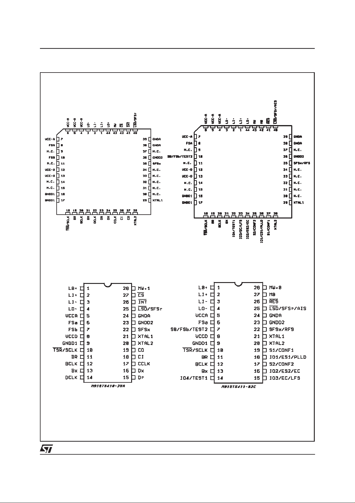
PIN CONNECTIONS (Topview)
STLC5412
PLCC44
MICROWIRE MODE
PLCC44
GCI MODE
DIP28
MICROWIRE MODE
DIP28
GCI MODE
3/74
Page 4
STLC5412
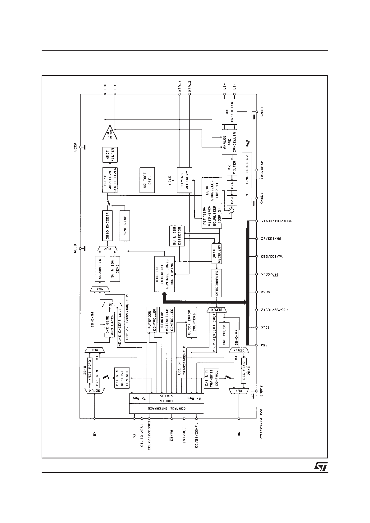
Figure 1: BlockDiagram.
4/74
Page 5

STLC5412
GENERAL DESCRIPTION
STLC5412 is a complete monolithic transceiver
for ISDN Basic access data transmission on
twisted pair subscriber loops typical of public
switched telephone networks. The device is fully
compatible with ETSI ETRO80 and CSE (C32-11)
French specifications.
The equivalent of 160 kbit/s full-duplex transmission on a single twisted pair is provided, according to the formats defined in the a.m. spec.
Frames include two B channels, each of 64 kbit/s,
one D channel of 16 kbit/s plus an additional 4
kbit/s M channel for loop maintenance and other
user functions. 12 kbit/s bandwidth is reserved for
framing. 2B1Q Line coding is used, where pairs of
bits are coded into one of 4 quantumlevels. This
technique results in a low frequency spectrum
(160 kbit/s turn into 80 kbaud), thereby reducing
both line attenuation and crosstalk and achieving
long rangewith low Bit Error Rates.
STLC5412 is designed to operate with Bit Error
Rate near-end Crosstalk (NEXT) as specified in
european ETSI recommendation.
To meet these very demanding specifications, the
device includes two Digital Signal Processors,
one configured as an adaptive Echo-Canceller to
cancel the near end echoes resulting from the
transmit/receive hybrid interface, the other as an
adaptive line equalizer. A Digital Phase-Locked
Loop (DPLL) timing recovery circuit is also included that provides in NT modes a 15.36 MHz
synchronized clock to the system. Scrambling
and descrambling are performed as specified in
the specifications.
On the system side, STLC5412 can be linked to
two bus configurationsimply by pin MWbias.
MICROWIRE(µW/DSI) mode (MWpin = 5V): 144
kbit/s 2B+D basic access data is transferredon a
multiplex Digital System Interface with 4 different
interface formats (see fig. 2 and 3) providing
maximum flexibility with a limited pin count
(BCLK, Bx, Br, FSa, FSb). Three pre-defined
2B+D formats plus an internal time slot assigner
allows direct connection of the UID to the most
common multiplexed digital interfaces (TDM/IDL).
Bit and Frame Synchronisationsignals are inputs
or outputs depending on the configuration selected. Data buffers allow any phase between the
line and the digital interface. That permits building
of slave-slave configurations e.g. in NT12 trunkcards.
It is possible to separate the D from the B chan-
nels and to transfer it on a separate digital interface (Dx, Dr) using the same bit and frame clocks
as for the B channelsor in a continuousmode using an internallygenerated16 kHz bit clockoutput
(DCLK).
All the Control, Status and Interrupt registers are
handledvia a control channel on a separate serial
interface MICROWIRE compatible (CI, CO, CS,
CCLK, INT) supported by a number of microcontroller including the MCU families from SGSTHOMSON
GCI mode (MWpin = 0V). Control/maintenance
channels are multiplexed with 2B+D basic access
data in a GCI compatible interfaceformat(see fig.
4a) requiring only 4 pins (BCLK, Bx, Br, FSa). On
chip GCI channel assignement allows to multiplex
on the same bus up to 8 GCI channels,each supporting data and controls of one device. Bit and
Frame Synchronisation signals can be inputs or
ouputs depending on the configuration selected.
Data buffers, again, allow to have any phase between the line interfaceand the digital interface.
Through the M channel and its protocol allowing
to check both direction exchanges, internal registers can be configured, the EOC channel and the
Overhead-bits can be monitored. Associated to
the M channel, there are A and E channels for
enabling the exchanged messages and to check
the flow control. The C/I channelallows the primitive exchangesfollowingthe standardprotocol.
In both mode (µW and GCI) CRC is calculated
and checked in both directionsinternally.
In LT mode, the transmit superframe can be synchronized by an external signal (SFSx) or be self
running. In NT mode, the SFSx is always output
synchronizedby the transmit superframe.
Line side or Digital Interface side loopbacks can
be selected for each B1, B2 or D channel independently without restriction in transparent or in
non-transparent mode. A transparent complete
analog loopback allowing the test of the transmission path is also selectable.
Activation and deactivationprocedures, whichare
automatically processed by UID, require only the
exchange of simple commands as Activation Request, Deactivation Request, Activation Indication. Cold and Warm start up procedures are operated automatically without any special
instruction.
Four programmable I/Os are provided in GCI for
externaldevicecontrol.
5/74
Page 6

STLC5412
PIN FUNCTIONS (no Specific Microwire / GCI Mode)
Note: allpin number are referredto Plastic DIP28 package.
Pin Name In/Out Description
1, 4 LO+, LO- Out, Out Transmit 2B1Q signal differential outputs tothe line transformer. When
2, 3 LI+, LI- In, In Receive 2B1Qsignal differential inputs fromthe line transformer.
5, 8 VCCA, VCCD In, In Positive power supply input for the analog and digital sections, which must
24, 923GNDA,GNDD1
GNDD2
10 TSR Out (LT configuration only)
SCLK Out (NT configuration only)
20 XTAL2 Out The output of the crystal oscillator, which should be connected to one end
21 XTAL1 In The master clock input, which requires either a parallelresonance crystalto
28 MW In MICROWIRE selection: When set high, MICROWIREcontrol interface is
In, In
In
used with an appropriate 1:1.5 step-uptransformer and the proper line
interface circuit the line signal conforms to the output specifications in ANSI
standard with a nominal pulse amplitude of 2.5 Volts.
be +5 Volts +/-5% and must be directly connected together.
Negative power supply pins, whichmust be connected together close to
the device.
All digital and analog signals are referred to these pins,which are normally
at the system Ground.
This pin is an open drain output normally in the high impedance state which
pulls low when B1 and B2 time-slots are active. It can be used to enable the
Tristate control of a backplane line-driver.
15.36 MHz clock output which is frequency locked to the receivedline
signal active as soon as UID is powered up except in NT1 Auto
configuration (active only if S line activation is requested)
of the crystal, if used. Otherwise, this pin must be left not connected.
be tied between this pin and XTAL2, or a logic level clockinput from a
stable source. This clock does not need to be synchronized to the digital
interface clocks (FSa, BCLK).Crystal specifications: 15.36 MHz +/-50ppm
parallel resonant; Rs≤20 ohms; load with 33pF to GND each side.
selected. When set low, GCI interface is selected.
PIN FUNCTIONS (specificMicro Wire mode)
Pin Name In/Out Description
6 FSa In Out Input or Output depending of the CMS bit in CR1 register, FSa is a 8 KHz
7 FSb In Out Input or Output depending of the CMS bit in CR1 register, FSb is a 8 KHz
11 Br Out 2B+D datas tristate output. Datasreceived from the line are shifted out on
6/74
clock which indicates the start of the frame on Bx when FSa is input, orBx
and Br when FSa is output.
Input or Output, the location of FSa relative to the frame on Bx or Bx and Br
depends of DDM bit in CR1 register, also theselected format.
clock which indicates the start of the frame on Br when it is an input.When
it is an output, FSb is a 8 KHz pulse conforming with the selected format
and always indicating the second 64Kbit/sec channel of the frame on Br.
Input or Output, the location of FSb relative to the frame on Br depends of
DDM bit in CR1 register, also the selected format.
the rising edge (at the BCLK frequency or thehalf BCLK frequency if format
4 is selected) during the assignedtime slot. Br is in high impedance state
outside the assigned time slot and during the assigned time slot of the
channel if it is disabled.
When D channel port is enabled, only B1 B2 are on Br.
Page 7

STLC5412
PIN FUNCTIONS (specificMicro Wire mode)
Pin Name In/Out Description
12 BCLK In Out Bit clock input or output depending ofthe CMS bit in CMRregister. When BCLK is
13 Bx In 2B+D input. Basic access data to transmit to the line is shiftedin on the
14 DCLK Out D channel clock output when the D channel port is enabled in continuous
15 Dr Out Dchanneldata output when theD channel portis enabled. D channel data is
16 Dx In D channel data input when the D channel port is enabled. D channel data is
17 CCLK In Clockinputforthe MICROWIREcontrolchannel:data isshifted inandout on CI
18 CI In MICROWIREcontrol channel serial input: Two bytes data is shifted in theUID on
19 CO Out MICROWIREcontrol channel serial output: two bytes data is shifted out the
22 SFSx In Out TxSuper framesynchronization. The risingedge ofSFSx indicatesthe
25 SFSr Out Rx Super frame synchronization. The rising edge of SFSr indicates the
LSD Out Line Signal Detect output (default configuration): This pin is an open drain
26 INT Out Interruptoutput:Latched open-drainoutput signalwhichis normallyhigh
27 CS In Chip Select input: When this pin is pulled low, data can be shifted in and out
aninput, itsfrequency maybeanymultipleof8 KHzfrom256KHzto4096KHz in
formats1, 2,3;512KHz to6176KHz informat4.WhenBCLKis anoutput,its
frequency is 256KHz, 512KHz, 1536 KHz,2048KHz or 2560 KHz depending of
theselection inCR1register.Inthiscase,BCLKis lockedtotherecoveredclock
received fromtheline. Input or Output BCLKis synchronous with FSa/FSb.Datas
areshiftedin and out (onBxandBr)attheBCLKfrequencyin formats1,2,3. In
format4 datasare shi fted out athalf theBCLK frequency.
falling edges (at the BCLK frequency or the half BCLK frequency if format 4
is selected) during the assigned time-slots. When D channel port is
enabled, only B1 & B2 sampled on Bx.
mode. Datas are shifted in and out (on Dx and Dr) at 16 KHz on the falling
and rising edges of DCLK respectively. In master mode, DCLK is
synchronous with BCLK.
shifted outfrom the UIDon this pin in 2 selectablemodes: inTDMmode data
isshiftedout at the BCLKfrequency (or half BCLK frequencyin format4) on
theridsingedges whenthe assigned time slot is active. Incontinuous mode
datais shiftedin at theDCLK frequency ontherising edge continuously.
shifted in from the UID on this pin in 2 selectable modes: in TDMmode data
is shifted in at the BCLK frequency (or half BCLK frequency in format 4) on
the falling edges when the assigned time slot is active. In continuous mode
data is shifted in at the DCLK frequency on the falling edge continuously.
andCO pinswith CCLKfrequency following2 modes.For each mode theCCLK
polarity isindifferent. CCLKmay beasynchronous withallthe othersUID clocks.
this pinon therising or the falling edge ofCCLK depending of the working mode.
UID on this pin on the rising or the falling edge of CCLK depending of the
working mode.When not enabled by CS low, CO is high impedance.
beginning of the transmit superframeon the line. In NTmode SFSx isalways
an output.In LT mode SFSxis an input or an outputdepending of theSFS bit
in CR2register. WhenSFSx is input, it mustbesynchronousof FSa. InDECT
modethispin is always aninputin LTconfiguration and is usedto evaluate the
roundtripdelay, in NTconfiguration is an outputused to resynchronise the
DECT framecounter.( referto page25)
beginning of the received superframe on the line. UID provides this output
only when ESFR bit in CR4 register is set to 1.
output which is normally in the high impedance state but pulls low when the
device previously in the power down state receives a wake-up by Tone from
the line. This signal is intended to be usedto wake-up a micro-controller
from a low power idle mode. The LSD output goes back in the high
impedance state when the device is powered up.
impedance and goeslowto request aread cycle.Pending interrupt datais
shiftedoutfromCO at thefollowing read-write cycle.Severalpending interrupts
maybe queuedinternally andmay provideseveral interruptrequests.INT is
freedupon receiving ofCS lowandcan golow again when CSis freed.
from the UID through CI & CO pins. When high, thispin inhibits the
MICROWIRE interface. For normal read or write operation, CS has to be
pulled low for 16 CCLK periods.
7/74
Page 8

STLC5412
PIN FUNCTIONS (specificGCI mode)
Pin Name In/Out Description
6 FSa In Out Input or Output depending of the configuration.FSa is a 8 KHz clock which
7 FSb Out In NT/TE non auto-mode configuration, FSb is a 8 KHz pulse always
S0 In When MO = 0 (LT/NT12 configuration): S0 associated with S1 and S2
TEST2 In Input pin to select a transmission test in all auto mode configurations.
11 Br Out 2B+D and GCI control channel open drain output. Data is shifted out (at the
12 BCLK In Out Bit clock input or output depending of the configuration. When BCLK is an
13 Bx In 2B+D and GCI control channel input. Data issampled by the UID on the
14 IO4 In Out General purpose programmable I/O configured by CR5 register in all non
TEST1 In Input pin to select a transmission test in all auto mode configurations.
15 IO3 In Out General purpose programmable I/O configured by CR5 register in all non
EC Out External control output pin in NT1 auto configuration. Normaly high, this pin
LFS In Local febe select:
16 IO2 In, Out General purpose programmable I/O configured by CR5 register in all non
EC Out External control output pin in LTRR auto configuration. Normaly high, this
ES2 In External status input pin. In NT1 auto and NTRR auto configurations, this
17 S2 In When MO = 0 (LT/NT12 configuration): S2 associated with S0 and S1
CONF2 In When MO = 1: Configuration input pin. Is usedassociated with CONF1 to
18 IO1 In Out General purpose programmable I/O configured by CR5 register in all non
ES1 In External status input pin. In NT1 auto and NTRR auto configurations, this
PLLD In PLL1 can be disabled in LTRR configuration with this pin.
19 S1 In When MO = 0 (LT/NT12 configuration): S1 associated with S0 and S2
CONF1 In When MO = 1: Configuration input pin. Is usedassociated with CONF2 to
indicates the start of the frame on Bx and Br.
indicating the second64Kbit/sec channel of the frame on Br.
selects a GCI channel number on Bx/Br.
TEST2 is associated with TEST1.
half BCLK frequency) on the first rising edge of BCLK during the assigned
channels slot. Br is in high impedance state outsidethe assigned time slot
and during the assigned time slot of a channelif it is disabled.
input, its frequency may beany multiple of 16 KHz from 512 KHz to 6176
KHz.. When BCLK is an output, its frequency is 512 KHz in NT1 auto and
NTRR auto configurations, 1536 KHz in NT/TE configuration; In this case,
BCLK is locked to the recovered clock received from the line. Input or
Output BCLK issynchronous with FSa. Data are shifted in and out (on Bx
and Br) at half the BCLK frequency.
second falling edgeof BCLK within the period of the bit, during the assigned
channels time slot.
auto mode configurations.
TEST1 is associated with TEST2.
auto mode configurations.
is pulled low when an eoc message ”operate 2B+D loopback” is recognized
from the line.
When tied to 1 the febe is locally looped back. See figure 10.
auto mode configurations.
pin is pulled low when an ARL command is received by the UID.
status is sent on the linethrough the ps2 bit.
selects a GCI channel number on Bx/Br.
select configuration NT/TE (non auto), NT1 auto, LTRR auto and NTRR
auto.
auto mode configurations.
status is sent on the linethrough the ps1 bit.
selects a GCI channel number on Bx/Br.
select configuration NT/TE (non auto), NT1 auto, LTRR auto and NTRR
auto.
8/74
Page 9
STLC5412
PIN FUNCTIONS (specificGCI mode)
Pin Name In/Out Description
22 RFS In Remote febe select:
SFSx In Out Tx Super framesynchronization. In LT modethis pinis an input givingthe Tx
25 AIS In Analog interface select for all auto mode configurations
SFSr Out Rx Super frame synchronization. The rising edge of SFSr indicates the
LSD Out Line Signal Detect output (default configuration): This pin is an open drain
26 RES In Reset input pin with internal pull-up resistor. When pulled low, all registers
27 M0 In Configuration input pin. When pulled low,GCI channel assigner is selected
When tied to 0 the remote febe is not transferred. When tied to 1 febe is
transparently reported. See figure 10.
SuperFrame Synchronization if SFS= 0 inCR2. It becomes an output if SFS
= 1 withISW freerunningon the line. In NT modethis pinis alwaysan output
giving the TxSuperFrame position. If DECTmode is selected (DECT= 1 in
CR7) thispinprovidethe DECT synchronization pulse at eachvalidated
receptionof the DECTeoc message.
beginning of the received superframe on the line. UID provides this output
only when ESFR bit in CR4 register is to 1 and LT/NT12 or NT/TE
configuration is done.
output which is normally in the high impedance state but pulls low when the
device previously in the power down state receives a wake-up by Tone from
the line. This signal is intended to be usedto wake-up a micro-controller
from a low power idle mode. The LSD output goes back in the high
impedance state when the device is powered up.
of the UID are reset to their default values. UID is configured according to
configuration inputs bias excluding MW input which must be maintained at
the 0 volt. minimum recommended pulse length is 200µs.
(channel number defined by inputs S0, S1, S2). Whenpulled high, UID is
configured by pins CONF1 and CONF2.
MULTIPLE FUNCTIONPIN DESCRIPTION
Pin 6: FSa
Function or In/Out conditions Function In/Out
MW(pin) = 1
MW(pin) = 0
MO(pin) = 1
MO(pin) = 0 FSa In
CMS(cr1) = 1 FSa Out
CMS(cr1) = 0 FSa In
CONF2(pin) = 1 FSa Out
CONF2(pin) = 0
CONF1(pin) = 1 FSa In
CONF1(pin) = 0 FSa Out
9/74
Page 10
STLC5412
MULTIPLE FUNCTIONPIN DESCRIPTION
Pin 7: S0/FSb/TEST2
Function or In/Out conditions Function In/Out
MW(pin) = 1
MW(pin) = 0
Pin 10: TSR/SCLK/TCLK
MW(pin) = 1
MW(pin) = 0
MO(pin) = 1
MO(pin) = 0 S0 In
Function or In/Out conditions Function In/Out
MO(pin) = 1
MO(pin) = 0
CMS(cr1) = 1 FSb Out
CMS(cr1) = 0 FSb In
CONF2(pin) = 1
CONF2(pin) = 0 TEST2 In
NTS(cr2) = 1 SCLK Out
NTS(cr2) = 0 TSR Out OD
CONF2(pin) = 1 SCLK Out
CONF2(pin) = 0
NTS(cr2) = 1 SCLK Out
NTS(cr2) = 0 TSR Out OD
CONF1(pin) = 1 TEST2 In
CONF1(pin) = 0 FSb Out
CONF1(pin) = 1 TSR Out OD
CONF1(pin) = 0 SCLK Out
Pin 12: BCLK
MW(pin) = 1
MW(pin) = 0
10/74
Function or In/Out conditions Function In/Out
CMS(cr1) = 1 BCLK Out
CMS(cr1) = 0 BCLK In
CONF2(pin) = 1 BCLK Out
MO(pin) = 1
MO(pin) = 0 BCLK In
CONF2(pin) = 0
CONF1(pin) = 1 BCLK In
CONF1(pin) = 0 BCLK Out
Page 11
MULTIPLE FUNCTIONPIN DESCRIPTION
Pin 14: DCLK/IO4/TEST1with pullup resistor
Function or In/Out conditions Function In/Out
MW(pin) = 1
MO(pin) = 1
MW(pin) = 0
MO(pin) = 0
DEN(cr2) = 1
DEN(cr2) = 0 reserved reserved
CONF2(pin) = 1
CONF2(pin) = 0 TEST1 In
Pin 15: Dr/IO3/EC/LFSwith pull up resistor
Function or In/Out conditions Function In/Out
MW(pin) = 1
MO(pin) = 1
MW(pin) = 0
MO(pin) = 0
DEN(cr2) = 1 Dr Out
DEN(cr2) = 0 reserved reserved
CONF2(pin) = 1
CONF2(pin) = 0 LFS In
STLC5412
DMO(cr2) = 1 DCLK Out
DMO(cr2) = 0 reserved reserved
CONF1(pin) = 1 TEST1 In
CONF1(pin) = 0
CONF1(pin) = 1 EC Out
CONF1(pin) = 0
IO4(cr5) = 1 I4 In
IO4(cr5) = 0 O4 Out
IO4(cr5) = 1 I4 In
IO4(cr5) = 0 O4 Out
IO3(cr5) = 1 I3 In
IO3(cr5) = 0 O3 Out
IO3(cr5) = 1 I3 In
IO3(cr5) = 0 O3 Out
Pin 16: Dx/IO2/EC/ES2with pull up resistor
Function or In/Out conditions Function In/Out
MW(pin) = 1
MO(pin) = 1
MW(pin) = 0
MO(pin) = 0
DEN(cr2) = 1 Dx In
DEN(cr2) = 0 reserved reserved
CONF2(pin) = 1
CONF2(pin) = 0
CONF1(pin) = 1 ES2 In
CONF1(pin) = 0
CONF1(pin) = 1 EC Out
CONF1(pin) = 0 ES2 In
IO2(cr5) = 1 I2 In
IO2(cr5) = 0 O2 Out
IO2(cr5) = 1 I2 In
IO2(cr5) = 0 O2 Out
11/74
Page 12
STLC5412
MULTIPLE FUNCTIONPIN DESCRIPTION
Pin 17: CCLK/S2/CONF2
Function or In/Out conditions Function In/Out
MW(pin) = 1 CCLK In
MW(pin) = 0
Pin 18: CI/IO1/ES1/PLLDwith pullup resistor
MW(pin) = 1 CI In
MW(pin) = 0
Pin 19: CO/S1/CONF1
MO(pin) = 1 CONF2 In
MO(pin) = 0 S2 In
Function or In/Out conditions Function In/Out
CONF1(pin) = 1 ES1 In
MO(pin) = 1
MO(pin) = 0
CONF2(pin) = 1
CONF2(pin) = 0
CONF1(pin) = 0
CONF1(pin) = 1 PLLD In
CONF1(pin) = 0 ES1 In
IO1(cr5) = 1 I1 In
IO1(cr5) = 0 O1 Out
IO1(cr5) = 1 I1 In
IO1(cr5) = 0 O1 Out
Function or In/Out conditions Function In/Out
MW(pin) = 1 CO Out
MW(pin) = 0
MO(pin) = 1 CONF1 In
MO(pin) = 0 S2 In
Pin 22: SFSx/RFSwith pull up resistor
Function or In/Out conditions Function In/Out
NTS(cr2) = 1 SFSx Out
MW(pin) = 1
MW(pin) = 0
MO(pin) = 1
MO(pin) = 0
NTS(cr2) = 0
CONF2(pin) = 1 SFSx Out
CONF2(pin) = 0 RFS In
NTS(cr2) = 1 SFSx Out
NTS(cr2) = 0
SFS(cr2) = 1 SFSx Out
SFS(cr2) = 0 SFSx In
SFS(cr2) = 1 SFSx Out
SFS(cr2) = 0 SFSx In
12/74
Page 13

STLC5412
MULTIPLE FUNCTIONPIN DESCRIPTION
Pin 25: LSD/SFSr/AIS
Function or In/Out conditions Function In/Out
MW(pin) = 1
CONF1(pin) = 1 AIS In
MO(pin) = 1
MW(pin) = 0
MO(pin) = 0
CONF2(pin) = 1
CONF2(pin) = 0 AIS In
CONF1(pin) = 0
Pin 26: INT/RESwith pull up resistor
Function or In/Out conditions Function In/Out
MW(pin) = 1 INT Out OD
MW(pin) = 0 RES In
ESFR(cr4) = 1 SFSr Out OD
ESFR(cr4) = 0 LSD Out OD
ESFR(cr4) = 1 SFSr Out OD
ESFR(cr4) = 0 LSD Out OD
ESFR(cr4) = 1 SFSr Out OD
ESFR(cr4) = 0 LSD Out OD
Pin 27: CS/MO
Function or In/Out conditions Function In/Out
MW(pin) = 1 CS In
MW(pin) = 0 MO In
Notes: Out OD = Open Drain Output
13/74
Page 14

STLC5412
FUNCTIONAL DESCRIPTION
Digital Interfaces
STLC5412 provides a choicebetween two types
of digital interface for both control data and (2
B+D) basic access data.
These are:
a) GeneralCircuit Interface:GCI.
b) Microwire/DigitalSystemInterface:
µ
W/DSI
The device will automatically switch to one of
them by sensing the MW input pin at the Power
up.
µW/DSI MODE
Microwirecontrolinterface
The MICROWIRE interface is enabled when pin
MW equal one. Internal registers can be writtenor
read through thatcontrol interface.
It is constitutedof 5 pins:
CI:
CO:
CCLK:
CS:
INT:
data input
data output
data clockinput
Chip Select input
Interruptoutput
Transmission of data onto CI & CO is enabled
when CSinput is low.
A Write cycle or a Read cycle is always constituted of two bytes. CCLK must be pulsed 16
times while CS is low.
Transmissionof data onto CI & CO is enabled following 2 modes.
– MODE A: the first CCLK edge after CS fall-
ing edge (and fifteen others odd CCLK
edges) are used to shift in the CI data, the
even edges being used to shift out the CO
data.
– MODE B: the CCLK first edge after CS falling
edge (and the fifteen others odd CCLK
edges) are used to shift out the CO data, the
even edges being used to shift in theCI data.
For each mode the first CCLK edge after CS falling edge can be positive or negative: the UID
automaticalydetectsthe CCLK polarity.
Mode A is the default value. To select the mode
B, writeMWPSregister.
You can writein the UID on CI while the UID send
back a register content to the microprocessor. If
the UID has no message to send, it forces the CO
output to all zero’s.
If the UID is to be read (status change has occured in the UID or a read-back cycle has been
requested by the controller), it pulls the INT output low until CS is provided. INT high to low
transition is not allowed when CS is low (the UID
waits for CS high if a pending interrupt occurs
14/74
while CS is low) .
When CS is high,the CO pin is in the high imped-
ance state.
Writecycle
The format to write a 8 bits message into the UID
is:
A7 A6 A5 A4 A3 A2 A1 A0
1stbyte
D7 D6 D5 D4 D3 D2 D1 D0
2nd byte
A7-A1:
A0:
D7-D0:
RegisterAddress
Write/ReadbackIndicator
RegisterContent
After the first byte is shifted in, Register address
is decoded.A0 set low indicatesa writecycle: the
content of the following received byte has to be
loadedinto theaddressedregister.
A0 set high indicates a read-back cycle request
and the byte following is not significant. The UID
will respond to the request with an interrupt cycle.
It is then possible for the microprocessor to receive the required register content after several
other pendinginterrupts.
To write a 12bits message, the differenceis:
limited address field: A7 - A4
extendeddata field (D11 - D8): A3 - A0.
The Write/Read back indicator doesn’t apply; to
read and write a 12 bits register two addresses
are necessary.
Read cycle
When UID has a register content to send to the
microprocessor, it pulls low the INT output to request CS and CCLKsignals. Note thatthe data to
send can be the content of a Register previously
requested by the microprocessor by means of a
read-backrequest.
The format of the 8 bits message sent by the UID
is:
A7 A6 A5 A4 A3 A2 A1 A0
1stbyte
D7 D6 D5 D4 D3 D2 D1 D0
2nd byte
A7-A1:
A0:
RegisterAddress
forced to 1 ifread back
forced to 0 ifspontaneous
D7-D0:
RegisterContent
Page 15

STLC5412
To reada 12 bitsmessage,the difference is:
limited address field: A7- A4
extended data field (D11- D8): A3 - A0.
The Write/Readback indicator doesn‘t exit.
DIGITAL SYSTEM INTERFACE
Two B channels,eachat 64 kbit/sandone D channel at 16 kbit/s form the Basic accessdata. Basic
accessdata is transferred on the Digital SystemInterface with several different formats selectable by
meansof the configurationregisterCR1.
The DSI is basically constituted of 5 wires (see
fig.2 and 3):
BCLK
Bx
Br
FSa
FSb
bit clock
data input to transmitto the line
data output received from theline
TransmitFrame sync
ReceiveFrame sync
It is possibleto separatethe D channel from theB
channels and to transfer it on a separate Digital
Interfaceconstitutedof 2 pins:
Dx
Dr
D channel data input
D channel data ouput
The TDM (Time Division Multiplex) mode uses
the same bit and frame clocks as for the B channels. The continuous mode uses an internally
generated16 kHz bit clock output:
DCLK D channel clock output
For all formats when D channel port is enabled
”continuous mode” is possible. When the D channel port is enabled in TDM mode, D bits are assigned according to the related format on Dx and
Dr .
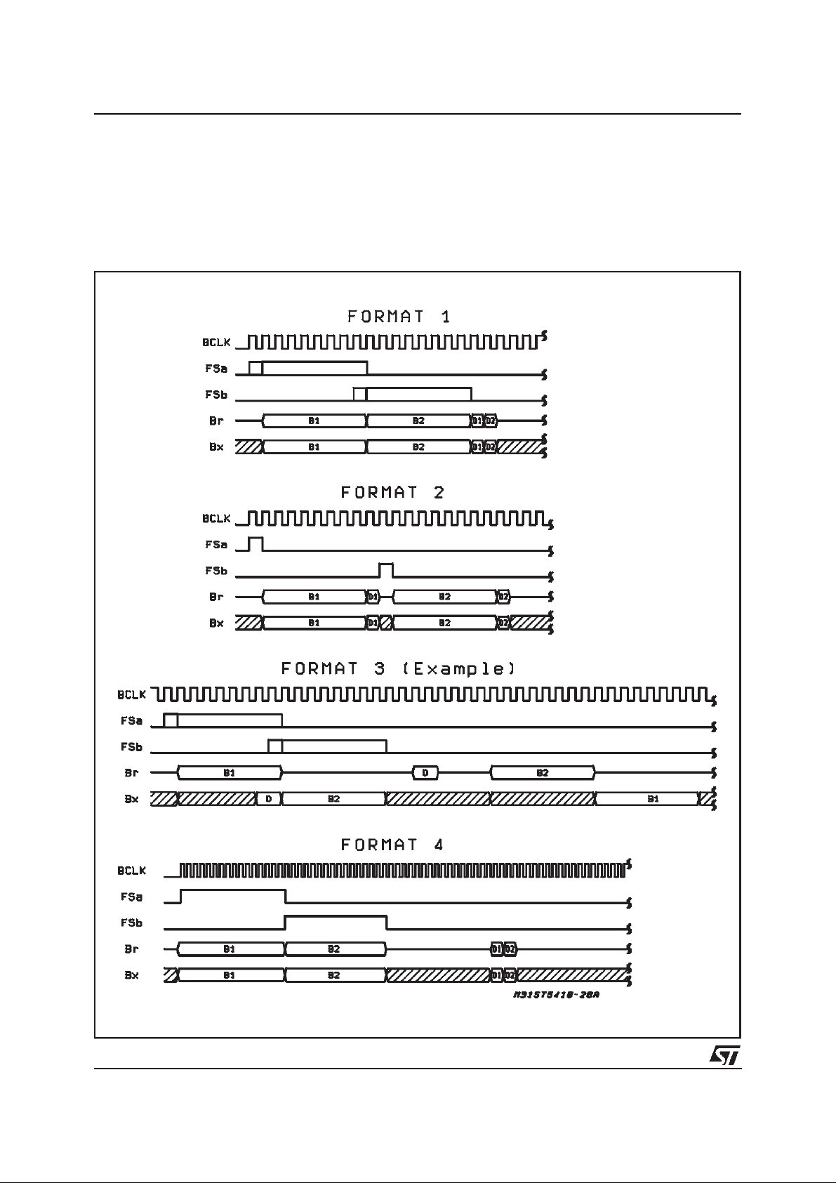
STLC5412 provides a choice of four multiplexed
formats for the B and D channels data as shown
in fig.2 and 3.
Format 1: the 2B+D data transfer is assignedto
the first18 bits of the frame on Br and Bx I/0 pins.
Channels are assigned as follows: B1(8 bits),
B2(8 bits), D(2 bits), with the remaining bits ignored until thenext Framesync pulse.
Format 2: the 2B+D data transfer is assignedto
the first 19 bits of the frame on Br and Bx I/O
pins. Channels are assigned as follows: B1(8
bits), D(1 bit), 1 bit ignored, B2(8 bits), D(1 bit),
with the remaining bits ignored until the next
frame sync pulse.
Format 3: B1 and B2 Channels can be independently assigned to any 8 bits wide time slot
among 64 (or less) on the Bx and Br pins. The
transmit and receive directions are also independent. When TDM mode is selected, the D
channel can be assigned to any 2 bits wide time
slot among 256 on the Bx and Br pins or on the
Dx and Dr pins (D port disabled or enabled in
TDM mode respectively).
Format 4: is a GCI like format excluding Monitor
channel and C/I channel.The 2B+D data transfer
is assigned to the first 26 bits of the frame on Br
and Bx I/O pins. Channels are assigned as follows. B1(8 bits) B2(8 bits), 8 bits ignored, D(2
bits), with remaining bits ignored up to the next
frame syncpulse.
When the Digital Interface clocks are selected as
inputs, FSa must be a 8 kHz clock input which indicates the start of the frame on the data input pin
Bx. When the Digital Interface clocks are selected
as outputs, FSa is an 8 kHz output pulse conforming to the selected format which indicates
the frame beginning for both Tx and Rx directions.
When the Digital Interface clocks are selected as
inputs, FSb is a 8 kHz clock input which defines
the start of the frame on the data ouput pin Br.
When the Digital Interface clocks are selected as
outputs, FSb is a 8 kHz output pulse indicating
the second 64kbit/s slot.
Two phase-relations between the rising edge of
FSa/FSb and the first (or second for FSb as output) slot of the frame can be selected depending
on format selected: Delayed timing mode or non
Delayed timing mode.
Non delayed data mode is similar to long frame
timing on the COMBOI/II series of devices: The
first bit of the frame begins nominally coincident
with the rising edge of FSa/b. When output, FSa
is coincident with the first 8 bits wide time-slot
while FSb is coincident with the second 8 bits
wide time-slot. Non delayed mode is not available
in format 2.
Delayed timing mode, which is similar to short
frame sync timing on COMBO I/II, in which the
FSa/b input must be set high at least a half cycle
of BCLK earlier the frame beginning. When output, FSa 1bit wide pulse indicates the first 8 bits
wide time-slot while FSb indicates the second.
Delayed mode is not availablein format4.
2B+D basic access data to transmit to the line
can be shifted in at the BCLK frequency on the
falling edges during the assigned time-slots.
When D channel port is enabled, only B1 & B2
data is shiftedin duringthe assigned time slots. In
format 4, data is shifted in at half the BCLK frequencyon the receive fallingedges.
2B+ D basic access data received from the line
can be shiftedout from the Br output at the BCLK
frequencyon the rising edges during the assigned
time-slots.Elsewhere,Br is in thehigh impedance
state. When the D channel port is enabled, only
B1 & B2 data is shiftedout from Br. In Format 4,
data is shifted out at half the BCLK frequency on
the transmit rising edges; there is 1.5 period delay
between the rising transmit edge and the receive
falling edge of BCLK.
15/74
Page 16
STLC5412
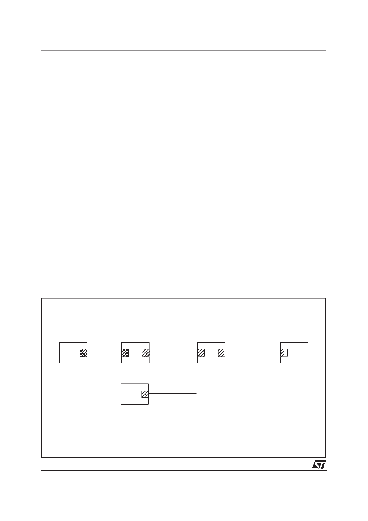
Bit Clock BCLK determines the data shift rate on
the Digital Interface. Depending on mode selected, BCLK is an input which may be any multiple of 8 kHz from 256 kHz to 6176 kHz or an output at a frequency depending on the format and
the frequency selected. Possible frequenciesare:
256 KHz, 512 KHz, 1536 KHz,
Figure 2: DSI Interfaceformats:MASTER mode.
2048KHz, 2560 KHz.
In format 4 the use of 256kHzis forbidden.
BCLK is synchronouswith FSa/b frame sync sig-
nal. When output, BCLK is phased locked to the
recoveredclock receivedfrom the line.
16/74
Page 17
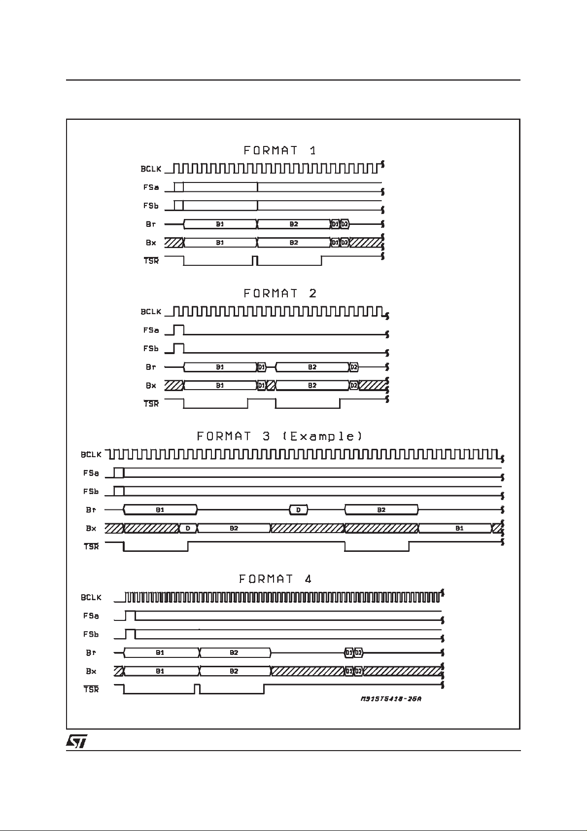
Figure 3: DSI Interfaceformats:SLAVE mode.
STLC5412
17/74
Page 18
STLC5412
GCI MODE
The GCI is a standard interface for the interconnection of dedicated ISDN componentsin the different equipments of the subscriberloop:
In a Terminal, GCI interlinks the STLC5412, the
ISDN layer 2 (LAPD) controllerand the voice/data
processing componentsas an audio-processoror
a TerminalAdaptormodule.
In NT1-2, PABX subscriber line card, or central
office line card (LT), GCI interlinks the UID, the
ISDN Layer 2 (LAPD) controllers and eventually
the backplane where the channels are multiplexed.
In NT1, GCI interlinks SID-GCI and STLC5412,
via automode (NT1-auto). In Regenerators, GCI
links both STLC5412 UID in automode (NT-RRauto, LT-RR-auto). (See Fig. 4a)
Frame Structure
2B+D data and control interface is transferredin a
time-division multiplexed mode based on 8 kHz
frame structure and assigned to four octets per
frame and direction.(seefig.4b).
The 64 kbit/s channels B1 and B2 are conveyed
in the first two octets; the third octet (M: Monitor)
is used for transferring most of the control and
status registers;the fourth octet (SC: Signalling &
Control) contains the two D channel bits, the four
C/I (command/lndicate)bits controlling the activation/deactivation procedures, and the E & A bits
which support the handling of the Monitor channel.
Figure 4a: GCIconfigurationsof the UID.
These four octets per frame serving one ISDN
subscribers line form a GCI Channel. One GCI
channel calls for a bit rate of 256 kbit/s.
In NT1-2s or subscriber Line Cards up to 8 GCI
channels may be carried in a frame of a GCI multiplex. The bit rate of a GCImultiplex may be from
256 kbit/s and up to 3088 kbit/s. Adjacent 4-octet
slots from the frame start are numbered 0 to 7.
The GCI channel takes the number of the slot it
occupies.Spare bits in the frame beyond 256 bits
from the frame start will be ignored by GCI compatible devices but may be used for other purposes if required (see Fig.4c). GCI channel number is selectedby biasing pins S0,S1,S2.
Physical Links
Four physical links are usedin the GCI.
Transmitteddata to the line: Bx
Receiveddata from the line: Br
Data clock: BCLK
Frame Synchronizationclock: FSa
GCI is always synchronized by frame and data
clocks derived by any masterclock source.
A device used in NT mode can deliver clock
sources able to synchronize GCI, either directly,
or via a local Clock Generator synchronized on
the line by means of the SCLK 15.36 MHz output
clock. Frame clock and data clock could be independent of the internal devices clocks. Logical
one on the Br output is the high impedance state
while logical zero is low voltage. For E and A bits,
active state is voltage Low while inactive state is
high impedancestate.
Figure 4a: GCI configurations of the UID
TERMINAL
18/74
NT1 REPETOR
NT
PRIVATETERMINAL
OR NT1-2
U
LTNT-RR-AUTOLT-RR-AUTONT1-AUTOSID-GCISID-GCI
LINE TERMINATIONSU U
Page 19
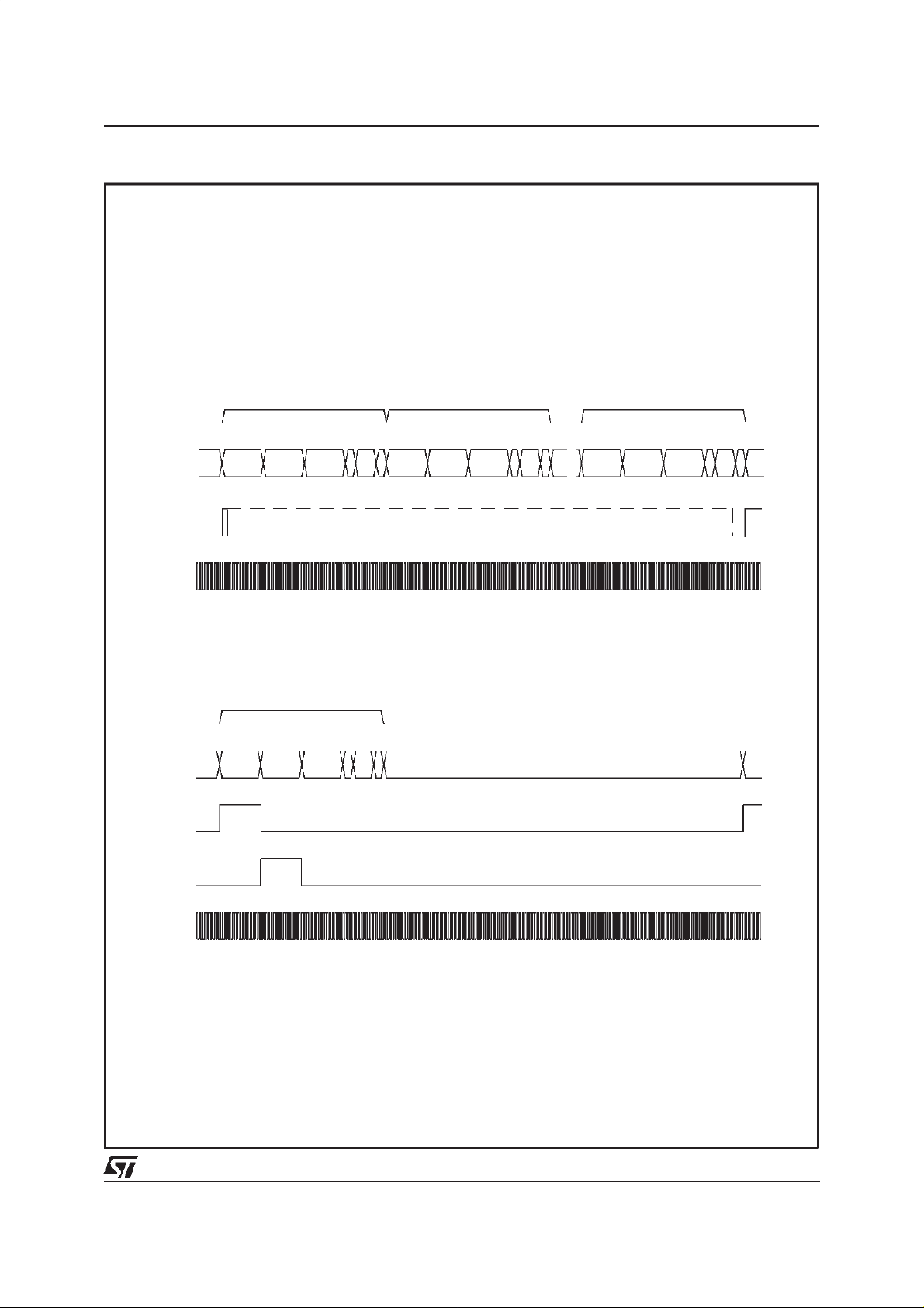
Figure 4b: GCI interfaceformat.
STLC5412
Figure 4b:
Bx/Br
FSa
BCLK
Bx/Br
GCI interface format
GCI CHANNEL 0 GCI CHANNEL 1 GCI CHANNEL 7
B1 B2 M D C/I A E
88 8242
8 KHz
GCI CHANNEL 0
B1 B2 M D C/I A E
8 8 8 242
B1 B2 M D C/I A E
88 8242
SLAVE MODE
FREE
B1 B2 M D C/I A E
88 8242
FSa
FSb
BCLK
8 KHz
MASTER MODE (BCLK = 1.536MHz)
MASTER MODE
19/74
Page 20

STLC5412
Figure 4c: GCImultiplexexamples,(slavemode).
20/74
Page 21

STLC5412
Data is transmitted in both directions at half the
data clock rate. The information is clocked by the
transmitteron the front edge of the data clockand
can be accepted by the receiver after 1 to 1.5 period of the data clock.
The data clock (BCLK) is a square wave signal at
twice the data transmission frequency on Bx and
Br with a 1 to 1 duty cycle. The frequencycan be
choosen from 512 to 6176 kHz with 16 kHz
modularity. Data transmission rate depends only
on the data clock rate.
The Frame Clock FSa is a 8 kHz signal for synchronization of data transmission. The front edge
of this signal gives the time reference of the first
bit in the first GCI input and output channel, and
resetthe slot counterat the startof each frame.
When some GCI channels are not selected on
devices connected to the same GCI link, these
time slots are free for alternativeuses.
GCI configuration selection is done by biasing of
input pins MW, M0, CONF1,CONF2 according to
Table1.
Table 1: GCIConfigurationselection.
Pin Number
PLCC44 DIP28 LT/NT12 (1) NT/TE NT1-AUTO LT-RR-AUTO NT-RR-AUTO
4328MW00000
4227M001111
27 19 S1/CONF1 S1 0 1 1 0
25 17 S2/CONF2 S2 1 1 0 0
10 7 S0/FSb/TEST2 S0 FSb TEST2 TEST2 TEST2
Pin name
Configuration
26 18 IO1/ES1 (2) IO1 IO1 ES1 PLDD ES1
24 16 IO2/ES2 (2) IO2 IO2 ES2 EC ES2
23 15 IO3/EC (2) IO3 IO3 EC LFS LFS
22 14 IO4/TEST1 (2) IO4 IO4 TEST1 TEST1 TEST1
35 22 SFSx/RFS (2) SFSx SFSx SFSx RFS RFS
(1) Differentationbetween LTand NT configurationdone by bit NTS in CR2 register;GCIin slave mode.
When NT1-AUTO or NT-RR-AUTO configuration is selected, BCLK bit clock frequency of 512 kHz is
automaticallyselected
When NT configurationis selected,BCLK bit clock frequencyof 1536 kHzis automaticallyselected.
(2) Connectedto V
throughinternal pull-upresistors.
CC
21/74
Page 22

STLC5412
Monitor channel
The Monitor channel is used to write and read all
STLC5412 internal registers. Protocol on the
Monitor channel allows a bidirectional transfer of
bytes between UID and a control unit with acknowledgement at each received byte. Bytes are
transmitted on the Br output and received on the
Bx input in theMonitorchanneltime slot.
A write or read cycle is always constituted of two
bytes.(see fig. 5). It is possible to operate several
write or read cycles within a single monitor message.
Note: Special format is used for EOC channel.
Write cycle
The format to write a messageinto theUID is:
A7 A6 A5 A4 A3 A2 A1 A0
1st byte
D7 D6 D5 D4 D3 D2 D1 D0
2nd byte
A7-A1:
A0:
D7-D0:
RegisterAddress
Write/Readback Indicator
RegisterContent
After the first byte is shifted in, Register address
is decoded. A0 set low indicates a write cycle: the
content of the following received byte has to be
loaded intothe addressedregister.
A0 set high indicates a read-back cycle request.
The second byte content is not significative.
STLC5412 will respond to the request by sending
back a message with the register content associated with its own address. It is then possible for
the microprocessor to receive the required register content after several other pendingmessages.
To avoid any loss of data, it is recommended to
operate only one read-backrequestat a time.
Note: Special format is used for EOC channel.
Read cycle
When UID has a register content to send to the
controller, it send it on the monitor channel directly. Note that the data to send can be the content of a Register previously requested by the
controllerby meansof a read-backrequest.
The format of the messagesent by the UID is:
A7 A6 A5 A4 A3 A2 A1 A0
1st byte
D7 D6 D5 D4 D3 D2 D1 D0
2nd byte
A7-A1:
A0:
RegisterAddress
forced to 0 if spontaneous
interrupt,forcedto 1 if readback
D7-D0:
RegisterContent
ExchangeProtocol
STLC5412 validates a received byte if it is detectedtwo consecutive times identical.(see fig. 5)
The exchange protocol is identical for both directions. The sender uses the E bit to indicate that it
is sending a Monitor byte while the receiver uses
A bit to acknowledge the received byte.When no
message is transferred,E bit and A bit are forced
to inactive state.
A transmission is started by the sender (Transmit
section of the Monitor channel protocol handler)
by putting the E bit from inactive to active state
and by sending the first byte on Monitor channel
in the same frame. Transmission of a message is
allowed only if A bit sent from the receiver has
been set inactive for at least two consecutive
frames. When the receiver is ready, it validates
the incoming byte when received identical in two
consecutive frames. Then, the receiver set A bit
from the inactive to the active state (preacknowledgement) and maintain active at least in the followingframe (acknowledgement).
If validation is not possible (two last bytes received are not identical) the receiver aborts the
message by setting the A bit active for only a single frame.The second byte can be transmitted by
the sender putting the E bit from the active to the
inactivestate and sending the second byte on the
Monitor channel in the same frame . The E bit is
set inactive for only one frame. If it remains inactive more than one frame, it is an end of message. The second byte may be transmittedonly
after receiving of the pre-acknowledgementof the
previous byte . Each byte hasto be transmittedat
leastin two consecutiveframes.
The receiver validates the current received byte
as for the first one and then set the A bit in the
next two frames first from the active state to the
inactivestate (pre-acknowledgement)and back to
the active (acknowledgement).If the receivercannot validates the received current byte (two bytes
received not identical)it pre-acknowledges normally but let the A bit in the inactive state in the
next frame which indicates an abort request . If a
message sent by the UID is aborted,the UID will
send again the complete message until receiving
of an acknowledgement . A message received by
the UID can be acknowledged or aborted with
flow Control.
The most significant bit (MSB) of Monitor byte is
sent first on the Monitor channel. E & A bits are
active low and inactive state on Br is 5 V. When
no byte is transmitted, Monitor channel time slot
22/74
Page 23
STLC5412
on Br is in the high impedance state.
A 24 ms timer is implemented in the UID. This
timer (when enabled) starts each time the sender
starts a byte sending and waits for a pre acknowledgement.
C/I channel
The C/I channel is used for TXACT and RXACT
registers write and read operation. However, it is
possible to access to ACT registers by monitor
channel: this access is controled by the CID bit in
CR2 register.
The four bits code (C1,C2,C3,C4) of TXACT register can be loaded in the UID by writing permanently this code in the C/I channel time-slot on Bx
input every GCI frames. The UID takes into account the received code when it has been received two consecutive times identical. When a
status change occurs in the RXACT register, the
new (C1,C2,C3,C4) code is sent in the C/I channel time-slot on Br output every GCI frames. This
code is sent permanently by the UID until a new
status change occurs in RXACTregister.
C1 bit is sent first to the line.
Figure 5: GCI Monitor channelmessaging examples.
LINE CODING AND FRAME FORMAT
2B1Q coding rule requires that binary data bits
are grouped in pairs so called quats (see Tab.2).
Each quat is transmitted as a symbol, the magnitude of which may be 1 out 4 equallyspaced voltage levels (see Fig. 6). +3 quat refers to the
nominal pulse waveform specified in the ANSI
standard. Other quats are deduced directly with
respect of the ratio and keeping of thewaveform.
The frameformatused in UID follows ANSI specification (see Tab. 3 and 4). Each complete frame
consists of 120 quats, with a line baud rate of 80
kbaud, giving a frame duration of 1.5ms. A nine
quats lenght sync-word defines the framing
boundary. Furthermore,a Multiframeconsistingof
8 frames is defined in order to provide sub-channels within the spare bits M1 to M6. Inversion of
the syncword defines the multiframe boundary. In
LT, the transmit multiframe starting time may be
synchronizedby meansof a 12 ms period of time
pulse on the SFSx pin selected as an input (bit
SFS in CR2); If SFSx is selected as an output,
SFSx provides a square wave signal with the rising edge indicatingthe multiframe startingtime.
In NT, the transmit multiframe starting time is pro-
Tx M
Tx
Tx E
Tx
Rx A
Rx
XM1
Tx
Tx M
Tx E
Tx
Rx A
Rx
fora message
XM1M1
1st byte
(M1)
Ready for
a message
pre-ack ack
(M1) (M1)
TWO BYTES MESSAGE ABORTED ON THE SECOND AND RETRANSMITTED
M1 M2 M2
1st byte
(M1)
pre-ack ack
(M1)
TWO BYTES MESSAGE- NORMAL TRANSMISSION
M2 M2
2nd byte
(M2)
2nd byte
(M2)
(M1)
X
pre-ack abort
(M2) (M2)
E & A BITS TIMING
pre-ack ack
(M2) (M2)
XX
3rd byte??
(X)
Ready for
retransmission
XXX
3rdbyte??
(X)
EOM
(or abort ack)
EOM
pre-ack??
(X)
X
Ready forReady
M1 M1 M2
1st byte
(M1)
pre-ack
(M1)
23/74
Page 24

STLC5412
vided on SFSx output by the rising edge of a 12
ms period square wave signal. LT or NT, when
pin 25 is selected as SFSr by mean of bit ESFr in
CR4, SFSris a square wave open drain output indicating the received superframeon the line. (see
figure 7). Prior to transmisssion, all data, with the
exception of the sync-word,is scrambled using a
self-synchronizingscramblerto perform the specified 23rd-order polynomial. Descrambling is included in the receiver. Polynomial is different depending on the direction LT to NT or vice versa.
TRANSMITSECTION
Data transmitted to the line consists of the 2B+D
channel data received from the Digital Interface
through an elastic data buffer allowing any phase
deviation with the line, the activation/deactivation
bits (M4) from the on-chip activation sequencer,
the CRC code plus maintenance data (eoc channels) and other spare bits in the overhead channels (M4, M5, M6). Data is multiplexed and
scrambled prior to addition of the sync-word,
which is generated within the device. A pulse
waveform synthesizer then drives the transmit filter, which in turn passes the line signal to the line
driver. The differential line-driver outputs, LO+,
LO- are designed to drive a transformer through
an external termination circuit. A 1:1.5 transformer designed as shown in the STLC5412 user
guide, results in a signal amplitude of 2.5V pk
nominal on the line for single quats of the +3
level. (see output pulse template fig.8). Short-circuit protection is included in the output stage;
over-voltage protection must be provided externally.
In LT applications, the Network reference clock
given by the FSa 8kHz clock input synchronizes
the transmitted data to the line. The Digital Interface normally accepts BCLK and FSa signals
from the network, requiring the selection of Slave
Mode in CR1. A Digital Phase-Locked Loop
(DPLL 1) on the UID allows the SCLK frequency
to be plesiochronous with respect to the network
reference clock (8 kHz FSa input). With a tolerance on the XTAL1 oscillator of 15.36 MHz +/100 ppm, the lock-in range of DPLL1 allows the
network clock frequency to deviate up to +/50ppm from nominal.
In LT, if DSI is selected in Master mode, (Microwire only, bit CMS = 1 in CR1), BCLK and FSa
signals are outputs frequency synchronized to
XTAL1 input, DPLL 1 is disabled.
In NT applications, data is transmitted to the line
with a phase deviation of half a frame relative to
the received data as specified in the ANSI standard.
RECEIVE SECTION
The receive input signal should be derived from
the transformer by a coupling circuit as shown in
the user guide. At the front end of the receive
section is a continuousfilter which limits the noise
bandwidth to approximately 100kHz. Then, an
analog pre-canceller provides a degree of echo
cancellationin order to limit the dynamic range of
the composite signal which noise bandwidth limited by a 4th order Butterworthswitched capacitor
low pass filter. After an automatic gain control, a
13bits A/D converter then samples the composite
received signal before the echo cancellation from
local transmitter by means of an adaptive digital
transversalfilter. The attenuationand distortionof
the received signal from the far-end, caused by
the line, is equalizedby a second adaptive digital
filter configured as a Decision Feedback Equalizer (DFE), that restores a flat channel response
with maximum received eye opening over a wide
spreadof cableattenuationcharacteristics.
A timing recovery circuit based on a DPLL(Digital
Phase-Locked Loop) recovers a very low-jitter
clock for optimum sampling of the received symbols. The 15.36MHz crystal oscillator (or the logic
level clock input) provides the reference clock for
the DPLL. In NT configuration,SCLK output provides a very low jitter 15.36MHz clock synchronized from the line.
Received data is then detected and flywheel synchronization circuit searches for and locks onto
the frame and superframe syncwords. STLC5412
is frame-synchronized when two consecutive
synchwords have been consecutively detected.
Frame lock will be maintained until six consecutive errored sync-words are detected, which will
cause the flywheel to attempt to re-synchronize.If
a loss of frame sync condition persists for 480ms
the device will cease searching, cease transmitting and go automatically into the RESET state,
ready for a further cold start. When UID is framesynchronized, it is superframe-locked upon the
first superframe sync-word detection. No loss of
superframesync-word is provided.
While the receiver is synchronized, data is descrambledusing the specified polynomial, and individual channels demultiplexed and passed to
their respective processing circuits: user’s 2B+D
channel data is transmittedto the Digital Interface
through an elastic data buffer allowing any phase
deviation with the line; the activation/deactivation
bits (M4) are transmitted to the on-chip activation
sequencer; CRC is transmitted to CRC checking
section while maintenance data (eoc) and other
sparebits in the overhead channels (M4, M5, M6)
are storedin their respective Rx registers.
In NT applications, if the Digital Interface is selected in master mode (see CR1) BCLK and FSa
clock outputs are phase-locked to the recovered
clock. If it is selected in Slave mode ie for NT1-2
application, the on-chip elastic buffers allow
BCLK and FSa to be input from an external
source, which must be frequency locked to thereceived line signal ie using the SCLK output but
24/74
Page 25

STLC5412
with arbitraryphase.
ELASTICBUFFERS
The UID buffers the 2B+D data in elastic fifos
which are 3 line-frames deep in each direction.
When the Digital Interface is a timing slave, these
FIFOs compensate for relative jitter and wander
between the Digital Interface and the line. Each
buffer can absorb wander up to 18µs at 80 KHz
max without ”slip”. This is particulary convenient
for NT1-2 or PABX application in case the local
reference clock is jitterized and wandered relative
to the incoming signal from the line.
DECT SYNCHRONIZATION
In a DECT system the U interface is used for digital transmissionbetweenthe base station controller (LT) and the base station (NT). The U interface allows the transmissionof 4 DECT channels
through B1, B2 using ADPCM compression. Beside the D channelallows the exchangeof signalling information between the base station controller (BSC)and the basestation(BS).
Seamless handover (for switching the radio-communication from one base station to another) requires additional features in U interface circuit for
base stationssynchronisation.
DECT OrientedFeatures In U Interface
Possibility to measure the round-trip delay between BSC and BS.
The different delay of each BSC-BS connection can be compensated in each BS with a
preset counter that is loaded with the delay
value provided by the STLC5412 in the BSC
and sentto theBS via the D channel.
Round trip delay (RTD) measurement allows to
estimate the link delay (SFSrNT-SFSxLT =
RTD/2+Konst) with a total accuracy of +/- 200
nsec whenSTLC5412is usedboth inBSC and
BS. The total accuracy is the sum of two contributions. The process spread on internal
propagation delays (±166.5ns) and jitter on recovered clock in LT (±32.5ns).
DECTframessynchronisation.
The BSC must synchronise all the BSs connected to itself. A synchronisation pulse DECSYNC is provided by the network to all the
STLC5412 devices in the BSC (LT). The
STLC5412 devices synchronise the 2B1Q
frames on the U link with DECSYNC and send
an EOC message to the corresponding BS
(NT). The STLC5412 in the BS (NT) on reception of the EOC message provides a pulse to
preset the counterfor DECT frame generation.
The jitter related to this pulse is the jitter of the
recovered clock in NT. Maximum jitter guaranteed onall ETSI loops is ±130ns.
These two features allow the BSC to generate
synchronous DECT frames (160ms) and multiframes with maximum phase difference of
±330ns.
LT DECT MODE
In LT DECT mode the STLC5412 provides round
trip delay estimation with a resolution of +/- 33
nsec. and automatic EOC DECT message transfer for base stations synchronisation.
The DECSYNC pulse is applied to pin SFSx
(CR2.7=0). The DECSYNC period must be multiple of 12ms and in phase with FSa. The SFSx input pulse resets the line framecounter when the
deviceis in power-up. After power-up, before activation, it is suggested to wait for the first available DECSYNC pulse. If not, the DECSYNC
pulse will generatea jump in the linesynchronisation, that cancause a line deactivation.
Round trip delay estimation procedure
The round trip delay is the delay between
Transmit sync word (ISW) and receive Sync
word on the line. It can be estimated from
three parameters that can be read in internal
registers:
tdd:totaldigital delay
delay between SFSx and SFSr in steps of 12.5
µsec.It is availablein registerDBAUD0-4
edd: elastic digital delay
value to add to tdd that takes into account the
internal elastic memory state. It is available in
registerDBAUD5-7
ced: clock elasticdelay
It providesthe phasedifference between transmit and receive clocks in steps of 65.1 nsec.It
is available in register DTXRX. See Application
Note for use.
DECTEOC message transfer
If CR7.0 = 1 (DECT mode) a synchronisation
pulse on pin SFSx triggers the DECT EOC
message transfer. The message stored in
DECTEOC register is transmitted 3 times in
the EOC channel starting from the 1st available superframefollowing the DECSYNCpulse
on theSFSx pin. See ApplicationNote for use.
NT DECT MODE
In NT DECT mode the STLC5412 after recognition of DECT EOCmessagestored in DECT EOC
register, generates a pulse on pin SFSx, synchronous with next SFSr edge. In this way the
STLC5412 provides on pin SFSx a pulse used to
resynchronise the DECT frame counter in the
base station.
TheLOCKbit in CR7 registercan be usedto enable
thelockingof FSawithSFSrafterlineisactivated.
In particular the FSa rising edge will occur 62.5us
after the SFSr rising edge.
25/74
Page 26

STLC5412
If not programmed this bit is inactive. The relock
will take place only after completion of present
monitor transfer. (EOM received). This locking will
cause a phase jump of FSa and BCLK signals. To
avoid problems on the GCI bus that is synchronized by FSa, a numberof 5 GCI frames after the
phase jump will be ignoredby the STLC5412.
For proper system operation before writing the
LOCK bit in CR7 register, the MOB bit (Mask
Overhead Bits) in CR4 register should be set to 1
to avoid spontaneous monitor message generation from STLC5412. Following the relocking the
MOB bit should be set back to desired value after
a minimumtime to be defined (ex. 1msec).
Thesuggestedprocedureis to programthe LOCKbit
in CR7 register after the AI indication from
STLC5412.In this case the system controller knows
whenthe phase jump takesplaceandcanresetthe
transmission/receptionoftheGCIcontroller.
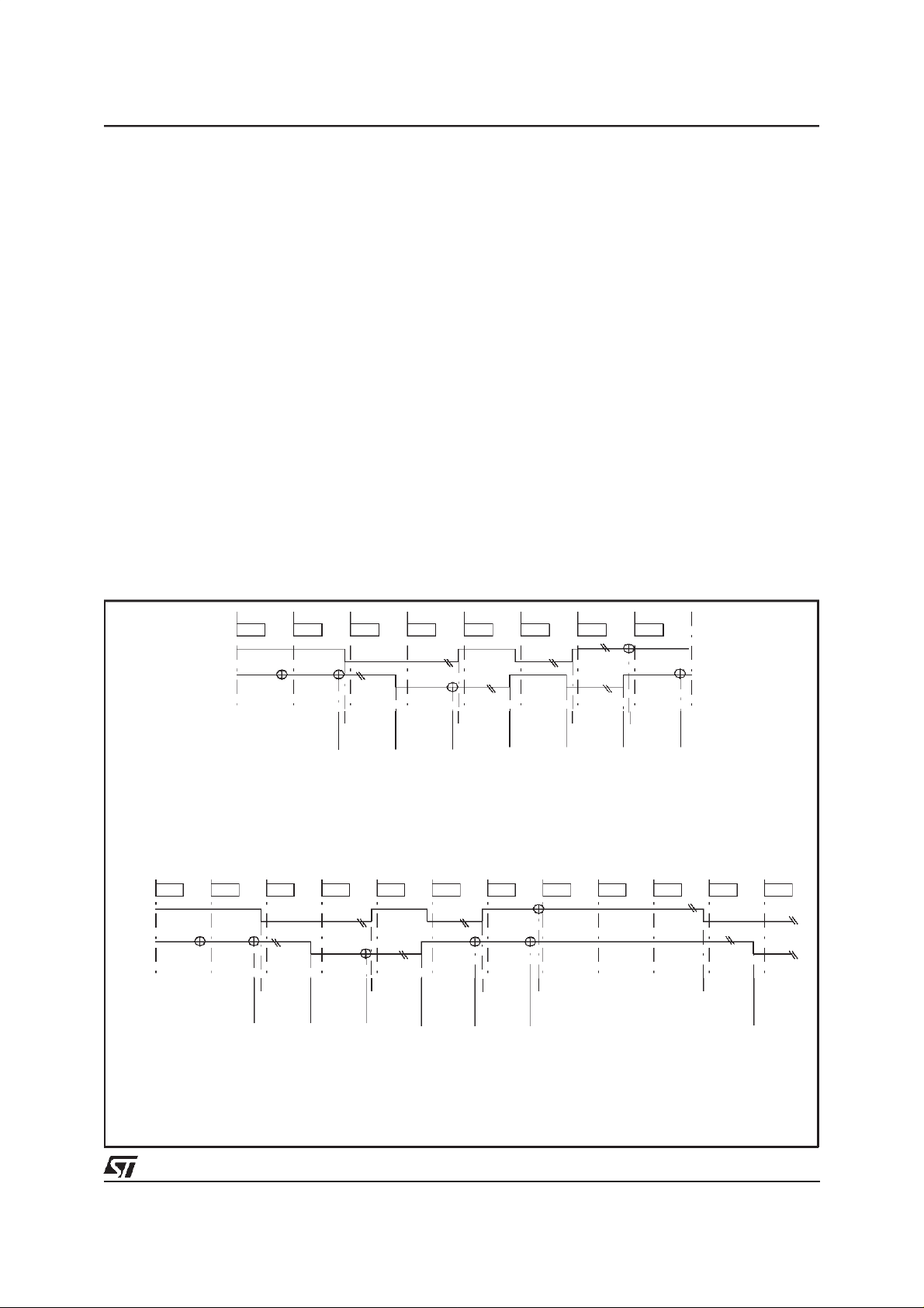
TIMING DIAGRAMS FOR DECT
LT DECT MODE
n*12ms (n=40 minimum)
Notes:
The DECT EOC message receptiongeneratesan
interrupt as a normal EOC message according to
the rules stored in OPR register. The DECT sync
message must be checked 3 times (reset value
of OPR register). If it is not detected3 times identical no pulse is generated. The DECT pulse
width on output pin SFSx is 6msec.
MAINTENANCE FUNCTIONS
M channel
In each frame there are 6 ”overhead”bits assigned
to various control and maintenance functions.
Some programmable processing of these bits is
provided on chip while interaction with an external
controller provides the flexibility to take full advantage of the maintenance channels. See OPR,
TXM4, TXM56, TXEOC, RXM4, RXM56, RXEOC
SFSx
TX EOC
SFSr
RX EOC
SFSx
DECT DECT DECTtxeoc
6ms
txeoc txeoc txeoc txeoctxeoc txeoc txeoc txeoc
NT DECT MODE
12 ms
DECT DECT DECTrxeoc
36ms + line delay
RXEOC INT
rxeoc rxeoc rxeoc rxeocrxeoc rxeoc
6ms
RXEOCINT
n*12ms
DECTDECTDECT
RXEOCINT RXEOCINT
DECTDECTDECT
rxeoc
rxeoc
26/74
Page 27

STLC5412
registers description for details. New data written to
any of the overheadbit Transmit Registers is resynchronized inter nal l y to the next available compl ete
superfram eorhalfsuperframe,asappropri ate.
Embedded OperationChannel(EOC)
The eoc channelconsists of two complete 12 bits
messagesper superframe,distributedthroughthe
M1, M2 and M3 bits of each frame. Each message is composed of 3 fields; a 3 bit address
identifying the message destination/origin, a 1 bit
indicator for the data mode i.e. encoded message
or raw data, and an 8 bits information field. The
Control Interface (Microwire or Monitor channel in
GCI) provides access to the complete 12 bits of
every message in TX and RX EOC registers.
Whennon-automode is selected,UID does not interpretthe received eoc messages e.g. ”send corrupted CRC”; therefore the appropriate command
instructionmust be written to the device e.g. ”set to
one bit CTC in registerCR4”.It is possibletoselect
a transparenttransmission mode in which the eoc
channelcanbeconsideredas atransparent2 kbit/s
channel.SeeOPR registerdescriptionfordetails.
When auto-mode is selected in GCI configuration,
UID performs automatic recognition / acknowledgement of the eoc messages sent by the network according to processing defined in ANSI
standardand illustrated in figure 9. When UID recognizes a message with the appropriate address
and a known command, it performs automatically
the relevant action inside the device and send a
message at the digitalinterfaceas appropriate.Table 5 givesthe listof recognizedeocmessagesand
associatedactions.
When NT-RR-AUTO configuration is selected,
eoc addressing is processed according to appendix E of T1E1.601standard:
– If address of the eoc message received from
LT is in the range of 2 to 6, UID decrements
address and pass the message onto GCI.
– If address of the eoc message received from
GCI is in the range of 1 to 5, UID increments
address and pass the message onto the line
towardLT.
– If data/msg indicator is set to 0, UID pass
data on transparentlywith eoc address as describedabove.
M4 channel
M4 bit positions of every frame is a channel in
which are transmitted data bits loaded from the
TXM4 transmit register and from the on-chip activation sequencer each superframe. On the receive side, M4 bits from one completesuperframe
are first validated and then stored in the RXM4
Receive Register or transmitted to on-chip activation sequencer. See OPR, TXM4 and RXM4 registers descriptionfor details.
When NT1-AUTO or NT-RR-AUTO mode is selected, bits ps1 and ps2 in M4 channel are controlled directly by biasing input pins ES1 and ES2
respectively. e.g. ps1 is sent continuously to the
line equal 0 when ES1 input is forcedat 0 Volt.
Spare M5 and M6 bits
The spare bit positions in the M5 and M6 field
form a channel in which are transmitted databits
loaded from the TXM56 transmit register. On the
receive side, the spare bits in the M5 and M6
field are first validated and then stored in the
RXM56 receive register. See OPR, TXM56 and
RXM56 registers description for details.
CRC calculation/checking
In transmit direction, an on-chip CRC calculation
circuit automaticallygenerates a checksum of the
2B+D+M4 bits using the specified 12th order
polynomial. Once per superframe, the CRC is
transmitted in the M5 and M6 bit positions. In receive direction, a checksum is again calculated
on the same bits as they are received and, at the
end of the superframe compared with the receivedCRC. The result of this comparison generates a ”Far End Block Error” bit (febe) which is
transmitted back towards the other end of the
Line in the next but one superframe and an indication of Near End Block Error is sent to the systemby meansof RegisterRXM56. If thereis no errorinsuperframe,febe is set= 1, and if thereis one
ormore errors, febeis set = 0.
UID also includes two 8 bits Block Error Counters
associated with the febe bits transmitted and received. It is then possible to select one Error
Counterper directionor to selectonly one counter
forbothby meansof bit C2E in OPR register.Block
errorcountingis always enabledbut it is possibleto
disabled the threshold interrupt and/or to enable/disablethe interruptissuedat eachreceivedor
transmittedblockerror detection.See OPR register
fordetails.
Loopbacks
Six transparent or non transparent channel loopbacksareprovidedby UID. It is thereforepossible to
operateanyloopbackon B1, B2 and D channelsline
to line or DSI/GCI to DSI/GCI. Command are
groupedinCR3regis te r.
In addition to the channel loopbacks in LT modes,
a complete transparent loopback operated at the
transmission side of UID allows the device to activate through an appropriate sequence with the
complete data stream looped-back to the receiver. Therefore,most of analog/digitalclockand
data recovery circuits are tested. After activation
completed, an AI status indication is reported.
Completeloopbackis enabledwith ARL command
in TXACTregister.
27/74
Page 28

STLC5412
Table 2: 2B1Q Encoding of 2B+ D Fields.
Time
11b12
1
→
b13b
q
B
I
b15b
14
2
q
b17b
16
3
q
b21b
18
4
22
q5 q
b23b
B
g
b25b
24
6
q
b27b
26
7
28
q
8
Data
Bit Pair b
Quat # (relative) q
# Bits 8 8 2
# Quats 4 4 1
Where:
b
= first bit of B1octet as received at the S/T interface
11
= last bit of BIoctet as received at theS/T interface
b
18
b
= first bit of B2octet as received at the S/T interface
21
= last bit of B2octet as received at theS/T interface
b
28
d
= consecutive D-channel bits(d1is first bit of pair as received at the S/T interface)
1d2
q
= ith quat relative tostart of given 18-bit2B+D data field.
i
NOTE: There are 12 2B+D 18-bitfieldsper 1.5 msec basic frame.
Table 3: Network-to-NT2B1Q Superframe Technique and Overhead Bit Assignments.
d1d
q
D
2
9
FRAMING
2B+D Overhead Bits (M
1-M6
)
Quat Positions 1-9 10-117 118s 118m 119s 119m 120s 120m
Bit Positions 1-18 19-234 235 236 237 238 239 240
Super Basic
Frame Frame
# # Sync
2B+D M
1
M
2
M
3
M
4
M
5
M
Word
A 1 ISW 2B+D eoc
2 SW 2B+D eoc
3 SW 2B+D eoc
4 SW 2B+D eoc
5 SW 2B+D eoc
6 SW 2B+D eoc
7 SW 2B+D eoc
8 SW 2B+D eoc
dm
dm
eoc
a1
eoc
i3
i6
a1
eoc
eoc
eoc
eoc
i3
i6
eoc
eoc
eoc
a2
i1
i4
i7
a2
i1
i4
i7
eoc
eoc
eoc
eoc
eoc
eoc
eoc
a3
i2
i5
i8
a3
i2
i5
i8
act 1 1
dea 1 febe
1crc
1crc
1crc
1crc
uoa crc
aib crc
1
3
5
7
9
11
crc
crc
crc
crc
crc
crc
B,C,...
NT-to-Network superframe delay offset from Network-to-NT superframe by 60
±
2 quats (about 0.75
ms).All bits than the Sync Word are scrambled.
Symbols & Abbreviations:
”1” reserve = reserved bit for future standard; set = 1 act activation bit
eoc embedded operations channel
a = address bit
dm = data/message indicator
i = information (data/message)
SW synchronization word febe far end block error bit (set = 0 for errored
ISW inverted synchronization word dea deactivation bit (set = 0 to announce deactivation)
s sign bit(first) in quat uoa u only activation bit (set = 1to activate S/T)
m magnitude bit (second) in quat aib alarm indication bit (set = 0 to indicate interruption)
crc cyclic redundancy check: covers 2B+D & M4
1 = most significantbit
2 = next most significant bit
etc
superframe)
6
2
4
6
8
10
12
28/74
Page 29

STLC5412
Table 4: NT-to-Network2B1Q Superframe Technique and Overhead Bit Assignments.
FRAMING 2B+D Overhead Bits (M1-M6)
Quat Positions 1-9 10-117 118s 118m 119s 119m 120s 120m
Bit Positions 1-18 19-234 235 236 237 238 239 240
Super Basic
Frame Frame
# # Sync Word 2B+D M
1 1 ISW 2B+D eoc
2 SW 2B+D eoc
3 SW 2B+D eoc
4 SW 2B+D eoc
5 SW 2B+D eoc
6 SW 2B+D eoc
7 SW 2B+D eoc
8 SW 2B+D eoc
1
a1
dm
i3
i6
a1
dm
i3
i6
M
eoc
eoc
eoc
eoc
eoc
eoc
eoc
eoc
2
a2
i1
i4
i7
a2
i1
i4
i7
2,3,...
NT-to-Networksuperframe delayoffset from Network-to-NTsuperframeby 60 ± 2 quats (about 0.75 ms).
All bitsthan the Sync Word are scrambled.
Symbols & Abbreviations:
M
eoc
eoc
eoc
eoc
eoc
eoc
eoc
eoc
3
a3
i2
i5
i8
a3
i2
i5
i8
M
4
act 1 1
ps
1
ps
2
ntm crc
cso crc
1 crc
sai crc
1 crc
M
5
1 febe
crc
1
3
5
7
crc
9
11
crc
M
crc
crc
crc
crc
6
2
4
6
8
10
12
”1” reserve = reserved bit for future standard; set = 1 ps1,
eoc embedded operations channel
power status bits (set = 0 to indicate power
ps
problems)
2
ntm NT in Test Mode bit (set = 0 to indicate test mode
a = address bit
dm = data/message indicator
i = information (data/message)
SW synchronization word cso cold-start-only bit (set = 1 to indicate cold-start-only
ISW inverted synchronization word crc cyclic redundancy check: covers 2B+D & M4
1 = most significantbit
2 = next most significant bit
etc
s sign bit(first) in quat febe far end block error bit (set = 0 for errored
superframe)
m magnitude bit (second) in quat sai S/T interface activation indication bit.
act activation bit
Figure 6: Exampleof 2B1Q Quaternary Symbols.
29/74
Page 30

STLC5412
Figure 7: SuperframeI/O pin SFS
30/74
Page 31

Figure 8: Normalizedoutput pulse form
STLC5412
31/74
Page 32

STLC5412
Figure 9: EOCmessageprocessingmode.
32/74
Page 33

Figure 10: CRCErrors Processing(auto-mode)
STLC5412
33/74
Page 34

STLC5412
Table 5: EOC message processing:local actions.
NT1-AUTO: (eoc address 000or 111)
Message Code Local action
Operate 2B+D loopback
Operate B1channel Loopback
Operate B2 channel Loopback
Request Corrupted CRC
Notify of Corrupted CRC 0101 0100 Noaction taken.Sendbacktothe Networkunableto complymessage.
Return to Normal 1111 1111 All outstanding EOC operations are reset.
Hold state 0000 0000 All outstanding EOC operations maintained in their present state
Unable to comply 1010 1010 Sent by UID to indicate that the message is not in its menu
NT-RR-AUTO: (eoc address 001 or 111)
Message Code Local action
Operate 2B+D loopback
Operate B1channel Loopback
Operate B2 channel Loopback
Request Corrupted CRC
Notify of Corrupted CRC 0101 0100 Noactiontaken.Sendback totheNetwork unable tocomply message.
Return to Normal 1111 1111 All outstanding EOC operations are reset.
Hold state 0000 0000 All outstanding EOC operations maintained in their present state
Unable to comply 1010 1010 Sent by UID to indicate that the message is not in its menu
0101 0000
0101 0001
0101 0010
0101 0011
0101 0000
0101 0001
0101 0010
0101 0011
Send ARL code on C/I channel to operate Loopback 2 in SID-GCI.
Forces EC output low
Performs transparent loopback on B1 channel identical to LB1
command in CR3
Performs transparent loopback on B2 channel identical to LB2
command in CR3
Performs corruptionof the transmit CRC identical to CTC
command in CR4.
Send ARL code on C/I channel to operate Loopback 1A in UID
configured in LT-RR-AUTO. Forces EC output low.
Performs transparent loopback on B1 channel identical to LB1
command in CR3
Performs transparent loopback on B2 channel identical to LB2
command in CR3
Performs corruptionof the transmit CRC identical to CTC
command in CR4.
IDENTIFICATION CODE (GCI)
The identification register is implemented at the
two addresses80 H and 90H. Allaccessesat addresses 8x H will generate a read back interrupt
containing the addresses80 H. Accesses at 9x H
performs exactly the same thing thatthe 8X register except the interruptwill be at address 90 H.
Response will be according to therule herebelow:
identification request: 1 0 0 Y X X X X X X X X X X X X
identificationresponse: 100YCCCCTTDDDDDD
with: - C = circuit revision
-T=devicetype(U=00)
- D = device level identifyingthe manufacturer (001000 for
SGS-THOMSON Microelectronics)
-Y = don’t care
In particular for 1.0 version the identification response is:
100Y0000 00001000
For 1.1 versionthe identificationresponseis:
100Y0101 00001000
34/74
GENERALPURPOSE I/Os (GCI)
When GCI non-automode is selected,(NT orLT),
four programmable I/Os (IO1, IO2, IO3, IO4) are
provided and associated with CR5 register. Each
I/O is internalIy pulled-up with a 250kΩ resistor.
Input or output can be selected for eachpin independently from the others by means of bits IO1,
IO2, IO3, IO4 in CR5. D1, D2, D3, D4 bits give
the logical value of the I/O pins respectively.
When a status change occurs on one of the input
pins, CR5 is sent on the monitor channel of the
GCI interface.
When GCI auto-mode is selected, two inputs
(ES1, ES2) and one output (EC) are provided in
NT1-AUTOand NT-RRAUTO configurationsonly.
ES1 and ES2 inputs drive the logical values of
ps1 and ps2 bits in the M4 channel on the line
while EC ouput normally high is driven low using
the eoc message ”operate 2B+D loopback. This
intends to provide power supply testing command
occuring simultaneously with the loopback command.
Page 35

STLC5412
TEST FUNCTIONS
Varioustest functionsare provided for transmitted
pulse waveform checking, power spectral density
measurementandtransmitterlinearity.
Three commands in TXACTregister are provided.
The associated test function is enabled as long as
the command is not disabled by any other command.
SP1: (0010) Send Single Pulses+1,-1:
+1, -1, pulses are transmitted consecutively onto
the line, one pulse per frame.
SP3: (1011) Send Single Pulses+3,-3:
+3, -3, pulses are transmitted consecutively onto
the line, one pulse per frame.
RDT: (0011) Random Data Transmitted:
Random data can be transmitted onto the line
continuously. B1, B2 and D channeltransparency
between the digital interface and the line is enabled.
When auto-mode is selected, two test inputs
(TEST1, TEST2) are provided allowing the same
test functions as describedabove but without the
need of a microcontroller. See Table 6 for Test
pins biasing.
MONITOR channel depending of CID bit in CR2
register)is used in GCI mode.
In MICROWIRE mode, a primitive indication generates first an interrupt requesting an action from
the Microprocessor, in GCI mode the primitive Indication is directly transmitted via C/I (or MONITORchannel).
Power on initialization
Following the initial application of power,
STLC5412 enters the power down deactivated
state in MICROWIRE mode or in GCI mode dependingon thepolarizationof theMW input.
All the internal circuits including the master oscillator are inactive and in a low power state except
for the 10 kHz Tone signal detector. The line outputs LO+/LO- are low impedance and all digital
outputs are high impedance. All programmable
registers and the activation controller are reset to
their default value.
GCI configuration is defined by means of the configuration pins M0, CONF1 and CONF2 when
Power supply is turned on.
For LT and NT1-2 equipments,GCI configuration
should be completed by means of Control Register Programming. See Table 1 for configuration
pins bias.
Table 6: Test Pins
TEST1 TEST2 FUNCTIONS
1 1 Normal operation
1 0 Send Single Pulse±1
0 1 Random Data Transmitted
0 0 Send Single Pulse ± 3
TURNING ON AND OFF THE DEVICE
STLC5412 contains an automatic sequencer for
the complete control of the start-up activation sequences. Interactions with an external control unit
requires only Activate Request and Deactivate
Request commands, with the option of inserting
break-points in the sequence for additionalexternal control allowing for instance easy building of a
repetor application. Automatic control of act,
uoa/sai and dea bits in the M4 bit positionsis provided, along with the specified40 ms, 480 ms and
15 s timers used during the sequencing.
Except the Power up and Power down control
that is slightly different, the Activation/Deactivation procedures are identical in GCI and Microwire/DSI modes. Same command codes or indication codes are used. In Microwire and GCI
mode, activation control is done by writing in the
Activation Control Register TXACT and by reading the Activation Indication Register RXACT. For
TXACT and RXACT access, MICROWIRE port is
used in MICROWIRE mode and C/I channel (or
Line signal detection
When UID is in the power down state and a
10kHz tone TN or TL is detected from the line
LSD and INT (MICROWIRE/DSI only) open drain
outputs are forcedto zero.
In NT configuration, code LSD (0000) is loaded
in the activationindication register RXACT.
In LT configuration, code AP (1000) is loaded in
the activationindicationregisterRXACT.
In Microwire/DSI these indications are sent onto
CO at the following access even if the UID is still
in power down mode.
In GCI these indications are sent onto the C/I
channel as soon as GCI clocksare available.
LSD open drain output is set back in the high impedance stateas soon as theUID is poweredup.
INT open drain output is set back in the high impedance statewhen CSinput is detectedat zero.
Depending of the ACTAUT and PUPAUT bits in
CR6 register, UID can powered up itself, also
automaticallytostartthe activation.
For all auto mode configurations, on 10KHz tone
reception, power up and activation procedure are
full automatic, but in NT1 auto, UID waits the uoa
bit from the line before to provide (or not) the
cloks and primitives to the S device.
Power up control
Microwire/DSI: control instruction PUP in ACT
35/74
Page 36

STLC5412
registeris requiredto power up the UID.
GCI:whenGCI ”NT masteroftheclocks”configura-
tion is selected, UID provides the GCI clocks
neededfor controlchanneltransfer;PUPcontrolinstruction is provided to the UID by pulling low the
Bx data input; STLC5412 then reacts sendingGCI
clocks. It is possible to operatean automaticpower
up of the UID when a wake up tone is detected
from theline by connectingthe LSD outputdirectly
to theBxinput.
GCI: when NT1-2 or LT configuration is selected
(M0 = 0), the UID is powered up after configuration settingby the PUP code (0000)on C/I Channel.
Power down control
A control instruction PDN in ACT register is required to power down the device after a periodof
activity. PDN forces directly the device to the low
power state without sequencing through any of
the de-activation states. It should therefore only
be used after the UID has been put in the line deactivated state. PDN has no influenceon the content of the internal registers, but immediately
stops the output clocks when UID is in master
mode and inµW/DSI mode.
In GCI mode, UID send first two times code
DI(1111) on C/I channel before powering down at
the end of the assignedGCI channel.
The DI code purpose is similar to PDN code but
power down state is enteredonly when the line is
entirely deactivated (state H1 or J1). The DI command is recommended.
Power up state
Power up transition enables all analog and digital
circuitry, starts the crystal oscillator and internal
clocks. The LSD output is in the high impedance
state even if a tone is detected from the line. As
for PDN, PUP has no influence on the content of
the internal registers
Power down state
Following a period of activity in the power up
state, the power down state may be re-entered as
describedabove.ConfigurationRegistersremainin
their current state. PDN and DI have no influence
on the content of the internal registers: it is then
possible, for instance, after a normal deactivation
procedure followed by a power down command,to
power up again the device in order to operatedirectlya WarmStart procedure.
CASE OF RESTRICTEDACTIVATION
The standard specifies a mode where the U interface can be turnedon without the need to activate
theS/Tinterfaceprovidedthisfunctionis supported
at both ends of the loop. In this conditionMaintenance channel is available, typically for setting
loop-backsinthe NT forerror ratetestingandother
diagnostics.
When this mode is enabled,bit M47 on the line in
LT to NT direction becomes the uoa bit. Setting
UAR activation command in the LT chip will set
uoa bit equal zero on the line. Detection of uoa bit
equal zero by the NT will inhibit activation of the
S/T interface. This results in SN3 signal in the NT
to LT direction, which causes generation of UAI
indication by the LT U device when superframe
synchronized.
If during restricted activation operation, a TE
starts to try activate the S/T interface by sending
info 1, theNT can pass this request to the LT via
M47 bit, the sai bit. This bit is set equal one by
writing AR command to the Activation Control
Register. sai bit received equal one causes generationof an AP indication by the LT U device.
RESETOFACTIVATION/DEACTIVATION STATE
MACHINE
When the device is either powered-upor down, a
control instruction RES resets the activation controller ready for a cold start. That feature can be
used if the far-end equipment fails to warm start,
for example if the line card or NT has been replaced or if in a regenerator, the loss of synchronisation of the second section imply the reset of
the first section for a further cold start. The configurationregistersremain in their selectedvalue.
HARDWARE RESET
When GCI configurationis selected, pin RES acts
as a logical hardware Reset. The device is entirely reset including activation/deactivation state
machine and configuration registers. Configuration pins bias excluding MW define the eventual
new configuration.Pin MW must be maintained at
the 0 Volt for GCI configurationsetting.
It is possible to operate a similar ”complete reset”
of UID by setting high bit RST in the RXOH command register. In this last case the Control interface remains enabled. Refer to User guide for
Softwarereset procedure.
ACTIVATION/DEACTIVATION SEQUENCING
Activation/deactivationsignals onto the line are in
accordance with the activation/deactivation state
matrixgiven in AppendixA.
36/74
QUIETMODE
It ispossible to forcethe device in a quiet mode in
which UID does not react to any line wake-up
tone and LSD pin remains high. There are two
Page 37

STLC5412
ways to enter quiet mode: QM bit in CR6 register
and QM primitive command to write in TXACT
register; in this last case, any further primitive will
clear quiet mode.
AUTOMODE
For all auto mode configurations,AIS pin allows a
choice of line interface: 27 or 15mH for the transformer and resistors line or device side.
In NT1, the activation/deactivationstate machine
and the automatic power-up / power-down capabilities of the UID provide for a direct connection
through GCI between UID and SID-GCI (ST
5421) without the need of an extra microcontroller
(seefigure 13b).LSD-pin of SID-GCImust be connectedtogetherto the Bx inputpinof UIDto ensure
autonomouspower-up/downcontrol.Activation/Deactivation commands and indications are transferredfromonedeviceto the otherby meansof the
C/I channel. Maintenancefunctions are automatically processed in UID. Therefore, there is no
transfer of messages on the Monitor channel between UID and SID-GCI. Please note that the
2B+D loop-back request at the S interface is provided using the C/I channel code ARL and that
there is not automaticprocessing of S and Q messagesin SID-GCI.
In Repetor, the same advantages are provided by
a direct connection through GCI between both
UID without the need of an extra microcontroller
(see figure 13c). As for NT1, C/I channel transfers
activation/deactivation commands and indications. Maintenance functions are automatically
processed in UIDs, needing the transfer of eoc
messages, overhead bits and CRC fault detections. This is performed autonomously on the
Monitor channel by sending when required messages in a regular format as already described.
eoc messages are transmitted according to Table
5; overhead bits in the M4 channel excluding act,
dea, uoa and sai, are transferred transparently;
spare overhead bits in M5 or M6 bit positions are
also transferred transparently; febe and nebe bits
are transmittedaccordingto Figure10.
COMMANDINDICATION (C/I) CODES
Activation, deactivation and some special test
functions can be initiated by the system by writing in TXACT register. Any status change of the
on-chip state machine is indicated to the system
by the UID by setting a new code in the RXACT
register. When GCI is selected, TXACT and
RXACT registers are normallyassociated with the
C/I channel (it is possible to associate them with
the MONITOR channel thank to the CID bit in
CR2 register). All commands and indications are
coded on four bits: C1, C2, C3, C4. Codes are
listed in Table 7. For each mode, a list of recognized commands and generated indications is
given. Hereafter, you have a detailed description
of the codesdependingon modeselected.
NT mode: Command
0000 (PUP): PowerUp
When in the power down state, PUP command
powers up the device ready for a cold or a warm
start. When GCI is selected with clocks as outputs, PUP command is replacedby pulling low Bx
input pin.
0001 (RES): Reset
RES command resets UID ready for a cold start.
Configurationregisters are not changed. RES can
be operated when the device is eitherpowered up
or down.
If RES command is applied when the line is not
fully deactivated,UID properly ends the activation
before to come back in H1 state; In this case DP
or EIU indication is returned (Auto mode configurationor not respectively).
0010 (SP1): SendSinglePulse+1 and -1
SP1 test command forces UID to send +1, -1,
pulsesto the line, one pulse per frame.
0011 (RDT):
RandomData Transmitted
RDT test command forces UID to send data with
randomequiprobablelevels at 80 kbaud.
0100 (EIS): Error Indicate S Interface
EIS command reports on the U line, a default on
the S interface.
0101 (PDN):
Power Down
PDNcommandforcesUID to power down state.It
should normally be used after UID has been set
in a known deactivated state, e.g. in an NT after a
DI status indication has been reported. In GCI, C/I
indication (DI) is sent twice on Br output before
UID powers down.
0110 (UAI): U interfaceActivationIndicate
UAI command is significant only when RR bit is
set equal one in CR2 register or if NT-RR-AUTO
auto-mode is selected. After the receiver has
been super-frame synchronized, UAI command
allows UID to send SN3 signal to the line.
0111 (QM): Quiet Mode
In this mode,UID doesnot react to any linestatus
change. UID can be powered up or down and
ready for a cold start or a warm start. All configuration registers and coefficients remain unchanged. Quiet Mode is disabled by any other
command.
Note: Inside UID, an logical or is implemented
with this QM primitiveand the QM bit in CR6 register.
1000 (AR): ActivationRequest
Beeing in the Power Up and deactivated state
37/74
Page 38

STLC5412
Table 7a:
Note:
(1) ONLY IN SLAVE MODE. INGCI MASTER MODE,SETBX PINTO ”0” TO DOA PUP..
RXACT(indication) and TXACT(command) codes
CODES
C4 C3 C2 C1
0 0 0 0 0 DP/LSD PUP (1) – PUP/DR
1 0 0 0 1 EIU RES EIU RES
2 0 0 1 0 – SP1 – SP1
3 0 0 1 1 – RDT – RDT
40100EIEIEIFA0
5 0 1 0 1 – PDN – PDN
6 0 1 1 0 – – UAI UAR
7 0 1 1 1 – QM – QM
81000APARAPAR
91001––––
A1010–––ARL
B 1 0 1 1 – SP3 – SP3
C1100AIAIAIAI
D1101––––
E 1 1 1 0 – AIL – –
F1111 DI DI DI DI
(GCI or MW, NON AUTO-MODE)
RXACT
(indications)
NT
TXACT
(commands)
(GCI or MW, NON AUTO-MODE)
RXACT
(indications)
LT
TXACT
(commands)
CODES
C4 C3 C2 C1
0 0 0 0 0 DP/LSD PUP (1) – PUP/DR
1 0 0 0 1 EIU RES EIU RES
2 0 0 1 0 – SP1 – SP1
3 0 0 1 1 – RDT – RDT
40100EIEIEIFA0
5 0 1 0 1 – PDN – PDN
6 0 1 1 0 UAP UAI UAI UAR
7 0 1 1 1 – QM – QM
81000APARAPAR
91001––––
A1010–––ARL
B 1 0 1 1 – SP3 – SP3
C1100AIAIAIAI
D1101––––
E1110––––
F1111 DI DI DI DI
(1) ONLY IN SLAVE MODE.
(GCI or MW, NON AUTO-MODE)
RXACT
(indications)
NTRR
TXACT
(commands)
(GCI or MW, NON AUTO-MODE)
RXACT
(indications)
LTRR
TXACT
(commands)
38/74
Page 39

STLC5412
Table 7b:
(1) MUST BE SET Bx PIN TO ‘0‘TO FORCE A PUP.
RXACT(indication) and TXACT (command)codes.
CODES
C4 C3 C2 C1
0 0 0 0 0 DP/LSD (1)
1 0001 – RES
2 0010 – SP1
3 0011 – RDT
4 0100 EI EI
5 0101 – PDN
6 0110 – –
7 0111 – QM
8 1000 AP AR
9 1001 – –
A 1 0 1 0 ARL –
B 1011 – SP3
C 1100 AI AI
D 1101 – –
E 1110 – AIL
F 1111 DI DI
RXACT
(indications)
(GCI ONLY, AUTO-MODE)
NT1
(commands)
TXACT
CODES
C4 C3 C2 C1
0 0 0 0 0 DP/LSD (1) – PUP/DR
1 0 0 0 1 EIU RES EIU RES
20010––––
30011––––
40100EIEIEIFA0
50101––––
6 0 1 1 0 UAP UAI UAI UAR
70111––––
81000APARAPAR
91001––––
A 1 0 1 0 ARL – – ARL
B1011––––
C1100AIAIAIAI
D1101––––
E1110––––
F1111 DI DI DI DI
(1) MUST BE SET Bx PIN TO ‘0‘TO FORCE A PUP.
(GCI ONLY, AUTO-MODE)
RXACT
(indications)
NTRR
TXACT
(commands)
(GCI ONLY, AUTO-MODE)
RXACT
(indications)
LTRR
TXACT
(commands)
39/74
Page 40

STLC5412
(H1), AR instruction forces UID through the appropriate sequence to activate the line by sending
TN followed by SN1. Beeing in the U-only-active
state (H8A),AR commandforces the sai bit equal
1 to the line. It is intended to transfer to the network an activationattempt at the S/T interface.
1011 (SP3): SendSinglePulse +3 and -3
SP3 test command forces UID to send +3, -3
pulses to the line, one pulse per frame.
1100 (AI): ActivationIndicate
AI command forces act bit equal one in SN3 signal transmitted to the line. It reflects an activated
state atthe S/Tinterface.
1110 (AIL): Activation Indicate Loopback
Identical to AI command. Ensure direct compatibility withstatus indicationsof SID-GCI.
1111 (DI):
DeactivationIndicate
The DI command allows the UID to automatically
enter the power down state if the line is deactivated. DI command has no effect as long as the
line is not deactivated (DI status indication reported).
NT mode:Status indication
0000 (DP/LSD): Deactivation Pending / Line Sig-
nal Detected
When in the deactivated state (H1) either powered up or down, LSD status indication is reported if TN wake-up tone is detected except if
NT1 AUTO is selected; in this configuration, UID
must check uoa bit before to send (or not) LSD.
When in the superframe-synchronized states,DP
status indication reports that the dea bit has been
received equal zero from the line. UID enters in
the receive reset state. WhenNT1-AUTO mode is
selected, DP status indication is reported also
when a transmission error has been detected on
the loop. This is intended to ensure immediate
deactivationof theS/T interface.
0001 (EIU):
ErrorIndicationUser
EIU status indication is reported in following
cases:
a. to acknowledge RES command. UID is deacti-
vated,ready for a cold start.
b. to report a Loss of signal for more than 480ms
on the line.
c. to report a Loss of synchronization for more
than 480ms on the line.
d. to report that an expire of 15s Timer interrupt
has reset UID ready for a cold start.
When NT1-AUTO is selected, EIU is replaced by
DP.
0100 (EI):
ErrorIndication
EI status indication reports that act bit has been
detected equal zero.
0110 (UAP):
U interfaceActivation pending
Is significant only when RR bit in CR2 has been
set equal one or if NT-RR-AUTO mode is selected. UAP reports that the receiver is superframe synchronized with uoa bit received equal
zero.
1000 (AP):
ActivationPending
AP reports that the receiver is superframe synchronizedwithuoa bit receivedequal one .
1010 (ARL): ActivationRequestLoopback
Is significant only when NT1-AUTO or NT-RRAUTO mode is selected. ARL reports that an eoc
message has been received requiring to operate
a local 2B+D loopback. When connected to SIDGCI in a NT1 or to UID in LT-RR-AUTO mode in
a regenerator,2B+D loopback command is therefore automaticallyprovided.
1100 (AI): Activation Indication
AI reports that UID is superframe synchronized
with act and uoa bits receivedequal one.
1111 (DI):
DeactivationIndication
DI reports that UID has entered the deactivated
state (H1).
LT mode: Command
0000 (PUP/DR): Power Up / Deactivation Re-
quest When in the power down state, PUP command powers up the device ready for a cold or a
warm start. When in one of the superframe synchronized states, DR command forces dea bit on
the line equal zero for four consecutive superframes before ceasing transmission.
0001 (RES):
Reset
RES command resets UID ready for a cold start.
Configurationregisters are not changed. RES can
be operated when the device is eitherpowered up
or down. If RES command is applied when the
line is not fully deactivated, UID returns EIU indicationand goes in J1state (ReceiveReset).
If RES command is applied when the line is not
fully deactivated,UID properly ends the activation
before to come back in J1 state; in this case EIU
indicationis returned.
0010 (SP1): SendSinglePulse+1 and-1
SP1 test command forces UID to send +1, -1,
pulsesto the line, one pulse per frame.
0011 (RDT):
RandomData Transmitted
RDT test command forces UID to send data with
randomequiprobablelevels at 80 kbaud.
0100 (FA0): Force act bit to 0
FA0 command forces the act bit to 0 in the SL3
signal transmitted to the line. It is intended to reflect a transmission failure detected on the networkside of the loop relative to UID.
0101 (PDN): Power Down
PDNcommandforcesUID to power down state.It
should normally be used after UID has been set
40/74
Page 41

STLC5412
in a known deactivatedstate, e.g. in an LT after a
DI statusindicationhas been reported. In GCI, C/I
indication DI is sent twice on Br outputbefore UID
powers down.
0110 (UAR): U-interface-only Activation Request
Being in Power Up and deactivated , UAR command forces UID through the appropriate sequence to activate the loop without activating the
S/T interface. SL2/SL3 signal is sent with uoa bit
set to zero. With the line already active, UAR
command forces bit uoa equal zero: this is intended to deactivatetheS/T interface.
0111 (QM): Quiet Mode
This command has the same effect as in NT
mode.
1000 (AR):
ActivationRequest
Being Power Up and deactivated, AR instruction
forces UID through the appropriate sequence to
activate the line by sending TL followed by SL1.
SL2/SL3 signal is sent with uoa bit equal one.
Beeing in the U-only-active states, AR command
forces the uoa bit equal 1 to the line. AR is intended to activatethe S/T interface.
1010 (ARL): Activation Request with Loopback
ARL test command forces UID through the appropriate sequence to activate with the complete
transmit data stream looped-back to the receiver.
When thisloop-backis disabled by DR command,
UID is ready to operate a warm start if a new ARL
commandis issued.
1011 (SP3):
SendSinglePulse +3, -3
SP3 test command forces UID to send +3, -3
pulses to the line, one pulse per frame.
1100 (AI): ActivationIndicate
AI is an optional command recognized only when
BP2 bit in CR2 register is set equal one or LTRR-AUTO mode is selected. Being in the superframe-synchronized state with act bit received
from the line equal one, AI command allows UID
to send act bit equal one to the line.
1111 (DI):
DeactivationIndicate
The DI command allows the UID to automatically
enter the power down state if the line is deactivated. DI command has no effect as long as the
line is not deactivated (DI status indication reported).
LT mode:Statusindication
0001 (EIU): ErrorIndicationInterface U
It can be a ”loss of signal”, a ”loss of sync.” or an
expiry of 15s timer. EIU is alsothe answer to the
RES comand.
After sending EIU, the UID is always ready for a
cold start.
0100 (EI): ErrorIndication
EI status indication reports that act bit has been
detected equal zero.
0110 (UAI):
U interfaceActivationIndication
UAI reports that the line is superframe synchro-
nized.
1000 (AP):
ActivationPending
Being in one of the deactivatedstates, AP reports
that a wake up tone has been detected from the
line. Beeing in the U-only-activated state, AP reports that sai bit has been detected equal one
from the line. It is intended to reflect an activation
attemptat the S/T interface.
1100 (AI): Activation Indication
AI reports that UID is superframe synchronized
with act bit received equal one. TE side of the
loop relative to the UID is active
1111 (DI): DeactivationIndication
DI reports that UID has entered the deactivated
state (J1).
B1, B2 AND D CHANNELSTRANSPARENCY
UIDis ableto control automaticallytransparencyof
B1, B2 and D channels. Nevertheless, when ETC
bit in CR2 register is set equal 1, transparency is
forcedassoonas the lineissynchronized.
It is also possible to controleach data channel B1,
B2, D enabling at the DSI/GCI interface independently by means of bits EB1, EB2 and ED in
CR4register.Set to 1, B1, B2 or D channelon the
DSI/GCI interfaceare enabled. In this case, out of
the transparency state (s), ones are forced on the
relevanttime slotof theDSI/GCI,andonesor zeros
are transmitted on the line conforming recommendations.Set equal 0, relevanttime slot on DSI/GCI
is always in high impedance state and ones or zeros are transmitted on the line. In this last case,as
soon as transparency is enabled, ones are transmittedto theline.
When RDT test command is applied, transparency on 2B+D is forced. This intend to permit the
user, if required, to send a random sequence of
bits to the line. Please note that the on-chip
scrambler normally ensures transmission of
equiprobablelevels to the line, even if logical one
only is provided to the DSI/GCI system interface.
INTERNALREGISTERS DESCRIPTION.
Here following a detailed description of
STLC5412internalregisters.
Internalregisterscan be accessed:
a) In GCI mode, accordingto the Monitor channel
exchange rules. For RXACT and TXACT also
throughC/I channel.
b) in µW/DSI mode, using the MICROWIRE interface according to the rules described in section
”µW controlinterface”.
Tables 8 and 10 gives the list of all STLC5412 internalregisters.
Registers are grouped by types and address areas:
41/74
Page 42

STLC5412
area 00/0FH: NOP operations.
area 10/1FH: test registers:reserved.
area 20/2FH: the configurationregisters.
OPRCR1 CR2 CR3 CR4 CR5
CR6CR7
Read Write access. CR5 only
usefullin GCI mode
area 30/3FH: the B1 B2 D time slot registers.
TXB1TXB2 RXB1 RXB2 TXD
RXDSTATUS
Read Write access except
STATUS:Read only.
Usefullonly in µW mode
except STATUS:µW & GCI
modes.
area 40/4FH: the transmitand receive
registers(except EOC).
TXM4RXM4 TXM56 RXM56
TXACT RXACTBEC1 BEC2
ECT1ECT2 RXOH
Read Write access for the
transmitregisters:
TXM4TXM56TXACT
Read accessonly for the
receiveregisters:
RXM4RXM56RXACT
Read Write access for the
controlregisters:
ECT1 ECT2
Read accessonly for the error
registers:
BEC1BEC2
Writeaccessonly for the
commandregisters:
RXOH
area5x to Bx:
5x:
for 12 bits registers.
to write TXEOC register,to read
RXEOCregister.
6x:
7x:
8x & 9x:
Ax:
Bx:
areaC0/C3H:
are aC4HtoEx :
area Fx:
to read TXEOC register.
reserved
to read IDR register.
to write DECTEOC register
to read DECTEOC register
to read round trip delay registers
reserved
reservedexcept FF address:
specialregisterMWPS.
Overhead bits ProgrammableRegister (OPR)
After reset:1EH
CIE EIE FIE OB1 OB0 OC1 OC0 C2E
CIE
Near-EndCRC InterruptEnable:
CIE = 1: the RXM56 registeris queuedin the
interrupt registerstackwith nebe bit
set to zero each timethe CRC result
is notidenticalto the corresponding
CRC received from the line.
CIE = 0: no interruptis issued but the error
detection remainsactivefor instance
for on chip error counting.
EIE Error countingInterrupt Enable:
EIE= 1: an interrupt is providedfor the
counter when the threshold(ECT1or
ECT2) is reached.
EIE=0: no interrupt is issued.It isfeasible to
read the counters even if no relevant
interrupt has been provided.
FIE
FEBElnterrupt Enable:
FIE= 1: the RXM56 register is queuedinto
the interrupt register stack each time
the febe bit is receivedat zero in a
superframe.
FIE= 0: no interruptis issued but the receive
febe bit remainsactivefor on chip
error counting.
OB1,OB0 Overhead Bit processing:
select how each spare overhead bit received from
the line is validated and transmitted to the system. RXM4 and RXM56 registers are independently provided onto the system interface as
for the eoc channel. Each spare overhead bit is
validatedindependentlyfrom the others.
OB1 OB0
0 0 each super frame, an interrupt
is generated for the RXM4 or
the RXM56 register. Spare bits
are transparently transmited to
thesystem.
0 1 an interrupt is set at each new
spareoverhead bit(s)received.
1 0 an interrupt is set at each new
spare overhead bit(s) received
and confirmed once. ( two
times identical).
1 1 an interrupt is set at each new
spare overhead bit(s) received
and confirmed twice. (three
times identical).
If new bits are received at the same time in M4
42/74
Page 43

STLC5412
and M56, both registers RXM4 and RXM56 are
queued in the interrupt register stack.
Bits act, dea, uoa, sai are dedicated to the activation procedure. Validation is always done in accordance with the ANSI rule: validation at each
new activation bit received and confirmed twice
independently from the above rules. These bits
are taken into account directly by the activation
decoder. An interrupt is not generated for the
RXM4 Register when one of these bits changes,
but theyare provided for test to the RXM4 Register.
OC1, OC0 eocchannel processing:
select how a received eoc message is validated
and transmittedto the system.
OC1 OC0
0 0 every half a super frame, an
interrupt is generated for the
RXEOC register. eoc channel
is transparently transmitted to
the system.
0 1 an interrupt is set at each new
eocmessagereceived.
1 0 an interrupt is set at each new
eoc message received and
confirmed once. (two times
identical)
1 1 an interrupt is set at each new
eoc message received and
confirmed twice. (three times
identical).
C2E
Counter2 enable:
C2E = 0: Only counterBEC1is used for both febe
and nebe counting.
C2E = 1:CounterBEC1is used for nebe.
Counter BEC2 is used for febe.
ConfigurationRegister 1 (CR1)
After reset:
µW mode 00H
GCI: MO = 0 (LT/NT12) = C0H
GCI: MO = 1 (NT/TE) = D2H
FF1 FF0 CK2 CK1 CK0 DDM CMS BEX
FF1, FF0 FrameFormatSelection:(µW/DSIonly)
Refer tofig. 2 and 3.
FF1 FF2
0 0 Format 1
0 1 Format 2
1 0 Format 3
1 1 Format 4 GCI like
CK0-CK2
Digital Interface Clock select: (µW/DSI
only)
CK0-CK2 bits select the BCLK output frequency
when DSI clocksareoutputs.
CK2 CK1 CK0 BCLKfrequency:
0 0 0 256KHz
0 0 1 512KHz
0 1 0 1536KHz
0 1 1 2048KHz
1 0 0 2560KHz
DDM
DelayedData Mode select:(µW/DSI only)
Two different phase-relationsmay be established
between the Frame Sync signals and the first bit
of the frameon the Digital Interface:
DDM = 0: Non delayed data mode The first bit
of the frame begins nominally
coincident with the rising edge of
FSA/B.
DDM = 1: delayed data mode: FSA/B input must
be set high at least a half cycle of
BCLKearlier the framebeginning.
CMS
ClocksMaster Select:(µW/DSI only)
CMS = 0: BCLK, FSA and FSB are inputs;
BCLK can have in Format 1, 2 and 3
value between 256KHz to 4096KHz,
value in Format 4: 512KHz to
6176KHz.
CMS = 1: BCLK, FSA and FSB are outputs. FSA
is a 8 kHz clock pulse indicating the
frame beginning. FSB is a 8 kHz clock
pulse indicating the second 8 bits wide
time-slot. BCLK is a bit clock signal
whosefrequencyis fixedbitsCK2-CK0.
BEX B channelsEXchange:
BEX = 0: B1 and B2 Tx/Rx channels are
associated with TXB1/RXB1 and
TXB2/RXB2registers respectively.
BEX = 1: B1and B2 channelsare exchanged.
Configuration Register 2 (CR2)
Afterreset:
µ
W mode 00H
GCI: MO = 0 (LT/NT12) = 00H
GCI: MO = 1 (NT/TE) = 80H
µW (LT,NT):
SFS NTS DMO DEN ETC BP1
EIF
BP2
BFH9D
RR
GCI (LT,NT):
SFS NTS T24D CID ETC BP1
EIF
BP2
BFH9D
RR
SFS Super Frame SynchronizationSelect:
SignificantinLT modeonly.
43/74
Page 44

STLC5412
SFS = 0: SFSx is an input that synchronizes the
transmitsuperframe.
SFS = 1: SFSx is an output indicating the
Transmit Superframe. In NT mode
SFSx is always an output.
NTS
LT / NT modeSelect.
NTS = 0: LT mode selected
NTS = 1: NTmode selected
DMO D channel Transfer mode Select.(µW/DSI
only)
Significantonly when DEN=1.
DMO = 1: D channel data is shifted in and out on
Dx and Dr pins in continuous mode at
16 kbit/s on the falling and rising
edges of DCLK respectively.
DMO = 0: D channel data is shifted in and out on
Dx and Dr pins in a TDM mode at the
BCLK frequency on the falling and
rising edges of BCLK respectively
when the assigned time-slots are
active.
T24D:
24mstimer disable (GCIonly).
T24D = 1: The timerwatches at the exchange on
MONITORchanneleverytime the UID
sends new byte. If it expires before
pre-acknoledgement, an abort
message is generated; In this last
case, the abortedmessageis lost.
T24D = 0: The timer is desable. This means for
instance that UID may wait an preacknoledgementfor ever.
DEN
D channelport Enable. (µW/DSI only)
DEN = 0: D channel port disabled. D bits are
transferred on Br and Bx; Multiplexed
modeis selectedautomatically.
DEN = 1: D channel port (DX, DR, and DCLK
when DMO bit equal 1) is selected. D
bits are transferred on Dr and Dx in a
modedepending on DMO bit setting.
CID: C/I channeldisable(GCI only).
CID = 0: TXACT and RXACT registers only
accessiblevia the C/I channel.
Others registers only accessible via
MONITORchannel.
CID = 1: All registers only accessible via the
MONITORchannel.
ETC 2B+D DataExtendedTransparencychannel.
ETC = 1: 2B+D channel transparency is
enabled as soon as the line is
superframesynchronized.
ETC = 0: 2B+D channel transparency is under
control of the on-chip state machine:
act bit equal one both directions.
BP1
Break Point 1 during activation(significative
only when NTS = 0: LT mode) .
BP1 = 1: During an activation attempt from the
loop, (before SL2 sending) UID waits
for an AR command to pursue
activation. It is recommended to set
BP1 equal 1 for repetor application.
BP1 = 0: The activation procedure is
automatically processed without the
need of an ARcommand.
EIF
Error IndicationFilter.
SignificantinNT mode only
EIF = 0: act bit is set to zero in the transmit
superframe in case of EI command,
even if EI is sent sporadically.
EIF = 1: act bit may be not set to zero in the
transmit superframe in case of EI
command with a duration of less than
36ms.
BP2 Break Point 2 during activation. Significant
only when NTS=0 (LT selected)
BP2 = 1: During a full activation procedure, UID
receiving act bit set to one in the
received SN3 signal, UID waits for an
AI command to send act bit equal one
in SL3 signal. It isrecommendedto set
BP2 equal 1 for repetor application.
BP2 = 0: The activation procedure described
above is automatically processed
without the need of an AI command.
BFH9D
: Backfrom H9 disabled.(Significantin NT
modeonly)
BFH9D = 0: UID is in H9 state (pending
deactivation) after reception of dea
bit = 0. It is waiting a loss of signal to
returnin H1 state via H12.
BFH9D = 1: UID is H9 state (pending
deactivation) after reception of dea
bit = 0. It is waiting a loss of signal to
return in H1 state via H12, or dea bit
= 1; In this last case UID returns in
the previous state.
RR
Repetormode.
RR = 0: UID activation/deactivation complies
with the standardrequirements for NT1
or LT equipmentdepending on NTS bit
select. See state matrix for the detailed
behaviourofUID.
44/74
Page 45

STLC5412
RR = 1: UID activation/deactivation complies
with the requirements for repetor
equipment. ”LT” or ”NT” behaviour is
selected by means of bit NTS. BP1
and BP2 break-points should be set
equal one too. See state matrix for the
detailed behaviour of UID in this mode
of operation.
ConfigurationRegister 3 (CR3)
After reset:00H
LB1 LB2 LBD DB1 DB2 DBD TLB T15D
LB1, LB2, LBD Line side Loopbackselect.
When set high they turn each individual B1, B2,
or D channel from the Line receive input to the
Line transmit output. They may be set separately
or together.The loopbackis operated close to Bx
and Br (or Dx and Dr if the D port is selected).
These loop backs ensures channelsintegrity.
DB1, DB2, DBD
Digital side Channel Loopback
select.
When set high they turn each individual B1, B2,
or D channel from the Digital Interface receive input to the Digital Interface transmit output. They
may be set separately or together. The loopback
is operated close to Bx and Br (or Dx and Dr if D
port selected). These loop backs ensures channels integrity whatever the selected format or assigned channels time slot.
TLB
TransparentLoopbackselect
TLB = 0: Digital loopbacks are non transparent.
When line side loopback is set, data
transmitted onto the digital interface is
forced to one. When digital side
loopback is set, data transmitted onto
the line is forced to 1 in NT mode and
to 0 in LT mode.
TLB = 1: 2B+D is transparently transferred
throughthe UID.
T15D
Timer15 second disabled
T15D = 0:On-chip 15 secondtimer (timer 4 or 5
of ANSI standard) is enabled and
ensure full reset of the activation
procedure in case of non
synchronization of the line within 15
second.
T15D = 1:On-chip 15 second timer is disabled.
This means for instance that UID may
attempt to synchronize for ever.
Configuration Register 4 (CR4)
Afterreset: E0H
EB1 EB2 ED FFIT ESFr CTLIO MOB CTC
EB1 B1 channelEnabling
EB1 = 1: Selected B1 channel time-slot on the
DSI/GCI interface is enabled. Note that
transparency of B1 channel remains
under control of the activation state
machine and the ETCbit in CR2.
EB1 = 0: Selected B1 channel time-slot on the
DSI/GCIinterface is disabled:Br output
remains in high impedance state and
data on Bx input is ignored. Ones (NT)
or zeroes (LT) are transmitted on the
line.
EB2 B2 channel Enabling Identical to EB1 bit but
for B2 channel.
ED D channel enabling identical to EB1 but for D
channel on Bx/Br pin or DX/Dr pin depending on
DENbit in CR2 register.
FFIT FIFOs interrupt.
FFIT = 1: overflow or underflow of the TXFIFO
and RXFIFO are reported in STATUS
register. An interrupt is generated in
µW mode, a MONITOR message is
automaticallysent in GCI mode.
FFIT = 0: No interrupt or message is generated
when FIFOs overflowor underflow.
ESFr
EnableSFSr on pin 25 (40)
ESFr = 0:LSD output is selected on pin 25 (40).
ESFr = 1:SFSr output is selectedon pin25 (40).
CTLIO ControlIO (significant in GCImode only)
CTLIO = 1: The input pins configurated via CR5
register generate a message on
every change even if the UID is
powered down in master mode; that
is to say UID is able to wake up
itself, to provide the clocks, to sends
the message. After that UID is
automatically powered down except
if a PUP commandis sent to it.
CTLIO = 0: In master mode and powered down,
the UID does not react to an input
pin change.
MOB Mask OverheadBits.
MOB = 0: No Mask on overheadbit interrupts.
45/74
Page 46

STLC5412
MOB = 1: All interrupts issued from RXM4,
RXM56 RXEOC and CR5 are
masked. It is still possible to read
theseregisters via RXOH.
CTC CorruptedTransmit CRC Control
CTC = 0: Allows the normal calculation of the
CRCfor the transmitteddatato theline.
CTC = 1: The CRC result transmitted to the line
in the next Superframe is inverted.
This ensure transmission of corrupted
CRC as long as CTC equal 1.
ConfigurationRegister 5 (CR5)
Significantin GCI only.
After reset:FFH
IO4 IO3 IO2 IO1 D4 D3 D2 D1
IO4, IO3, IO2, IO1 Input/Outputselect for I/O pins
(14, 15, 16, 18)
IOi = 1: IOi pin is selected as an input. An on-
chip pull up resistor ensures a stable
logical 1 at power-on reset or if IOi pin
is not connectedto stable source.
IOi = 0: IOi pin is selected as an output.
Each I/O pin can be selected
independentlyfrom theothers.
D4, D3, D2, D1
I/O pin logical level com-
mand/status.
D4, D3, D2, D1 bits are associated with IO4, IO3,
IO2, IO1pins respectively.When IOi pin is selected
as an output,the associatedDi bit canbewritten to
control the logical level of the output;Di equals 1
commands a high level on IOi. WhenIOi pin is selected as an input, the associated Di bit indicates
the status of the input; Di equals one indicates a
high levelonIOi. CR5registeris bufferedin the interruptstackeachtimea statuschangeis detected
on an input. It is also possible to read-back at any
timeCR5.
ACTAUT:
ActivationAutomatic
ACTAUT = 1: If UID is powered up, a 10KHz
tone from the line starts the
activation without need of extra
commands (like AR), except when
QM (Quiet mode) is enterred.
ACTAUT = 0 A detection of a 10KHz tone from
the line does not start the
activation: UID waits a primitive
command(normaly AR).
PUPAUT
PUPAutomatic
PUPAUT = 1:A 10KHz tone from the line allows
an automatic power up of the UID.
Notes if ACTAUT is also set to 1, from a power
down state a 10KHz tone automatically starts the
activation.
PUPAUT = 0:A detection of a 10KHz tone from
the line does not power up the
device: UID waits a PUP primitive
command.
QM Quietmode.
QM = 1: has the same effect of the QM primitive
command enterred in TXACT register.
An or logic is done with the QM bit and
the QM primitive. The goal of this bit is
to allow a quiet mode for an UID in
power down state in someapplications.
QM = 0: no effect.
AIS Analog Interface Select.
AIS = 1: selects an analog interface using 27mh
transformer.
AIS = 0: selects an analog interface using 15mh
transformer
ConfigurationRegister 6 (CR6)
After reset:0FH
T15E ACTAUT PUPAUT QM AIS TFB0 RFS LFS
T15E Timer 15 secondsextension
T15E = 0: The on chip T4 or T6 timer is done for
the ANSI standard:15 seconds.
T15E = 1: The on chip T4 or T5 timer is
extendedto 20 seconds.
Note: the T15Dbit in CR3 register enablesor disables the T4/T5 timer independently of theT15E
bit.
46/74
TFB0 Transmitfebe equal 0
TFB0 = 0: A permanent febe bit = 0 is sent on
the line as long as TFB0 = 0
TFB0 = 1: The febe bit sent on the line is
normalycomputed.
RFS Remotefebe select.
Please report to the figure 10. RFS is useful in
repetor application to transfert or not the anomalies from the second line section to the first line
section and viceversa.
Page 47

STLC5412
RFS = 1: Transfer anomalies from second
section to first section and viceversa
allowed.
RFS = 0: Transfer anomalies from second
section to first section and viceversa
not allowed.
LFSLocalfebe select.
Please report to the figure 10. LFS is useful in
repetor application to transfert or not the crc
anomalies (nebe) of a line section to the febe bit
of the same line section.
RFS = 0: The computed febe takes in to account
the local nebe.
RFS = 1: The computed febe does not take in to
accountthe local nebe.
ConfigurationRegister 7 CR7
After reset:02H
-----LOCK PL2EN DECT
DECT
DECT = 0: Normalmode
DECT = 1: DECTmode
PL2EN
PL2EN = 0: PLL2remainsfrozen
PL2EN = 1: PLL2 tracks the phase of the receive
signal.
LOCK
LOCK=0:nophaserelationbetweenSFSrandFSa
LOCK= 1:Thephaseof SFSrandFSa rising edges
is fixed
slot are numbered from 0 to 63. The registercontent is taken into account at each frame beginning.
Configuration register TXB2
Significantonlywhen format 3 selected.
(µW/DSI Only)
Afterreset: 01H Time slot 1 selected.
- - B2X5 B2X4 B2X3 B2X2 B2X1 B2X0
B2X5-B2X0TransmitB2 Time Slot Assignment
Those bits define the binary number of the trans-
mit B2 channel time-slot on Bx input. Time slots
are numbered from 0 to 63. The register content
is taken into accountat each frame beginning.
Configuration register RXB2
Significant only when format 3 selected. (µW/DSI
Only)
Afterreset: 01H Time slot 1 selected.
- - B2R5 B2R4 B2R3 B2R2 B2R1 B2R0
B2R5-B2R0 ReceiveB2 Time Slot Assignment
Those bits define the binarynumberof the receive
B2 channel time-slot on BR output. Time slot are
numbered from 0 to 63. The register content is
takenintoaccountat each framebeginning.
Configuration register TXD
Significantonly when format 3 is selected with the
D channelselected in the multiplexedmode.
Afterreset:
µ
W mode 08H (sub time slot 0, time slot 2 se-
lected)
Configurationregister TXB1
Significantonly when format 3 selected.
(µW/DSIOnly)
After reset:00H Time slot 0 selected.
- - B1X5 B1X4 B1X3 B1X2 B1X1 B1X0
B1X5-B1X0
TransmitB1 TimeSlot Assignment
Those bits define the binary number of the transmit B1 channel time-slot on Bx input. Time slot
are numbered from 0 to 63. The register content
is takeninto account at each frame beginning.
Configurationregister RXB1
Significantonly when format 3 selected.
(µW/DSIOnly)
After reset:00H Time slot 0 selected.
– – B1R5 B2R4 B2R3 B2R2 B2R1 B2R0
B1R5-B1R0
ReceiveB1 Time Slot Assignment
B1R5-B1R0 bits define the binary number of the
receive B1 channel time-slot on BR output. Time
DX5 DX4 DX3 DX2 DX1 DX0 SX1 SX0
DX5-SX0 Transmit D channel Time Slot Assignment
DX5-DX0 and SX1-SX0 bits define the binary
number of the transmit D channel time-slot. DX5DX0 bits define the binary number of the 8 bits
wide timeslot. Time slot are numbered from 0 to
63. Within this selected time slot, SX1,SX0 bits
define the binary number of the 2 bits wide timeslot.Sub time-slotsarenumbered0 to 3. The register content is taken into account at each frame
beginning.
Configuration register RXD
Significantonly when format 3 is selected with the
D channelselected in multiplexedmode.
Afterreset:
µ
W mode 08H (sub time slot 0, time slot 2 se-
lected)
DR5 DR4 DR3 DR3 DR2 DR1 SR1 SR0
47/74
Page 48

STLC5412
DR5-SR0
Receive D channel Time Slot Assign-
ment
DR5-DR0 and SR1-SR0 bits define the binary
number of the receive D channel time-slot. DR5DR0 bits define the binary number of the 8 bits
wide timeslot. Time slot are numbered from 0 to
63. Within this selected time slot., SR1,SR0 bits
define the binary number of the 2 bits wide timeslot. Sub time-slotsare numbered 0 to 3. The register content is taken into account at each frame
beginning.
Status Register (STATUS)
(Read only)
After reset:85H
PWDN X X X RXFFU RXFFO TXFFU TXFFO
PWDN Power down
PWDN = 1: UID is in power down state
PWDN = 0: UID is in power up state
RXFFU
RX FIFO underflow
RXFFU = 1:The bits rate on Br pin is higher than
the bits rate side line.
RXFFU = 0:The bits rate on Br is in accordance
with thebits rate side line
RXFFO:
RX FIFO overflow
RXFFO= 1:The bits rate on Br pin is lower than
the bits rate side line.
RXFFO= 0:The bits rate on Br pin is in
accordance with the bits rate side
line.
TXFFU
TXFIFOunderflow
TXFFU= 1:The bits rate on Bx pin is lower than
the bits rate side line.
TXFFU= 0:The bits rate on Bx pin is in
accordance with the bits rate side
line.
TXFFO
TX FIFO overflow
TXFFO = 1: The bits rate on Bx pin is higher than
the bits rate side line.
TXFFO = 0: The bits rate on Bx pin is in
accordance with the bits rate side
line.
When one of these four bits is set to 1, Tx FIFO
and/or Rx FIFOis re-adjustedand data is lost. An
interrupt or message is generated if FFIT bit in
CR4 register is set to 1. It is always possible to
read this register by writting STATUS bit = 1 in
RXOH register.
TransmitM4 channel Register (TXM4)
Afterreset: 7DH
-m42Xm43Xm44Xm45Xm46X- m48
X
When transmitting SL2/SL3or SN3, the UID shall
continuouslysend in the M4 channelfield the register content to the line once per superframe.
Register content is transmitted to the line at each
superframe.
, m42Xin LT, m47Xare activation bits.
m41
X
These bits are controlled directly by the on chip
activation encoder-decoder. The corresponding
bits in theTXM4 register are not significant.
in NT mode is CS0 bit: this is normally 0
m45
X
(UID performing warm start). Nevertheless, user
can force CSO to 1 by setting m45
X
to1.
When a read back is operated on TXM4, m41x,
m42x in LT, m47x are indicating the currentvalue
of act, dea in LT and uoa/sai bits transmitted to
the line.
Receive spare M4 overhead bits Register
(RXM4) (read only)
Afterreset: 75H
m41r m42r m43r m44r m45r m46r m47r m48r
RXM4 Register is constituted of 8 bits. When the
line is fully activated (super frame synchronized),
STLC5412 extracts the M4 channel bits. m41 is
the act bit; m42 in NT mode is the dea bit; in NT
m47 is the uoa bit; in LT m47 is the sai bit. These
bits are under the control of the activation sequencer. No interrupt cycle is provided for the
RXM4 register when a change on one of the activation bits is detected; never the less, they are
availablein RXM4.
When one of the remaining received spare bits is
validated following the criteria selected in the
Configuration Register OPR, the RXM4 register
content is queued in the interrupt register stack, if
no maskoverheadbits is set (see MOB bit in CR4
register). It is always possible to read thisregister
by writting RXM4 bit = 1 in RXOH register.
Transmit M5 and M6 channels Register
(TXM56)
Afterreset: 1FH
- - - m51Xm61Xm52Xfebx febx
m51X, m61X, m52
spare over-head bits are nor-
X
mally equal to 1. Defaultvalue can be changedby
setting the respective bits. These bits are transmittedto the line in SL2/SL3 or SN3 signal.
febx Transmitfebe bit control
The febe can be forced to 0 by writing 0 in one of
febxifRFSbitin CR6registerisset to1. Thefebebit
set to zero is sent once to the line in the following
availablesuperframe. After febe transmission, febx
48/74
Page 49

STLC5412
bit returns to 1; the two bits positions are identical
and allow direct compatibility between UIDs set in
auto-mode(repeter).
Note: the febx bits in TXM56 register are not the
only wayto forcefebe = 0 to the line.
First, the febx action is controlled by RFS bit in
CR6 register.
Second, the nebe = 0 (local crc cmputing result)
forces also febe = 0 to the line and this action is
controlled by LFS bit in CR6 register.
Third, TFB0 = 0 in CR6 register forces permanentely febe = 0 to the line.
Receive M5 and M6 overhead bits Register
(RXM56) (read only)
After reset:1FH
- - - m51r m61r m52r febr nebr
When the line is fully activated (super frame synchronized),STLC5412extracts theoverheadbits.
When one of the received spare bits m51, m61,
m52 is validated following the criterias selected in
the ConfigurationRegister OPR. The RXM56 register content is queued in the interrupt register
stack, if no mask overhead bits is set (see MOB
bit in CR4 register). If the FIE bit in OPR register
is set high, the RXM56 register content is queued
in the interrupt register stack each time the febe
bit is received equal zero with bit feb equal 0.
The CRC received from the far-end is compared
at the end of the superframewith the CRC calculated by the UID during that superframe. If an error is detected, the febe bit in the transmit direction is forced equal zero in the nextsuperframe.If
the CIE bit in the OPR register is set high, the
RXM56 registeris queued in the interrupt register
stack at each CRC error detected with bit neb
equal zero.It is always possible to read this register by writing RXM56 bit = 1 in RXOHregister.
Activation controlregister(TXACT)
After reset:0FH
----C4C3C2C1
This register is constituted of four bits: (C1, C2,
C3, C4). In GCI mode, this register is normaly addressed by means of the C/I channel, but it is
possible to address it by means of the MONITOR
channel (see CID bit in CR2 register).
This Register is constitutedof four bits: (C1r, C2r,
C3r, C4r). At each activation status change,
RXACT is queued in the interrupt register stack.
In GCI mode, the C1-C4 bits are directly sent on
the C/I channel or monitor channel dependingon
the CID bit in CR2 register. Activation Indication
instructions are coded on 4 bits according to activation control description. It is always possible to
read this register by writting RXACT bit = 1 in
RXOH register.
Block Error Counter 1 (BEC1)
(readonly)
Afterreset: 00H
ec7 ec6 ec5 ec4 ec3 ec2 ec1 ec0
This Register indicates the binary value of the
Block Error up-counter 1. Error are counted according to C2E bit setting in register OPR (nebe +
febe or nebe only). When counterone reachs the
threshold ECT1, BEC1 register is queued in the
interrupt stack. BEC1 is reset to zero when it is
read.
Block Error Counter 2 (BEC2)
(readonly)
Afterreset: 00H
ec7 ec6 ec5 ec4 ec3 ec2 ec1 ec0
This Register indicates the binary value of the
Block Error up-counter2. Febeerrorsare always
counted. According to C2E bit setting in register
OPR, when counter one reachs the threshold
ECT2, BEC2 register is queued in the interrupt
stack.BEC2is resetto zero whenit is read.
Threshold Block Error Counter 1 register
(ECT1)
Afterreset: FFH
ect17 ect16 ect15 ect14 ect13 ect12 ect11
It is possible to load in this register the binary
value of a threshold for the Block Error counter
1.When Block error counter reachs this value, an
Interrupt relative to BEC1 register is loaded in the
interrupt stack. This can be used as an early
alarmin caseof degradedtransmission.
Activation indicationregister(RXACT)
(read only)
After reset:0FH
- - - - C4r C3r C2r C1r
Threshold Block Error Counter 2 register
(ECT2)
Afterreset: FFH
ect27 ect26 ect25 ect24 ect23 ect22 ect21
It is possible to load in this register the binary
value of a threshold for the Block Error counter 2.
49/74
Page 50

STLC5412
When Block error counter reachs this value, an
Interrupt relative to BEC2 register is loaded in the
interrupt stack. This can be used as an early
alarm incaseof degradedtransmission.
Receive status Register - read command
(RXOH) (Write only)
EOC M4 M56 ACT 0 STATUS 0 RST
Reset to zero of all the RXOH bits is automatic.
EOC ReceiveEOC statusregisterread.
When EOC bit is set to one, UID automatically
loads the current value of RXEOC register in the
interrupt stack independently of any status
change.
M4 Receive M4 overhead bits status register
read.
When M4 bit is set to one, UID automatically
loads the current value of RXM4register in the interrupt stack independentlyof any statuschange.
M56 Receive M5 and M6 overhead bits status
registerread.
When M56 bit is set to one, UID automatically
loads the current value of RXM56 register in the
interrupt stack independently of any status
change.
ACT Activationindication status.
When ACT bit is set to one, UID automatically
loads the current value of RXACT register in the
interrupt stack independently of any status
change.
In GCI mode, the RXACT read back always uses
the monitor channel.
STATUS
When STATUS bit is set to one, UID automatically loads the current value of STATUS register
in the interrupt stack independently of any status
change.
RST RESET (MICROWIRE/DSI configuration
only).
When RST bit is set to one, UID is fully reset including configurationregisters, state machine and
all coefficients and reset to their default value.
UID entersin the power-downstate.
TransmitEOC register (TXEOC)
After reset:FFFH
XEOC1 XEOC2 XEOC3 XEOC4 XEOC5 XEOC6 XEOC7 XEOC8
TXEOC Register is constituted of 12 bits, 3 bits
address (EFG), 1 bit data/message Flag (H), 8
bits information (XEOC1 - XEOC8). When transmitting SL2/SL3 or SN3 signal. STLC5412 shall
continuously send into the EOC channel field the
eoc bits twice per superframe. TXEOC register is
loaded in the transmit register at each half a superframe.
The address of this register is composed only of 4
bits. Read-back can be performed by means of a
read-backcommand 6100H.
Dect Mode Eoc Register(DECTEOC)
Afterreset: FFFH
DEOC1 DEOC2 DEOC3 DEOC4 DEOC5 DEOC6 DEOC7 DEOC8
12 bits register to store the DECT EOC message,
3 bits address (EFG), 1 bit data/message Flag
(H), 8 bits information (DEOC1 - DEOC8) This
register is significant only in DECT mode. In LT
DECT mode the byte is transmitted3 times in the
EOC channel starting from the superframe identified by the DECSYNC pulse on the SFSx pin.
Once the DECTEOC byte has been transmitted 3
times, the content of the EOC channel returns to
the previous existing value. In NT DECT mode if
the received EOC message field is detected 3
times identical to the DECTEOC register, the device generates a pulseon the pin SFSx synchronous with the SFSr pulse. Read back can be performedby means of commandB100H.
Receive EOC register (RXEOC)
(readonly)
Afterreset: FFFH
REOC1 REOC2 REOC3 REOC4 REOC5 REOC6 REOC7 REOC8
The RX EOC Register is constituted of 12 bits.
When the line is fully activated (super frame synchronized) and when a new eoc message is receivedand validatedin accordance with the criteria selected in the Configuration Register OPR,
the RX EOC Register is queued in the interrupt
registerstack. The address of this registeris composedonly of 4 bits.
It is always possible to read this register by writing EOC = 1 in RXOH register
IdentificationRegister (IDR)
Fixed value: CCCC 00001000
(readonly 12 bit register)
When a read-backoperation of IDR register is entered, UID loads the Identification Register in the
interrupt stack. This register provides a reserved
identificationcodeagreed by GCI standard:
CCCC 00001000
IDR register is accessiblevia two addresses (See
page 34).
50/74
Page 51

MWPS Micro Wire Port Select register (Significant in microwiremode only).
(write only)
Default value: Mode A (5410 compatible)
– Writting FFH value select the mode B to ex-
changedata ontoCI & CO
– Writing00H value select the mode A (See Mi-
crowire control interface paragraph for more
detailsMode A, ModeB).
Note: Soft Reset has no effect on the select
mode.
BAUD DELAY Register (DBAUD)
After reset:00H
DBAUD7 DBAUD6 DBAUD5 DBAUD4 DBAUD3 DBAUD2 DBAUD1 DBAUD0
STLC5412
Table A.
FIFO state bauddelay (edd)
000 -1
010 -2
110 0
-2: 2 bauds have to be subtracted from bauds
countervalue(DBAUD4..DBAUD0)
-1: 1 baud has to be subtracted to bauds counter
value (DBAUD4..DBAUD0)
0: no correction
All other FIFO states are used during activation
procedure. Once PLL2 is frozen you can be only
in one of the3 statesin tableA.
8 bits read-only register that provides the round
trip bauds delay (12.5usec step). It is significantin
LT modeonly. The registeris split in two sections:
DBAUD4..DBAUD0: 5 bits counterof bauds delay
between SFSx and SFSr rising edges (total digi-
tal delay: tdd
).
DBAUD7..DBAUD5: 3 bits to store the internal
elastic memory (FIFO) state. The table A shows
the coding of the 3-stages elastic memory (elas-
tic digital delay:edd).
TX RX Clocks Different Register(DTXRX)
Afterreset: 00H
76543210
8bits read-only register that provides the phase
difference between transmit clock and receive recovered clock by PLL2 in steps of 65.1 nsec.
clock elastic delay: ced
(
). The register is signifi-
cant in LT mode only.
51/74
Page 52

STLC5412
Table 8:
REGISTERACCESS MESSAGES
FUNCTION
AD7/4 AD3/1 AD0 7 6 5 4 3 2 1 0
BYTE 1 BYTE 2
NOP 0000 000 0 0 0 0 0 0 0 0 0
RESERVED 0001 XXX X 0 0 0 0 0 0 0 0
OPR W 0010 000 0 CIE EIE FIE OB1 OB0 0C1 0C0 C2E
OPR R 0010 000 1 0 0 0 0 0 0 0 0
CR1 W 0010 001 0 FF1 FF0 CK2 CK1 CK0 DDM CMS BEX
CR1 R 0010 001 1 0 0 0 0 0 0 0 0
CR2 W 0010 010 0 SFS NTS DMO DEN ETC BP1 BP2 RR
CR2 R 0010 010 1 0 0 0 0 0 0 0 0
CR3 W 0010 011 0 LB1 LB2 LBD DB1 DB2 DBD TLB T15D
CR3 R 0010 011 1 0 0 0 0 0 0 0 0
CR4 W 0010 100 0 EB1 EB2 ED FFIT ESFr CTLIO MOB CTC
CR4 R 0010 100 1 0 0 0 0 0 0 0 0
CR5 W 0010 101 0 IO4 IO3 IO2 IO1 D4 D3 D2 D1
CR5 R 0010 101 1 0 0 0 0 0 0 0 0
CR6 W 0010 110 0 T15E ACTAUT PUPAUT QM AIS TFB0 RFS LFS
CR6 R 0010 110 1 0 0 0 0 0 0 0 0
CR7 W 0010 111 0 0 0 0 0 0 LOCK PL2EN DECT
CR7 R 0010 111 1 0 0 0 0 0 0 0 0
TXB1 W 0011 000 0 0 0 B1X5 B1X4 B1X3 B1X2 B1X1 B1X0
TXB1 R 0011 000 1 0 0 0 0 0 0 0 0
TXB2 W 0011 001 0 0 0 B2X5 B2X4 B2X3 B2X2 B2X1 B2X0
TXB2 R 0011 001 1 0 0 0 0 0 0 0 0
RXB1 W 0011 010 0 0 0 B1R5 B1R4 B1R3 B1R2 B1R1 B1R0
RXB1 R 0011 010 1 0 0 0 0 0 0 0 0
RXB2 W 0011 011 0 0 0 B2R5 B2R4 B2R3 B2R2 B2R1 B2R0
RXB2 R 0011 011 1 0 0 0 0 0 0 0 0
TXD W 0011 100 0 DX5 DX4 DX3 DX2 DX1 DX0 SX1 SX0
TXD R 0011 100 1 0 0 0 0 0 0 0 0
RXD W 0011 101 0 DR5 DR4 DR3 DR2 DR1 DR0 SR1 SR0
RXD R 0011 101 1 0 0 0 0 0 0 0 0
RESERVED 0011 11X X 0 0 0 0 0 0 0 0
Notes:
1. Bit 7 of byte1 is the first bitclocked into the UID.
2. All configuration registers canbe read-back by setting bit 7 of BYTE 1 equal 1
3. RXOH is a Write only register toforce RXEOC, RXM4, RXM56, RXACT status register sending. RST resetthe device
4. It is recommended not to access all RESERVED adresses. X means 1 or 0
W refers to a write operation.
R refers to a requestfor read-back.
52/74
Page 53

STLC5412
Table 8:
REGISTERACCESS MESSAGES(Continued)
FUNCTION
AD7/4 AD3/1 AD0 7 6 5 4 3 2 1 0
BYTE 1 BYTE 2
TXM4 W 0100 000 0 0 M42x M43x M44x M45x M46x 0 M48x
TXM4 R 0100 000 1 0 0 0 0 0 0 0 0
TXM56 W 0100 001 0 0 0 0 M51x M61x M52x FEBx FEBx
TXM56 R 0100 001 1 0 0 0 0 0 0 0 0
TXACT W 0100 010 0 0 0 0 0 C4x C3x C2x C1x
TXACT R 0100 010 1 0 0 0 0 0 0 0 0
BEC1 R 0100 011 1 0 0 0 0 0 0 0 0
BEC2 R 0100 100 1 0 0 0 0 0 0 0 0
ECT1 W 0100 101 0 ECT17 ECT16 ECT15 ECT14 ECT13 ECT12 ECT11 ECT10
ECT1 R 0100 101 1 0 0 0 0 0 0 0 0
ECT2 W 0100 110 0 ECT27 ECT26 ECT25 ECT24 ECT23 ECT22 ECT21 ECT20
ECT2 R 0100 110 1 0 0 0 0 0 0 0 0
RXOH W 0100 111 0 EOC M4 M56 ACT 0
STATUS 0RST
RESERVED 0100 111 1 0 0 0 0 0 0 0 0
TXEOC W 0101 EFG H XEOC1 XEOC2 XEOC3 XEOC4 XEOC5 XEOC6 XEOC7 XEOC8
TXEOC R 0110 000 1 0 0 0 0 0 0 0 0
RESERVED 0111 XXX X 0 0 0 0 0 0 0 0
IDR R 100X 000 0 0 0 0 0 0 0 0 0
DECTEOC W 1010 EFG H DEOC1 DEOC2 DEOC3 DEOC4 DEOC5 DEOC6 DEOC7 DEOC8
DECTEOC R 1011 000 1 0 0 0 0 0 0 0 0
RESERVED 1100 XXX 0 0 0 0 0 0 0 0 0
DBAUD R 1100 000 1 0 0 0 0 0 0 0 0
DTXRX R 1100 001 1 0 0 0 0 0 0 0 0
RESERVED 1100 X1X X 0 0 0 0 0 0 0 0
FREE 1101 XXX X 0 0 0 0 0 0 0 0
FREE 1110 XXX X 0 0 0 0 0 0 0 0
MWPS W 1111 111 0 FF = Mode B 00 = Mode A
Notes:
1. All transmitregisters can beread-back bysetting bit7 ofBYTE 1 equal1 exceptfor TXEOCand DECT EOCregisters. Toread-back TXEOC,
use the command 61-00H,to read back DECT EOC use command B1-00H..
2. BEC1, BEC2 and IDR are read-only registers.
3. FREE adresses are ignoredby the device.
4. In the TXEOC andDECTEOC registers:
E= ea1, the msb of the EOC destination address
F=ea2
G= ea3
H= dm,the EOC data/message mode indicator
5. M42x is significantin NT mode only
53/74
Page 54

STLC5412
Table 9:
FUNCTION
READBACKMESSAGES
BYTE 1 BYTE 2
AD7/4 AD3/1 AD0 7 6 5 4 3 2 1 0
OPR 0010 000 1 CIE EIE FIE OB1 OB0 0C1 0C0 C2E
CR1 0010 001 1 FF1 FF0 CK2 CK1 CK0 DDM CMS BEX
CR2 0010 010 1 SFS NTS DMO DEN ETC BP1 BP2 RR
CR3 0010 011 1 LB1 LB2 LBD DB1 DB2 DBD TLB T15D
CR4 0010 100 1 EB1 EB2 ED FFIT ESFr CTLIO MOB CTC
CR5 0010 101 1 I04 I03 I02 I01 D4 D3 D2 D1
CR6 0010 110 1 T1SE
ACTUAT PUPAUT
QM AIS TFB0 RFS LFS
CR7 0010 111 1 0 0 0 0 0 LOCK PL2EN DECT
TXB1 0011 000 1 0 0 B1X5 B1X4 B1X3 B1X2 B1X1 B1X0
TXB2 0011 001 1 0 0 B2X5 B2X4 B2X3 B2X2 B2X1 B2X0
RXB1 0011 010 1 0 0 B1R5 B1R4 B1R3 B1R2 B1R1 B1R0
RXB2 0011 011 1 0 0 B2R5 B2R4 B2R3 B2R2 B2R1 B2R0
TXD 0011 100 1 DX5 DX4 DX3 DX2 DX1 DX0 SX1 SX0
RXD 0011 101 1 DR5 DR4 DR3 DR2 DR1 DR0 SR1 SR0
TXM4 0100 000 1 0 M42x M43x M44x M45x M46x 0 M48x
TXM56 0100 001 1 0 0 0 M51x M61x M52x FEBx FEBx
TXACT 0100 010 1 0 0 0 0 C4x C3x C2x C1x
BEC1 0100 011 1 c7 c6 c5 c4 c3 c2 c1 c0
BEC2 0100 100 1 c7 c6 c5 c4 c3 c2 c1 c0
ECT1 0100 101 1 ECT17 ECT16 ECT15 ECT14 ECT13 ECT12 ECT11 ECT10
ECT2 0100 110 1 ECT27 ECT26 ECT25 ECT24 ECT23 ECT22 ECT21 ECT20
TXEOC 0110 EFG H XEOC1 XEOC2 XEOC3 XEOC4 XEOC5 XEOC6 XEOC7 XEOC8
IDR 1000 CCC C 0 0 0 0 1 0 0 0
DECTEOC 1011 EFG H DEOC1 DEOC2 DEOC3 DEOC4 DEOC5 DEOC6 DEOC7 DEOC8
DBAUD 1100 000 1
DBAUD7 DBAUD6 DBAUD5 DBAUD4 DBAUD3 DBAUD2 DBAUD1 DBAUD0
DTXRX 1100 001 1
Notes:
1. Forall theseregisterswiththeexceptionof TXEOC,bit 0of BYTE1 issetto 1to indicateread-backmessage.
2. CR5 configuration/status register is listed with status registers.
3. Bit 7 of BYTE 1 is the first clocked out from the UID.
4. M42x is significantin NT mode only
DTXRX7 DTXRX6 DTXRX5 DTXRX4 DTXRX3 DTXRX2 DTXRX1 DTXRX0
Table 10: SPONTANEOUSOR DRIVENMESSAGES
FUNCTION
CR5 0010 101 0 IO4 IO3 IO2 IO1 D4 D3 D2 D1
STATUS 0011 111 0 PWDN 0 0 0 RxFFU RxFFO TxFFU TxFFO
RXM4 0100 000 0 M41R M42R M43R M44R M45R M46R M47R M48R
RXM56 0100 001 0 0 0 0 M51R M61R M52R FEBR NEBR
RXACT 0100 010 0 0 0 0 0 C4R C3R C2R C1R
BEC1 0100 011 0 c7 c6 c5 c4 c3 c2 c1 c0
BEC2 0100 100 0 c7 c6 c5 c4 c3 c2 c1 c0
RXEOC 0101 EFG H REOC1 REOC2 REOC3 REOC4 REOC5 REOC6 REOC7 REOC8
Notes:
1. All status registers can be read by setting first the appropriate command. Atany status change, an interrupt cycle is issued.
2. In the RXEOCregister:
E= ea1
F=ea2
G= ea3
H= d=0/m= 1
3. For all These registers with the exception of RXEOC, bit 0 of BYTE 1 is set to 0 to indicate a status register.
54/74
BYTE 1 BYTE 2
AD7/4 AD3/1 AD0 7 6 5 4 3 2 1 0
Page 55

Figure 11: TransformerDesign.
STLC5412
6
120T
LINE SIDE
(secondary)
Line Interface Circuit
It is very important, comply with ANSI, ETSI and
French standards, that the recommended line interface circuit should be strictly adhered to. The
channel response and dynamic range of this circuit have been carefully designed as an integral
part of the overall signal processing system
to e nsure t hat the performance requirements are met under all the specified loop
condi tions. Deviations from t his design are
likely to result in sub-op timal per forman ce
or even total failure of the system on some
types of loops.
Turns Ratio: Np:Ns = 1:1.5.
SecondaryInductance:Lp 27mH.
Max leakage inductance:100µH
Winding Resistances: 30 ohms (2.25Rp + Rs)
> 10 ohms.
Return Loss,at 40 kHz and load of 135 ohms: 26
dB. Saturationcharacteristics: THD –70dBwhen
tested with 50mA d.c. throughthe secondary and
a 40kHz sine-wave injected into the primary at a
level which generates, at the secondary, 5V
(R
= 135ohms).
load
List of suppliers:
SHOTT
PULSE ENGINEERING
Table 11.
WINDING
1-2 98 Single #34 AWG
6-5, 8-7 120+120 Bifilar #36 AWG
3-4 62 Single #34 AWG
NUMBER OF
TURNS
5
8
120T
7
1.5:1
P-P
WIRE GAUGE
..
..
Board Layout
While the pins of the UID are wellprotectedagainst
electricalmisuse,it is recommendedthat the standard CMOS practise, of applying GND to the device
beforeany other connectionsare made, should alwaysbe followed. In applicationswhere the printed
circuit card may be plugged into a hot socket with
power and clocks already present, an extra long
groundpin on the connectorshouldbe used.Great
care must be taken in the layout of the printed circuit board in order to preserve the high transmission performance of the STLC5412. To maximize
performance,do not use the philosophyof separating analog and digital grounds for chip. All GND
pinsshouldbeconnectedtogetheras closeas possible to the pins, and the VCC pins should be
strapped together.All ground connections to each
deviceshould meet at a common pointas close as
possibleto the GND pins to preventthe interaction
of ground return currents flowing through a common bus impedance. Two decouplingcapacitorsof
10µF and 0.1µF should be connected from this
common point to VCC pins as closeas possibleto
the chip. Taking care with the board layout in the
followingways will alsohelppreventnoise injection
into the receiver frontendand maximize the transmission performances. Keep the crystal oscillator
componentsaway fromthereceiver inputsand use
a shieldedgroundplanearoundthesecomponents.
Keep the device, the components connected to
LI+/LI-and the transformeras close possible.Symmetricallayoutfor thelineinterfaceissuggested.
1
98T
2
3
62T
4
DEVICE SIDE
(primary)
WINDING INDUCTANCE RESISTANCE
1-2 + 3-4 12 mH less than 5
5-6 + 7-8 27 mH less than 10 Ω
Ω
55/74
Page 56

STLC5412
Figure 12: Recommendedconnections.
56/74
Page 57

Figure 13a: LT Application.
STLC5412
33pF 33pF
STLC5412
57/74
Page 58

STLC5412
Figure 13b: LT Application.
58/74
Page 59

Figure 13c: RR Application.
STLC5412
STLC5412
STLC5412
59/74
Page 60

STLC5412
APPENDIX A - STATE MATRIX
60/74
Page 61

STLC5412
61/74
Page 62

STLC5412
APPENDIX B - ELECTRICALPARAMETERS
ABSOLUTE MAXIMUM RATINGS
Symbol Parameter Value Unit
V
CC
V
IN
T
A
T
stg
TRANSMISSIONELECTRICAL PARAMETERS
LINE INTERFACE FEATURES
Power up Output Differential Impedance (0–20KHz) between LO+/LO- 1 5
Power Down Output Differential Impedance (0–20KHz) between LO+/LO- 8 12 16 Ω
POWER CONSUMPTION
in Power Down 48mA
I
CC
in Power Up Transmitting(2) 70 80 mA
I
CC
TRANSMISSION PERFORMANCES
Transmit Pulse Amplitude on LO+, LO- (1) 3.27 3.61 V
Transmit Pulse Linearity (1:3 ratio accuracy) 36 50 dB
(1) This specification garanties the ANSIspecification, concerning the pulse amplitude usingthe line interface recommended schematics, of
2,5 ± 5% Voltspeak amplitude for 2B1Q pulse.
(2) Test condition:V
(3) Test condition:ETSI Loop2 ( average loop ) and ETSI Loop 3R ( long loop)
Supply Voltage – 0.3 to 7.0 V
Input Voltage – 0.3 to 7.0 V
Operating Temperature Range -40 to 85 (3)
°
Storage Temperature Range – 55 to 150 °C
Parameter Min. Typ. Max. Unit
= 5V,2B1Q random signal transmitted with recommended 27mH line interface (fig 12) terminatedwith 135Ω.
CC
C
Ω
STATIC CHARACTERISTICS
Symbol Parameter Test Condition Min. Typ. Max. Unit
V
V
V
V
V
V
V
I
I
I
I
I
IOZ Output Current in High Impedance
(1) The pin number refer toDIP package.
DC Supply Voltage 4.75 5.25 V
CC
Input Low Voltage All Dig Inputs except XTAL1 0.7 V
IL
Input High Voltage All Dig Inputs except XTAL1 2.2 V
IH
Input Low Voltage XTAL1 Input 0.5 V
ILX
Input High Voltage XTAL1 Input VCC–0.5 V
IHX
Output Low Voltage Br, IO= +7mA
OL
All other Digital Outputs,
I
= +1mA
ol
Output High Voltage Br, IO= –7mA
OH
2.4
All other Digital Outputs
I
= –1mA
O
All Outputs (3), I
Input Current Any Digital Vin=V
LH
Input Current Inputpin numbers:6,7,12,13
LL
= –100µA
O
DD
2.4
VCC–0.5
01µA
–1 0
17,19,25,27,28 Vin= GND(1)
Input Current withInternalPull Up
LLR
Resistor
Input Current on XTAL1 GND < Vin<V
LLX
Input Current on LI+/LI- LI+ and LI- to GND -100 100 µA
LLI
State (TRISTATE)
Input pin numbers: 14,15,16,
22,26,18, V
GND < Vout < V
= GND (1)
in
CC
CC
; All
Digital Outputs except
–50 0 µA
–200 200
–10 10 µA
XTAL2
0.4
0.4
V
V
V
V
V
A
µ
A
µ
62/74
Page 63

STLC5412
TIMING CHARACTERISTICS
Symbol Parameter Test Condition Min. Typ. Max. Unit
MASTER CLOCK
FMCLK Frequency of MCLK
Tolerance
MCLK/XTAL Input Clock Jitter External Clock Source 50 ns pk-pk
tWMH Clock Pulse Width, MCLK HighLevel V
tWML Clock Pulse Width, MCLK Low Level 20 ns
tRM
tFM
Rise Time of MCLK
Fall Time of MCLK
DIGITALINTERFACE
FBCLK Frequency of BCLK Formats 1, 2 and 3
tWBH Clock Pulse Width, BCLKHighLevel Measuredfrom V
tWBL Clock Pulse Width, BCLK Low Level Measured from V
tRB Risae Time of BCLK Measured from V
tFB Fall Time of BCLK Measured from V
tSFB SetupTime,FSHighor LowtoBCLKLow DSI or GCI Slave Mode only 30 ns
tHBF Hold Time,BCLK Lowto FSHigh or Low DSI or GCI SlaveMode only 20 ns
tDBF Delay Time,BCLKHightoFS HighorLow DSIor GCI MasterMode only –20 20 ns
tDBD Delay Time, BCLK High to Data Valid Load=150pF+ 2LSTTLLoads 80 ns
tDBDZ Delay Time, BCLK High to Data HZ 50 ns
tDFD Delay Time, FS High to Data Valid Load=150pF+2LSTTLLoads 80 ns
tSDB Setup Time, Data Validto BCLK Low 0 ns
tHBD Hold time, BCLK to Data Invalid 20 ns
tDBT Delay Time, BCLK High to TSR Low Load=100pF+2LSTTLLoads 80 ns
tDBTZ Delay Time, BCLK Low to TSR HZ 50 ns
tDFT Delay Tie, FS High to TSR Low Load=100pF+2LSTTLLoads 80 ns
D PORTIN CONTINUOUSMODE:16KBITS/SEC
tSDD SetupTime,DCLKLowtoDX HighorLow 50 ns
tHDD HoldTime,DCLKLow toDX HighorLow 50 ns
tDDD DelayTime,DCLKHightoDRHighor Low Load= 50pF+ 2 LSTTLLoads 80 ns
MICROWIRE CONTROL INTERFACE
FCCLK Frequency of CCLK 5 MHz
tWCH Clock Pulse Width, CCLK High Level Measuredfrom V
tWCL Clock Pulse Width, CCLK Low Level Measured from V
tRC Rise Time of CCLK Measured from V
tFC Fall Time of CCLK Measured from V
tSSC Setup Time, CSB Low to CCLK High 60 ns
tHCS Hold Time, CCLK Low to CSB High 10 ns
tWSH Duration of CSB High 200 ns
tSIC Setup Time, CI Valid to CCLK High 25 ns
tHCI Hold Time, CCLK High to CI Invalid 25 ns
tDSO Delay Time, CSB Low to CO Valid Out First Bit on CO 50 ns
tDCO Delay Time CCLK Low to CO Valid Load = 50pF + 2LSTTLLoads 50 ns
tDCOZ Delay Time, CCLK Low to CO HZ 50 ns
tDCI Delay Time,CCLKLowtoINTBLoworHZ Load= 80pF + 2LSTTLLoads 150 ns
Including Temperature,
Aging, Etc... –100
IH=VCC
V
IL
– 0.5V
= 0.5V
15.36
+100
20 ns
Used as a Logic Input 10
10
Format 4 and GCI Mode
to V
IH
to V
IL
to V
IL
to V
IH
to V
IH
to V
IL
to V
IL
to V
IH
256
512
IH
IL
IH
IL
IH
IL
IH
IL
30 ns
30 ns
85 ns
85 ns
4095
6144
15 ns
15 ns
15 ns
15 ns
MHz
ppm
ns
ns
KHz
KHz
63/74
Page 64

STLC5412
Figure 14: BCLK,FSA, FSB, SLAVEMODE, DELAYEDMODE,FORMATS1 2 3 (µWONLY).
Figure 15: BCLK,FSA, FSB, SLAVEMODE, NON DELAYED MODE, FORMATS1 2 3 (µW ONLY).
64/74
Page 65

STLC5412
Figure 16: BCLK,FSA, FSB, SLAVEMODE, FORMAT4 ALWAYS NON DELAYEDMODE, (µW AND
GCI MODE).
Figure 17: BCLK,FSA, FSB, MASTERMODE, DELAYEDMODE, FORMATS1 2 3 (µWONLY).
Note 1
Note 1
t
RB
t
DBFtDBF
Note 1
LAST BIT
THE FRAME
OF
t
DBFtDBF
FIRST BIT
THE FRAME
OF
SECOND
OF
FRAME
THE
BIT
SEVENTH
OF
THE
FRAME
t
DBFtDBF
BIT
EIGHT BIT
THE FRAME
OF
t
DBFtDBF
BX
INPUT
t
FB
BCLK
OUTPUT
FSA
OUTPUT
FSB
OUTPUT
BR
or
OUTPUT
Note 1:in accordance to the selected frequency. High level duration - Low level duration
D96TL253
65/74
Page 66

STLC5412
Figure 18: BCLK,FSA, FSB, MASTERMODE, NON DELAYEDMODE,FORMATS1 3 (µWONLY).
Figure 19: BCLK,FSA, FSB, MASTERMODE, FORMAT4 ALWAYSNON DELAYED MODE, (µW
AND GCIMODE).
66/74
Page 67

STLC5412
Figure 20: BX,DX, BR, DR, SLAVE& MASTER,DELAYED& NON DELAYED,FORMATS 1 2 3 (µW
ONLY)
Figure 21: BX,DX, BR, DR, SLAVE& MASTER,FORMAT 4 ALWAYSNON DELAYED,(µW& GCI
MODE)
µW
22
67/74
Page 68

STLC5412
Figure 22: SPECIALCASEBR, DR, ONLY FIRST BIT OF THEFRAME,IN SLAVE AND NON DE-
LAYED MODES FORMATS1 3 (MW MODE), FORMAT4 (µW& GCI MODE)
Figure 23: TSRB,SLAVE& MASTER, DELAYED& NON DELAYED,FORMATS 123(µW ONLY)
24
68/74
Page 69

STLC5412
Figure 24: TSRB,SLAVE& MASTER, FORMAT4 ALWAYSNON DELAYED MODE (µW & GCI)
25
Figure 25: SPECIALCASETSRB, B1 OR B2 FIRST CHANNEL OF THEFRAME,IN SLAVE & NON
DELAYED MODE,FORMATS 1 3 (MW MODE), FORMAT4 (µW & GCIMODE)
69/74
Page 70

STLC5412
Figure 26: DCLK, DX,DR IN CONTINUOUSMODESLAVE& MASTER, DELAYED& NON DELAYED
MODES ALL FORMATSIN µW MODEONLY
Figure 27:
MCLKALL MODES
Figure 28: µW PORT Mode A
70/74
Page 71

STLC5412
Figure 29: µ
W PORT Mode B
71/74
Page 72

STLC5412
DIM.
MIN. TYP. MAX. MIN. TYP. MAX.
A 17.4 17.65 0.685 0.695
B 16.51 16.65 0.650 0.656
C 3.65 3.7 0.144
D 4.2 4.57 0.165 0.180
d1 2.59 2.74 0.102 0.108
d2 0.68 0.027
E 14.99 16 0.590 0.630
e 1.27 0.050
e3 12.7 0.500
F 0.46 0.018
F1 0.71 0.028
G 0.101 0.004
M 1.16 0.046
M1 1.14 0.045
mm inch
0.146
OUTLINE AND
MECHANICAL DATA
PLCC44
72/74
Page 73

STLC5412
DIM.
MIN. TYP. MAX. MIN. TYP. MAX.
a1 0.63 0.025
b 0.45 0.018
b1 0.23 0.31 0.009
b2 1.27 0.050
D 37.34 1.470
E 15.2 16.68 0.598 0.657
e 2.54 0.100
e3 33.02 1.300
F 14.1 0.555
I 4.445 0.175
L 3.3 0.130
mm inch
0.012
OUTLINE AND
MECHANICAL DATA
DIP28
73/74
Page 74

STLC5412
ESD- The SGS-THOMSON Internal Quality Standards set a target of 2 KV that each pin of the device should withstand in a series of tests
based on the Human Body Model (MIL-STD 883 Method 3015): with C = 100pF; R = 1500Ω and performing 3 pulses for each pin versus V
and GND.
Device characterization showed that, in front of the SGS-THOMSON Internaly Quality Standards, all pins of STLC5412 withstand at least
2000V.
The above points are not expected to represent a pratical limit for the correct device utilization nor for its reliabilityin the field. Nonetheless
they must be mentionned in connection with the applicability of the different SURE 6 requirements to STLC5412.
Information furnished is believed to be accurate and reliable. However, STMicroelectronics assumes no responsibility for the consequences
of use of such information nor for any infringement of patents or other rights of third parties which may result from its use. No license is
granted by implication or otherwise under any patent or patent rights of STMicroelectronics. Specification mentioned in this publication are
subject to change without notice. This publication supersedes and replaces all information previously supplied. STMicroelectronics products
are not authorized for use as critical components in life support devices or systems without express written approval of STMicroelectronics.
The ST logo is a registeredtrademark of STMicroelectronics
1999STMicroelectronics – Printed in Italy– All Rights Reserved
STMicroelectronics GROUP OF COMPANIES
Australia - Brazil - Canada- China - France - Germany - Italy - Japan - Korea - Malaysia - Malta - Mexico - Morocco - The Netherlands-
Singapore - Spain - Sweden- Switzerland - Taiwan - Thailand - UnitedKingdom - U.S.A.
http://www.st.com
74/74
CC
 Loading...