

Page 1
GENERALFEATURES
SINGLE CHIP 2B1Q LINE CODE TRANSCEIVER
SUITABLEFOR BOTH ISDN AND PAIR GAIN
APPLICATIONS
MEETS OR EXCEEDS ANSI U.S. AND ETSI
EUROPEAN STANDARD
SINGLE 5V SUPPLY
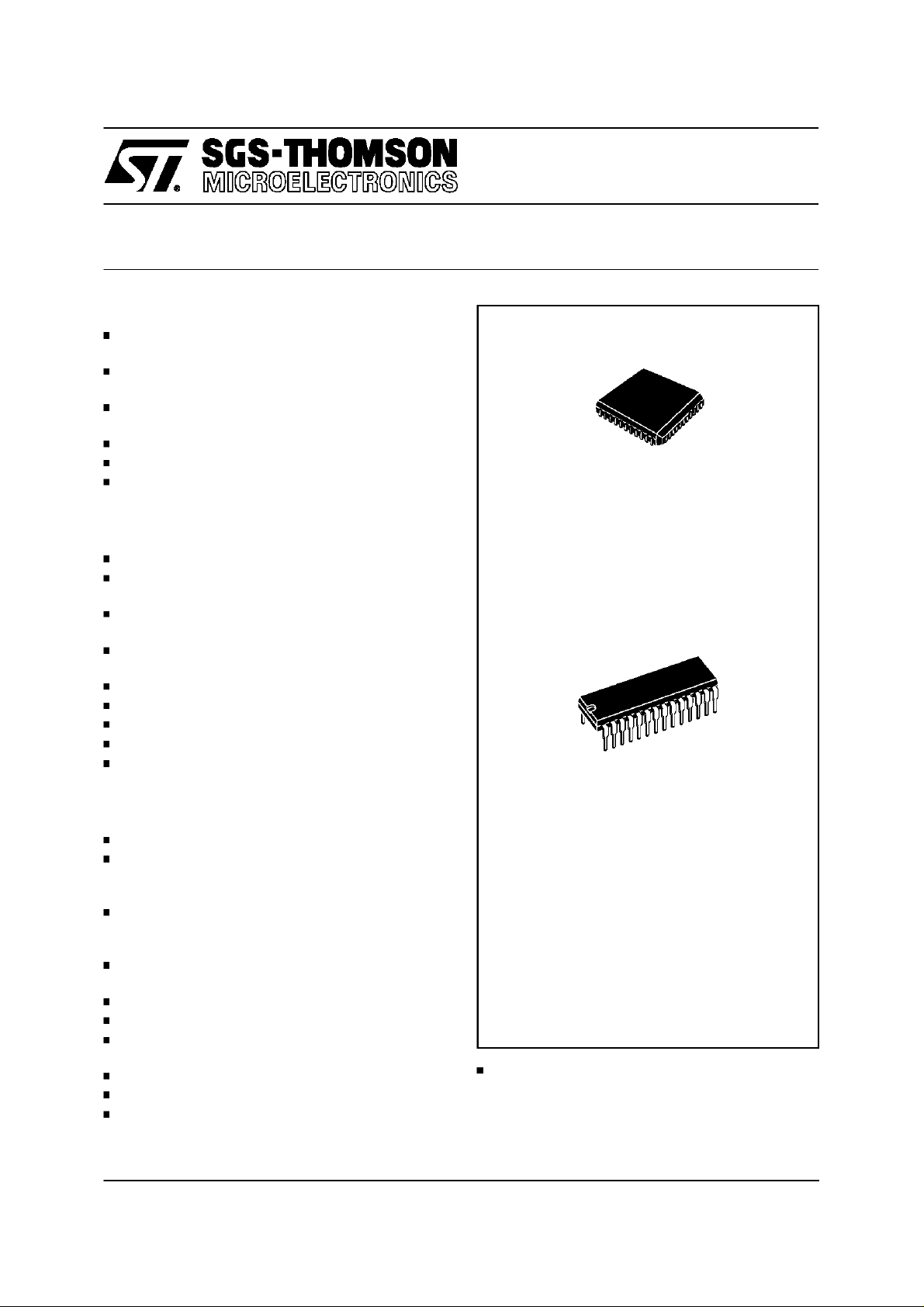
DIP28AND PLCC44 PACKAGE
HCMOS3A SGS-THOMSON ADVANCED
1.2µm DOUBLE-METALCMOS PROCESS
STLC5411
2B1Q U INTERFACE DEVICE
PLCC44
TRANSMISSION FEATURES
160 KBIT/S FULLDUPLEX TRANSCEIVER
2B1Q LINE CODING WITH SCRAMBLER/DE-
SCRAMBLER
18KFT (5.5KM) ON 26AWG/24AWG
TWISTED PAIR CABLES
SUPPORTS BRIDGE TAPS, SPLICES AND
MIXED GAUGES
>70DBADAPTIVEECHO-CANCELLATION
ONCHIP HYBRIDCIRCUIT
DECISIONFEEDBACKEQUALIZATION
ONCHIP ANALOG VCOSYSTEM
DIRECT CONNECTION TO SMALL LINE
TRANSFORMER
SYSTEMFEATURES
ACTIVATION/DEACTIVATIONCONTROLLER
ON CHIP CRC CALCULATION AND VERIFI-
CATION INCLUDING TWO PROGRAMMABLE BLOCK ERRORCOUNTERS
EOC CHANNEL AND OVERHEAD-BITS
TRANSMISSION WITH AUTOMATIC MESSAGECHECKING
GCI AND MW/DSI MODULE INTERFACES
COMPATIBLE
DIGITAL LOOPBACKS
COMPLETE(2B+ D )ANALOGLOOPBACKINLT
ELASTIC DATA BUFFERS AND BACKPLANE
CLOCKDE-JITTERIZER
AUTOMODE NT1 AND REPEATER
”U ACTIVATIONONLY” IN NT1
IDENTIFICATION CODE AS PER GCI
STANDARD
ORDERING NUMBER: STLC5411FN
Plastic DIP28
ORDERING NUMBER: STLC5411P
EASILY INTERFACEABLE WITH ST5451
(HDLC & GCI CONTROLLER), ST5421 SIDGCI TRANSCEIVER AND ANY OTHER GCI,
IDL or TDMCOMPATIBLEDEVICES
November 1996
1/72
Page 2

STLC5411
INDEX
DISTINCTIVECHARACTERISTICS .......................................... Page 1
GENERALDESCRIPTION ....................................................... 5
PIN FUNCTION ................................................................ 6
FUNCTIONAL DESCRIPTION.................................................... 14
Digital Interfaces . . . . .....................................................
µW/DSI mode . . . . . . . . . . . . . . . . . . . . . . . . . . . . . . . . . . . . . . . . ...................
µW Control Interface. . . . . . . . . . . . . . . . . . . . . . . ...............................
WriteCycle . . . . . . . . ..............................................
ReadCycle.........................................................1414
Digital System Interface. . . . . . . . . . . . . . . . ...................................
GCImode............................................................1518
Frame structure. . . . . ..............................................
Physicallinks . . . . . . . . . . . . . . . . . . . . . . . . . . . . . . . . . . . . . . . .. . . . . . . .. . . . .
Monitorchannel . . .................................................
C/I channel.. . . ...................................................
Line coding and frame format. . . . . . . . . . . . . . . . . .. . . . . . . . ....................
Transmitsection. . . . . . . . . . . . .............................................
Receivesection..........................................................
Elasticbuffers............................................................
Maintenancefunctions.. . . . . . . . . . . ........................................ 25
M channel.. . . . . . . . . . . . . . . . . . ....................................
EOC.............................................................
M4channel.......................................................
SpareM5andM6bits...............................................
CRC calculation checking. . . . . . . . . ................................. .
Loopbacks. . . . . . . . . . . . . . . . . . . . ..................................
Identificationcode. . .....................................................
GeneralpurposeI/Os......................................................
Testfunctions............................................................
14
14
14
18
18
22
23
24
24
24
25
25
25
25
26
26
26
33
33
34
Turningonandoffthedevice................................................
Poweron initialization. ...................................... ......
Line activationrequest. . . . . . . . . . . . . . . . . . . . . ........................
Powerup control. . . . . . . . . . . . . . . . . . . . . . . . . . . . . . . . . . . . ........ ....
Powerdown control . . . . . . . . . . . . . . ................................
Powerup state. . . . . . . . . . . . . . . . . . . ......................... ......
Powerdown state . . . . . . . . . . . ......................... .............
Activationdeactivationsequencing.. . . . . . . . . . . . . . . ...........................
Case of restricted activation. . . . . . .........................................
Resetof activation / deactivationstate machine . . . . . . . . . . . . . . . . . . . . . . . . . . . .. . . .. .
Hardwarereset...........................................................
Quietmode..............................................................
Automode...............................................................
34
34
34
34
35
35
35
35
35
35
35
35
36
Command/Indication(C/I) codes.. . . . . . . . . . . . . . . . . . . . . . . . ...................
Internalregister description . . . . . . ............... ...........................3640
Line interface circuit . . . . . . ...............................................
Boardlayout . . . . . . . . . . . ................................................5353
APPENDIX A: STATE MATRIX ................................................... 58
APPENDIX B: ELECTRICAL PARAMETERS ........................................ 60
2/72
Page 3
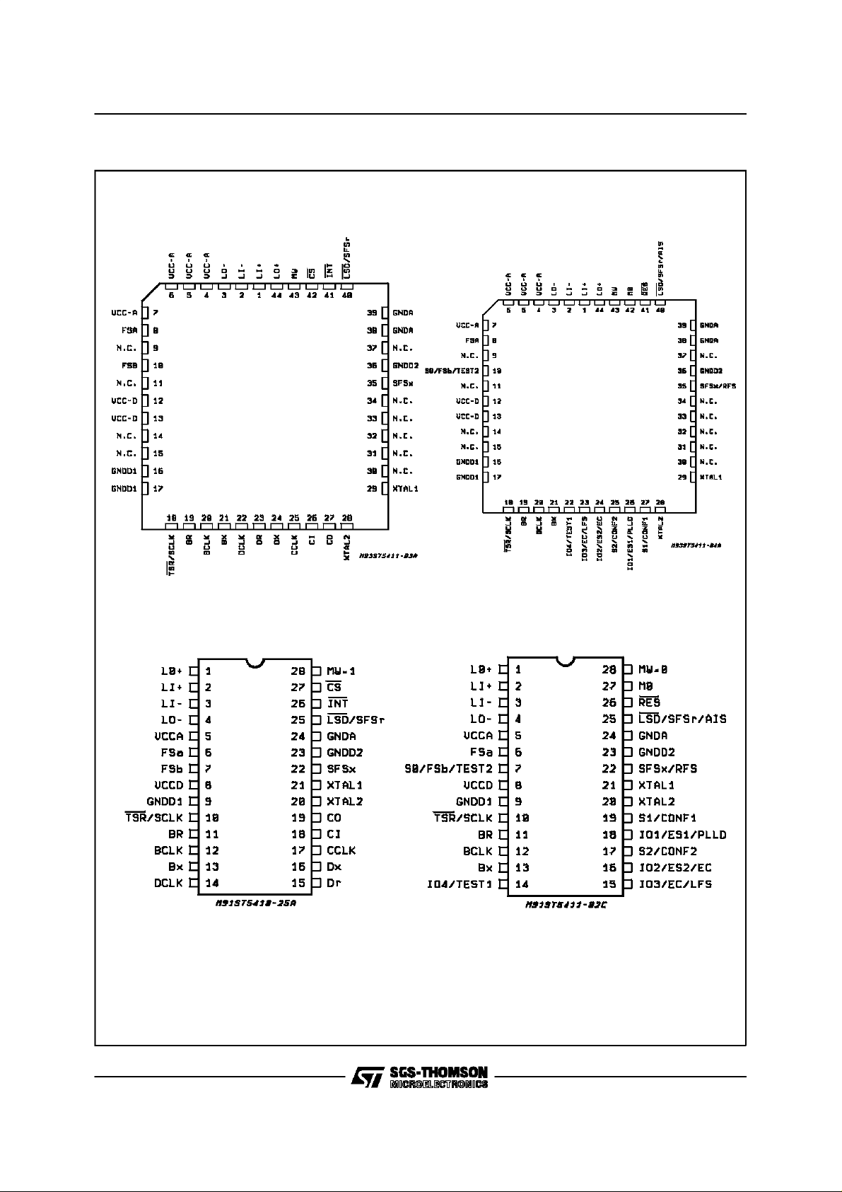
PIN CONNECTIONS (Top view)
STLC5411
PLCC44
MICROWIRE MODE
DIP28
PLCC44
GCI MODE
DIP28
MICROWIRE MODE
GCI MODE
3/72
Page 4
STLC5411
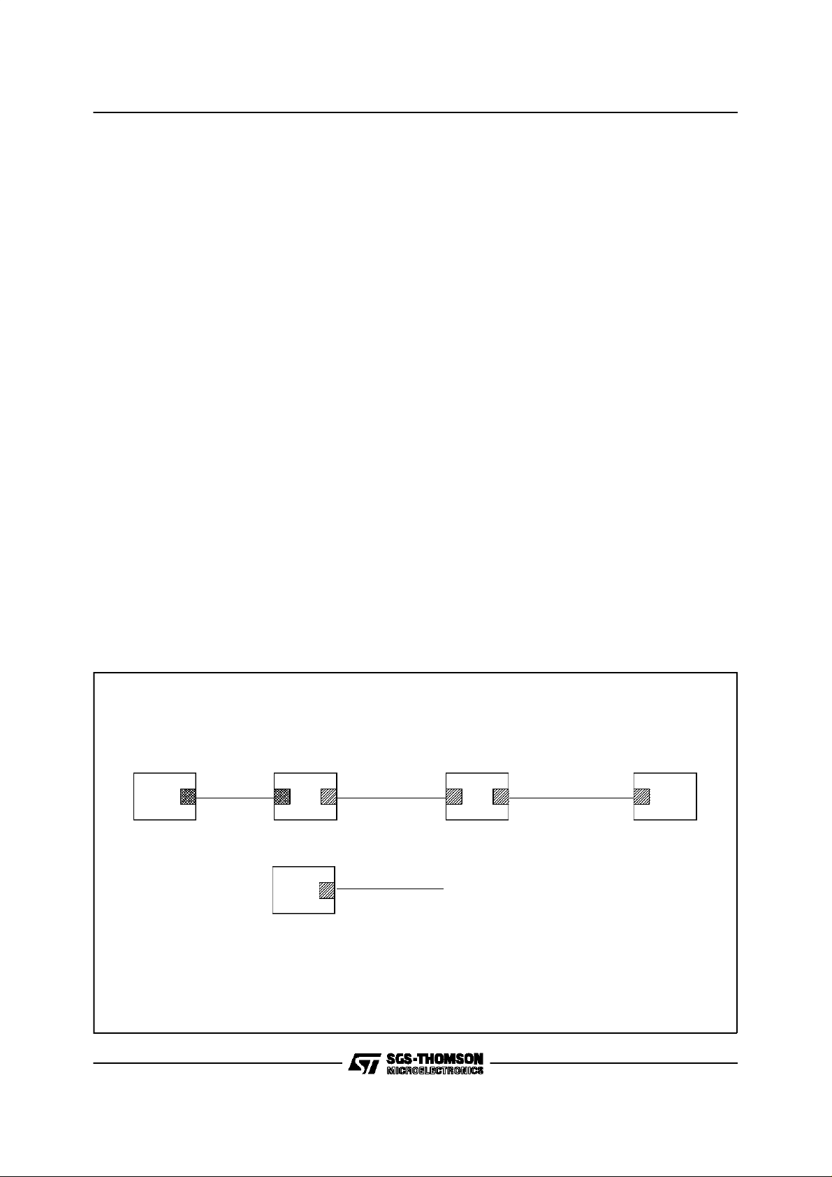
Figure1: BlockDiagram.
4/72
Page 5

STLC5411
GENERALDESCRIPTION
STLC5411 is a complete monolithic transceiver
for ISDN Basic access data transmission on
twisted pair subscriber loops typical of public
switched telephone networks. The device is fully
compatiblewith both ANSI T1.601-1988U.S. and
CSE (C32-11) French specifications. It is intended also to comply with ETSI specification
bothin term of transmissionperformances and requested features.
The equivalent of 160 kbit/s full-duplex transmission on a single twisted pair is provided, according to the formats defined in the a.m. spec.
Framesinclude two B channels,each of 64 kbit/s,
one D channel of 16 kbit/s plus an additional 4
kbit/s M channel for loop maintenance and other
user functions. 12 kbit/s bandwidthis reserved for
framing.2B1Q Line codingis used, wherepairs of
bits are coded into one of 4 quantumlevels. This
technique results in a low frequency spectrum
(160 kbit/s turn into 80 kband), thereby reducing
both line attenuation and crosstalk and achieving
long range with low Bit ErrorRates.
The system is designed to operate on standard
types of cable pairs including mixed gauges (26
AWG, 24 AWG and 22 AWG) including the 15
loops configuration specified by ANSI. Good
noise margins are achieved even when bridged
taps are present. On 26 AWG cable, the transmission range is in excess of 5.5 km (18 kft) in
presence of crosstalk and noise as specified by
ANSI standard.STLC5411 is designed to operate
with Bit Error Rate near-end Crosstalk (NEXT) as
specifiedin europeanETSI recommendation.
To meet these very demanding specifications, the
device includes two Digital Signal Processors,
one configured as an adaptive Echo-Canceller to
cancel the near end echoes resulting from the
transmit/receive hybrid interface, the other as an
adaptive line equalizer. A Digital Phase-Locked
Loop (DPLL) timing recovery circuit is also included that provides in NT modes a 15.36 MHz
synchronized clock to the rest of the system.
Scrambling and descrambling are performed as
specifiedin the US and Frenchspecifications.
On the system side, STLC5411 can be linked to
twobus configuration simply by pin MW bias.
MICROWIRE(µW/DSI) mode (MWpin = 5V): 144
kbit/s 2B+D basic access data is transferred on a
multiplex Digital System Interface with 4 different
interface formats (see fig. 2 and 3) providing
maximum flexibility with a limited pin count
(BCLK, Bx, Br, FSa, FSb). Three pre-defined
2B+D formats plus an internal time slot assigner
allows direct connection of the UID to the most
common multiplexed digital interfaces (TDM/IDL).
Bit and Frame Synchronisation signals are inputs
or outputs depending on the configuration se-
lected. Data buffers allow any phase betweenthe
line and the digital interface. That permits building
of slave-slave configurations e.g. in NT12 trunkcards.
It is possible to separate the D from the B channels and to transfer it on a separate digital interface (Dx, Dr) using the same bit and frame clocks
as for the B channelsor in a continuousmode using an internallygenerated 16 kHz bit clock output
(DCLK).
All the Control, Status and Interrupt registers are
handled via a controlchannel on a separate serial
interface MICROWIRE compatible (CI, CO, CS,
CCLK, INT) supported by a number of microcontroller including the MCU families from SGSTHOMSON
GCI mode (MWpin = 0V). Control/maintenance
channels are multiplexedwith 2B+D basic access
data in a GCI compatibleinterface format (see fig.
4a) requiring only 4 pins (BCLK, Bx, Br, FSa). On
chip GCI channel assignementallows to multiplex
on thesame bus up to 8 GCI channels,each supporting data and controls of one device. Bit and
Frame Synchronisation signals can be inputs or
ouputs depending on the configuration selected.
Data buffers, again, allow to have any phase between the lineinterface and the digitalinterface.
Through the M channel and its protocol allowing
to check both direction exchanges, internal registers can be configured, the EOC channel and the
Overhead-bits can be monitored. Associated to
the M channel, there are A and E channels for
enabling the exchanged messages and to check
the flow control. The C/I channel allows the primitive exchangesfollowing the standard protocol.
In both mode (µW and GCI) CRC is calculated
and checkedin both directions internally.
In LT mode, the transmit superframe can be synchronized by an external signal (SFSx) or be self
running. In NT mode, the SFSx is always output
synchronizedby the transmitsuperframe.
Line side or Digital Interface side loopbacks can
be selected for each B1, B2 or D channel independently without restriction in transparent or in
non-transparent mode. A transparent complete
analog loopback allowing the test of the transmission path is also selectable.
Activation and deactivationprocedures,which are
automatically processed by UID, require only the
exchange of simple commands as Activation Request, Deactivation Request, Activation Indication. Cold and Warm start up proceduresare operated automatically without any special
instruction.
Four programmable I/Os are provided in GCI for
externaldevice control.
5/72
Page 6

STLC5411
PIN FUNCTIONS (no SpecificMicrowire / GCIMode)
Note: all pin number are referred to PlasticDIP28 package.
Pin Name In/Out Description
1, 4 LO+, LO- Out, Out Transmit 2B1Q signaldifferential outputs to theline transformer. When
2, 3 LI+, LI- In, In Receive 2B1Q signal differential inputs from the line transformer.
5, 8 VCCA, VCCD In, In Positive power supply input for the analog and digital sections, which must
24,923GNDA,GNDD1
GNDD2
10 TSRb Out (LT configuration only)
SCLK Out (NT configuration only)
20 XTAL2 Out The output of the crystal oscillator, which should be connected to one end
21 XTAL1 In The master clock input, which requires either a parallel resonance crystal to
28 MW In MICROWIRE selection: When set high, MICROWIRE control interface is
In, In
In
used with an appropriate 1:1.5 step-up transformer and the proper line
interface circuit the linesignal conforms to the output specifications in ANSI
standard with anominal pulse amplitude of 2.5 Volts.
be +5 Volts +/-5% and must be directlyconnected together.
Negative power supply pins, which must be connected together close to
the device.
All digitaland analog signals are referred to these pins, whichare normally
at the system Ground.
This pin is an open drainoutput normally in the high impedance state which
pulls low when B1 and B2 time-slots are active. It can be used to enable the
Tristate control of a backplane line-driver.
15.36 MHz clock output which is frequency locked to the received line
signal activeas soon as UID is powered up except in NT1 Auto
configuration (active only if S line activation is requested)
of the crystal, if used. Otherwise, this pin must be left not connected.
be tied between this pin and XTAL2, or a logic level clock input from a
stable source. This clock does not need tobe synchronized to the digital
interface clocks (FSa, BCLK).Crystal specifications: 15.36 MHz +/-50ppm
parallel resonant; Rs ≤ 20 ohms; load with 33pF to GND each side.
selected. When set low, GCI interface is selected.
PIN FUNCTIONS (specific Micro Wire mode)
Pin Name In/Out Description
6 FSa In Out Input or Outputdepending of the CMS bitin CR1 register, FSa is a 8 KHz
7 FSb In Out Input or Outputdepending of the CMS bitin CR1 register, FSb is a 8 KHz
11 Br Out 2B+D datas tristate output. Datas received from the line are shifted out on
6/72
clock which indicates the start of the frame on Bx when FSa is input, or Bx
and Br when FSa is output.
Input or Output,the location of FSa relative to the frame on Bx orBx and Br
depens of DDM bit in CR1 register, also the selected format.
clock which indicates the start of the frame on Br when it is an input. When
it is an output, FSb is a 8 KHz pulse conforming with the selected format
and always indicatingthe second 64Kbit/sec channel of the frame on Br.
Input or Output,the location of FSb relative to the frame on Br depends of
DDM bit in CR1 register, also the selected format.
the rising edge (at the BCLK frequencyor the half BCLK frequency if format
4 is selected) during the assigned time slot. Br is in high impedance state
outside the assignedtime slot and during the assigned time slot ofthe
channel if it is disabled.
When D channel portis enabled, only B1 B2 are on Br.
Page 7

STLC5411
PIN FUNCTIONS (specific Micro Wire mode)
Pin Name In/Out Description
12 BCLK In Out Bit clock input or output depending of the CMS bit in CMR register. When
13 Bx In 2B+D input. Basic access data to transmit to the line is shifted in on the
14 DCLK Out D channel clock output when the D channel port is enabled in continuous
15 Dr Out D channel data output when theD channel portis enabled. D channel data is
16 Dx In D channel data inputwhen the D channel port is enabled. D channel data is
17 CCLK In ClockinputfortheMICROWIREcontrolchannel: data is shiftedin and outon
18 CI In MICROWIRE control channel serial input: Two bytes data is shifted out the
19 CO Out MICROWIRE control channel: serial output: two bytes data is shifted out the
22 SFSx In Out Tx Super frame synchronization. The rising edgeof SFSxindicates the
25 SFSr Out Rx Super frame synchronization. The rising edge of SFSr indicates the
LSDb Out Line Signal Detect output (default conf.): This pin is an open drain output
26 INTb Out Interrupt output: Latched open-drain output signal which isnormally high
27 CS In Chip Select input: When this pin is pulled low, data can be shifted in and out
BCLK is an input, its frequency may be any multiple of 8 KHz from 256 KHz
to 4096 KHz in formats 1, 2, 3; 512 KHz to 6176 KHz in format 4. When
BCLK is an output, its frequency is 256 KHz, 512 KHz, 1536 KHz, 2048
KHz or 2560 KHz depending of the selection in CR1 register. In this case,
BCLK is locked to the recovered clock received from the line. Input or
Output BCLK is synchronous with FSa/FSb. Datas are shifted in and out (on
Bx and Br) at the BCLK frequency in formats1, 2, 3. In format 4 datas are
shifted out at half the BCLK frequency.
falling edges (at the BCLK frequency or the half BCLK frequency if format 4
is selected) during the assigned time-slots. When D channel port is
enabled, only B1 & B2 sampled on Bx.
mode. Datas are shifted in and out (on Dx and Dr) at 16 KHz on the falling
and rising edges of DCLK respectively. In master mode, DCLK is
synchronous with BCLK.
shifted out from the UID on thispinin 2 selectable modes: in TDM mode data
is shiftedout at the BCLKfrequency (orhalf BCLK frequency in format4) on
theridsing edgeswhentheassigned timeslot is active.In continuousmode
dataisshiftedout attheDCLK frequency on the risingedge continuously.
shifted infrom the UID on this pin in 2 selectable modes: in TDM mode data
is shifted in at the BCLK frequency (or half BCLK frequency in format 4) on
the falling edges when the assigned time slot is active. In continuous mode
data is shiftedout at the DCLK frequency on the fallingedge continuously.
CI and CO pins withCCLK frequency following2 modes. For each modethe
CCLKpolarity is indifferent. CCLK may be asynchronous with all the others
UID clocks.
UID on this pin on the rising or the falling edge of CCLK depending of the
working mode.
UID on this pin on the rising or the falling edge of CCLK depending of the
working mode. When not enabled by CS low, CO is high impedance.
beginning of thetransmit superframe on theline. In NT mode SFSxis always
an output. In LT mode SFSx is an input or an output depending of the SFSbit
in CR2 register. When SFSx is input,it must be synchronous of FSa.
begenning of the received superframe on the line. UID provides this output
only when ESFR bit in CR4 register is to 1.
which is normally in the high impedance state but pulls low when the device
previously in the power down state receives a wake-up by Tone from the
line. This signal is intended to be used to wake-up a micro-controller from a
low power idlemode. The LSD output goes back in the high impedance
state when the device is powered up.
impedance and goes low to request a read cycle. Pending interrupt datais
shiftedout from CO at thefollowing read-write cycle. Several pending interrupts
maybequeuedinternally and may provide severalinterrupt requests. INTis
freed uponreceiving ofCS lowandcan goes lowagain when CS is freed.
from the UID through CI & CO pins. When high, this pin inhibits the
MICROWIRE interface. For normal read or write operation, CS has to be
pulled low for 16 CCLK periods of time.
7/72
Page 8

STLC5411
PIN FUNCTIONS (specific GCI mode)
Pin Name In/Out Description
6 FSa In Out Input or Outputdepending of the configuration. FSa is a 8 KHz clock which
7 FSb Out In NT/TE non auto-mode configuration, FSb is a 8 KHz pulse always
S0 In When MO = 0 (LT/NT12 configuration): S0 associated with S1 and S2
TEST2 In Input pin to select a transmission test in all auto mode configurations.
11 Br Out 2B+D and GCI control channel open drain output. Data is shifted out (at the
12 BCLK In Out Bit clock input or output depending of the configuration. When BCLK is an
13 Bx In 2B+D and GCI control channelinput. Data is sampled by the UID on the
14 IO4 In Out General purpose programmable I/O configured by CR5 register in all non
TEST1 In Input pin to select a transmission test in all auto mode configurations.
15 IO3 In Out General purpose programmable I/O configured by CR5 register in all non
EC Out External control output pin in NT1 auto configuration. Normaly high, this pin
LFS In Local febe select:
16 IO2 In, Out General purpose programmable I/O configured by CR5 register in all non
EC Out External control output pin in LTRR auto configuration. Normaly high, this
ES2 In External status input pin. In NT1 autoand NTRR auto configurations, this
17 S2 In When MO = 0 (LT/NT12 configuration): S2 associated with S0 and S1
CONF2 In When MO = 1: Configuration input pin. Is used associated with CONF1 to
18 IO1 In Out General purpose programmable I/O configured by CR5 register in all non
ES1 In External status input pin. In NT1 autoand NTRR auto configurations, this
PLLD In PLL1 can be disabled in LTRR onto configuration with this pin.
19 S1 In When MO = 0 (LT/NT12 configuration): S1 associated with S0 and S2
CONF1 In When MO = 1: Configuration input pin. Is used associated with CONF2 to
indicates the start of the frame onBx and Br.
indicating the second 64Kbit/sec channel of the frame on Br.
selects a GCI channel number on Bx/Br.
TEST2 is associated with TEST1.
half BCLK frequency) on the first rising edge of BCLK during the assigned
channels slot. Br is in highimpedance state outside the assigned time slot
and during the assigned time slot of a channel if it is disabled.
input, its frequency may be any multiple of 16 KHz from 512 KHz to 6176
KHz.. When BCLK is an output, its frequence is 512 KHz in NT1 auto and
NTRR auto configurations, 1536 KHz in NT/TE configuration; In this case,
BCLK is locked to the recovered clock received from the line. Input or
Output BCLK is synchronous with FSa. Datas are shifted in and out (on Bx
and Br) at the half the BCLK frequency.
second falling edge of BCLK within the period of the bit, during the assigned
channels time slot.
auto mode configurations.
TEST1 is associated with TEST2.
auto mode configurations.
is pulled low when an eoc message ”öperate 2B+D loopback” is recognized
from the line.
When tied to 1 the febe is locallylooped back. See figure 10.
auto mode configurations.
pin is pulled low when an ARL command is received by the UID.
status is sent on the line throughthe ps2 bit.
selects a GCI channel number on Bx/Br.
select configuration NT/TE (non auto), NT1 auto, LTRR auto and NTRR
auto.
auto mode configurations.
status is sent on the line throughthe ps1 bit.
selects a GCI channel number on Bx/Br.
select configuration NT/TE (non auto), NT1 auto, LTRR auto and NTRR
auto.
8/72
Page 9

STLC5411
PIN FUNCTIONS (specific GCI mode)
Pin Name In/Out Description
22 RFS In Remote febe select:
25 AIS In Analog interface select for all auto mode configurations
SFSr Out Rx Super frame synchronization. The rising edge of SFSr indicates the
LSDb Out Line Signal Detect output (default conf.): This pin is an open drain output
26 RESb In Reset input pin with internal pull-up resistor. When pulled low, all registers
27 M0 In Configuration input pin. When pulled low, GCI channel assigner is selected
When tied to 0 the remote febe is not transferred. When tied to 1 febe is
transparently reported. Seefigure 10.
beginning of the received superframe on the line. UID provides this output
only when ESFR bit in CR4 register is to 1 and LT/NT12 or NT/TE
configuration is done.
which is normally in the high impedance state but pulls low when the device
previously in the power down state receives a wake-up by Tone from the
line. This signal is intended to be used to wake-up a micro-controller from a
low power idlemode. The LSD output goes back in the high impedance
state when the device is powered up.
of the UID are reset to their default values. UID is configuredaccording to
configuration inputs bias excluding MW input which must be maintained at
the 0 volt. minimum recommended pulse length is 200µs.
(channel number defined by inputs S0, S1, S2). When pulled high, UID is
configured by pins CONF1 and CONF2.
MULTIPLE FUNCTION PIN DESCRIPTION
Pin6: FSa
Function or In/Out conditions (*) Function In/Out
MW(pin) = 1
MW(pin) = 0
MO(pin) = 1
MO(pin) = 0 FSa In
CMS(cr1) = 1 FSa Out
CMS(cr1) = 0 FSa In
CONF2(pin) = 1
CONF2(pin) = 0
(*) Only true if ANATST (internal test signal) = 0
CONF1(pin) = 1 FSa Out
CONF1(pin) = 0 FSa Out
CONF1(pin) = 1 FSa In
CONF1(pin) = 0 FSa Out
9/72
Page 10
STLC5411
MULTIPLE FUNCTION PIN DESCRIPTION
Pin7: S0/FSb/TEST2
Function or In/Out conditions (*) Function In/Out
MW(pin) = 1
MW(pin) = 0
MO(pin) = 1
MO(pin) = 0 S0 In
(*) Only true if ANATST (internal test signal) = 0
Pin10: TSR~/SCLK/TCLK
Function or In/Out conditions (*) Function In/Out
MW(pin) = 1
MO(pin) = 1
MW(pin) = 0
MO(pin) = 0
(*) Only true if TDSPANA (internal testsignal) = 0
CMS(cr1) = 1 FSb Out
CMS(cr1) = 0 FSb In
CONF2(pin) = 1
CONF2(pin) = 0
NTS(cr2) = 1 SCLK Out
NTS(cr2) = 0 TSR~ Out OD
CONF2(pin) = 1
CONF2(pin) = 0
NTS(cr2) = 1 SCLK Out
NTS(cr2) = 0 TSR~ Out OD
CONF1(pin) = 1 TEST2 In
CONF1(pin) = 0 FSb Out
CONF1(pin) = 1 TEST2 In
CONF1(pin) = 0 TEST2 Out
CONF1(pin) = 1 SCLK Out
CONF1(pin) = 0 SCLK Out
CONF1(pin) = 1 TSR~ Out OD
CONF1(pin) = 0 SCLK Out
Pin12: BCLK
MW(pin) = 1
MW(pin) = 0
10/72
Function or In/Out conditions Function In/Out
CMS(cr1) = 1 BCLK Out
CMS(cr1) = 0 BCLK In
CONF2(pin) = 1
MO(pin) = 1
CONF2(pin) = 0
MO(pin) = 0 BCLK In
CONF1(pin) = 1 BCLK Out
CONF1(pin) = 0 BCLK Out
CONF1(pin) = 1 BCLK In
CONF1(pin) = 0 BCLK Out
Page 11
MULTIPLE FUNCTION PIN DESCRIPTION
Pin14: DCLK/IO4/TEST1/TSYNC[R+]
Function or In/Out conditions Function In/Out
MW(pin) = 1
MO(pin) = 1
MW(pin) = 0
MO(pin) = 0
DEN(cr2) = 1
DEN(cr2) = 0 TSYNC Out
CONF2(pin) = 1
CONF2(pin) = 0 TEST1 In
Pin15: Dr/IO3/EC/LFS/TDOUT[R+]
Function or In/Out conditions (*) Function In/Out
MW(pin) = 1
MO(pin) = 1
MW(pin) = 0
MO(pin) = 0
DEN(cr2) = 1 Dr Out
DEN(cr2) = 0 TDOUT Out
CONF2(pin) = 1
CONF2(pin) = 0 LFS In
(*) Only true if TDSPANA (internal testsignal) = 0
STLC5411
DMO(cr2) = 1 DCLK Out
DMO(cr2) = 0 TSYNC Out
CONF1(pin) = 1 TEST1 In
CONF1(pin) = 0
CONF1(pin) = 1 EC Out
CONF1(pin) = 0
IO4(cr5) = 1 I4 In
IO4(cr5) = 0 O4 Out
IO4(cr5) = 1 I4 In
IO4(cr5) = 0 O4 Out
IO3(cr5) = 1 I3 In
IO3(cr5) = 0 O3 Out
IO3(cr5) = 1 I3 In
IO3(cr5) = 0 O3 Out
Pin16: Dx/IO2/EC/ES2/TDIN[R+]
Function or In/Out conditions (*) Function In/Out
MW(pin) = 1
MO(pin) = 1
MW(pin) = 0
MO(pin) = 0
DEN(cr2) = 1 Dx In
DEN(cr2) = 0 TDIN In
CONF2(pin) = 1
CONF2(pin) = 0
(*) Only true if TGSCEN(internal test signal) = 0
CONF1(pin) = 1 ES2 In
CONF1(pin) = 0
CONF1(pin) = 1 EC Out
CONF1(pin) = 0 ES2 In
IO2(cr5) = 1 I2 In
IO2(cr5) = 0 O2 Out
IO2(cr5) = 1 I2 In
IO2(cr5) = 0 O2 Out
11/72
Page 12

STLC5411
MULTIPLE FUNCTION PIN DESCRIPTION
Pin17: CCLK/S2/CONF2
Function or In/Out conditions Function In/Out
MW(pin) = 1 CCLK In
MW(pin) = 0
Pin18: CI/IO1/ES1/PLLD[R+]
MW(pin) = 1 CI In
MW(pin) = 0
Pin19: CO/S1/CONF1
MO(pin) = 1 CONF2 In
MO(pin) = 0 S2 In
Function or In/Out conditions Function In/Out
CONF1(pin) = 1 ES In
MO(pin) = 1
MO(pin) = 0
CONF2(pin) = 1
CONF2(pin) = 0
CONF1(pin) = 0
CONF1(pin) = 1 PLLD In
CONF1(pin) = 0 ES1 In
IO1(cr5) = 1 I1 In
IO1(cr5) = 0 O1 Out
IO1(cr5) = 1 I1 In
IO1(cr5) = 0 O1 Out
Function or In/Out conditions Function In/Out
MW(pin) = 1 CO Out
MW(pin) = 0
MO(pin) = 1 CONF1 In
MO(pin) = 0 S2 In
Pin22: SFSx/RFS [R+]
Function or In/Out conditions Function In/Out
NTS(cr2) = 1 SFSx Out
MW(pin) = 1
MW(pin) = 0
MO(pin) = 1
MO(pin) = 0
NTS(cr2) = 0
CONF2(pin) = 1 SFSx Out
CONF2(pin) = 0 RFS In
NTS(cr2) = 1 SFSx Out
NTS(cr2) = 0
SFS(cr2) = 1 SFSx Out
SFS(cr2) = 0 SFSx In
SFS(cr2) = 1 SFSx Out
SFS(cr2) = 0 SFSx In
12/72
Page 13
STLC5411
MULTIPLE FUNCTION PIN DESCRIPTION
Pin25: LSD/SFSr/AIS
Function or In/Out conditions Function In/Out
MW(pin) = 1
CONF1(pin) = 1 AIS In
MO(pin) = 1
MW(pin) = 0
MO(pin) = 0
CONF2(pin) = 1
CONF2(pin) = 0 AIS In
CONF1(pin) = 0
Pin26: INT/RES [R+]
Function or In/Out conditions Function In/Out
MW(pin) = 1 INT Out OD
MW(pin) = 0 MO In
ESFR(cr4) = 1 SFSr Out OD
ESFR(cr4) = 0 LSD Out OD
ESFR(cr4) = 1 SFSr Out OD
ESFR(cr4) = 0 LSD Out OD
ESFR(cr4) = 1 SFSr Out OD
ESFR(cr4) = 0 LSD Out OD
Pin27: CS/MO
Function or In/Out conditions Function In/Out
MW(pin) = 1 CS In
MW(pin) = 0 MO In
PIN28: MW
Notes: [R+] = Pull up Resistor
: Out OD = Open Drain Output
13/72
Page 14

STLC5411
FUNCTIONAL DESCRIPTION
DigitalInterfaces
STLC5411 provides a choice between two types
of digital interface for both control data and (2
B+D) basic accessdata.
Theseare:
a) GeneralCircuit Interface:GCI.
b) Microwire/DigitalSystem Interface:
µW/DSI
The device will automatically switch to one of
them by sensing the MW input pin at the Power
up.
µW/DSI MODE
Microwirecontrol interface
The MICROWIRE interface is enabled when pin
MW equal one. Internalregisters can be writtenor
readthrough that controlinterface.
It is constitutedof 5 pins:
CI:
CO:
CCLK:
CS:
INT:
data in
data output
data clock input
Chip Select input
Interruptoutput
Transmission of data onto CI & CO is enabled
when CS input is low.
A Write cycle or a Read cycle is always constituted of two bytes. CCLK must be pulsed 16
times while CS is low.
Transmission of data onto CI & CO is enabled following2 modes.
– MODE A: the first CCLK edge after CS fall-
ing edge (and fifteen others odd CCLK
edges) are used to shift in the CI data, the
even edges being used to shift out the CO
data.
– MODEB: the CCLK first edge after CS falling
edge (and the fifteen others odd CCLK loss)
are used to shift out the CO data, the even
edges being used to shift in the CI data.
Foreach modes the first CCLK edge after CS falling edge can be positive or negative: the UID
automaticalydetects the CCLKpolarity.
Mode A is the default value. To select the mode
B, write MWPS register.
Youcan writein the UID on CI whilethe UID send
back a register content to the microprocessor. If
the UID has no messageto send, it forces the CO
output to all zero’s.
If the UID is to be read (status change has occured in the UID or a read-back cycle has been
requested by the controller), it pulls the INT output low until CS is provided. INT high to low
transition is not allowed when CS is low (the UID
waits for CS high if a pending interrupt occurs
14/72
while CS islow) .
When CS is high, the CO pin is in the high imped-
ance state.
Write cycle
The format to write a 8 bits message into the UID
is:
A7 A6 A5 A4 A3 A2 A1 A0
1st byte
D7 D6 D5 D4 D3 D2 D1 D0
2nd byte
A7-A1:
A0:
D7-D0:
Register Address
Write/Readback Indicator
Register Content
After the first byte is shifted in, Register address
is decoded. A0 set low indicates a write cycle: the
content of the following received byte has to be
loaded into the adressed register.
A0 set high indicates a read-back cycle request
and the byte following is not significant. The UID
will respond to the request with an interrupt cycle.
It is then possible for the microprocessor to receive the required register content after several
other pending interrupts.
To writea 12bits message,the differenceis:
limited addressfield: A7- A4
extended data field (D11 - D8): A3 - A0.
The Write/Read back indicator doesn’t apply; to
read and write a 12 bits register two addresses
are necessary.
Read cycle
When UID has a register content to send to the
microprocessor, it pulls low the INT output to request CS and CCLK signals.Note that the data to
send can be the content of a Register previously
requested by the microprocessor by means of a
read-back request.
The formatof the 8 bits message sent by the UID
is:
A7 A6 A5 A4 A3 A2 A1 A0
1st byte
D7 D6 D5 D4 D3 D2 D1 D0
2nd byte
A7-A1:
A0:
RegisterAddress
forced to 1 if read back
forced to 0 if spontaneous
D7-D0:
RegisterContent
Page 15

STLC5411
To read a 12 bitsmessage, the difference is:
limitedaddress field: A7 - A4
extendeddata field (D11- D8):A3 - A0.
The Write/Read back indicator doesn‘t exit.
DIGITALSYSTEM INTERFACE
TwoB channels,eachat 64 kbit/sandone D channel at 16 kbit/s form the Basic access data. Basic
accessdata is transferredon the DigitalSystemInterface with several different formats selectable by
meansof the configurationregister CR1.
The DSI is basically constituted of 5 wires (see
fig.2 and 3):
BCLK
Bx
Br
FSa
FSb
bit clock
data input to transmit to the line
data output received fromthe line
TransmitFrame sync
ReceiveFrame sync
It is possible to separate the D channelfrom the B
channels and to transfer it on a separate Digital
Interfaceconstituted of 2 pins:
Dx
Dr
D channel data input
D channel data ouput
The TDM (Time Division Multiplex) mode uses
the same bit and frame clocks as for the B channels. The continuous mode uses an internally
generated16 kHz bit clock output:
DCLK D channel clockoutput
For all formats when D channel port is enabled
”continuous mode” is possible. When the D channel port is enabled in TDM mode, D bits are assigned according to the related format on Dx and
Dr .
STLC5411 provides a choice of four multiplexed
formats for the B and D channels data as shown
in fig.2 and3.
Format 1: the 2B+D data transfer is assigned to
the first 18 bits of the frame on Br and Bx I/0 pins.
Channels are assigned as follows: B1(8 bits),
B2(8 bits), D(2 bits), with the remaining bits ignoreduntil the next Frame sync pulse.
Format 2: the 2B+D data transfer is assigned to
the first 19 bits of the frame on Br and Bx I/O
pins. Channels are assigned as follows: B1(8
bits), D(1 bit), 1 bit ignored, B2(8 bits), D(1 bit),
with the remaining bits ignored until the next
frame sync pulse.
Format 3: B1 and B2 Channels can be independently assigned to any 8 bits wide time slot
among 64 (or less) on the Bx and Br pins. The
transmit and receive directions are also independent. When TDM mode is selected, the D
channel can be assigned to any 2 bits wide time
slot among 256 on the Bx and Br pins or on the
Dx and Dr pins (D port disabled or enabled in
TDM mode respectively).
Format 4: is a GCI like format excluding Monitor
channel and C/I channel. The 2B+D data transfer
is assigned to the first 26 bits of the frame on Br
and Bx I/O pins. Channels are assigned as follows. B1(8 bits) B2(8 bits), 8 bits ignored, D(2
bits), with remaining bits ignored up to the next
frame sync pulse.
When the Digital Interface clocks are selected as
inputs, FSa must be a 8 kHz clock input which indicates the start of the frameon the data input pin
Bx. When the Digital Interface clocks are selected
as outputs, FSa is an 8 kHz output pulse conforming to the selected format which indicates
the frame beginning for both Tx and Rx directions.
When the Digital Interface clocks are selected as
inputs, FSb is a 8 kHz clock input which defines
the start of the frame on the data ouput pin Br.
When the Digital Interface clocks are selected as
outputs, FSb is a 8 kHz output pulse indicating
the second 64kbit/s slot.
Two phase-relations between the rising edge of
FSa/FSb and the first (or second for FSb as output) slot of the frame can be selected depending
on format selected: Delayed timing mode or non
Delayed timingmode.
Non delayed data mode is similar to long frame
timing on the COMBOI/II series of devices: The
first bit of the frame begins nominally coincident
with the rising edge of FSa/b. When output, FSa
is coincident with the first 8 bits wide time-slot
while FSb is coincident with the second 8 bits
wide time-slot. Non delayed mode is not available
in format2.
Delayed timing mode, which is similar to short
frame sync timing on COMBO I/II, in which the
FSa/b input must be set high at least a half cycle
of BCLK earlier the frame beginning. When output, FSa 1bit wide pulse indicates the first 8 bits
wide time-slot while FSb indicates the second.
Delayed mode is not availablein format 4.
2B+D basic access data to transmit to the line
can be shifted in at the BCLK frequency on the
falling edges during the assigned time-slots.
When D channel port is enabled, only B1 & B2
data is shiftedin duringthe assigned time slots. In
format 4, data is shifted in at half the BCLK frequency on the receive fallingedges.
2B+ D basic access data received from the line
can be shiftedout from the Broutput at the BCLK
frequencyon the rising edges during the assigned
time-slots. Elsewhere,Br isin the high impedance
state. When the D channel port is enabled, only
B1 & B2 data is shifted out from Br. In Format 4,
data is shifted out at half the BCLK frequency on
the transmit risingedges; thereis 1.5period delay
between the rising transmit edge and the receive
falling edge of BCLK.
15/72
Page 16
STLC5411
Bit Clock BCLK determines the data shift rate on
the Digital Interface. Depending on mode selected, BCLK is an input which may be any multiple of 8 kHzfrom 256 kHz to 6176 kHz or an output at a frequency depending on the format and
the frequencyselected. Possible frequenciesare:
256 KHz, 512 KHz, 1536 KHz,
Figure2: DSI Interfaceformats: MASTERmode.
2048 KHz, 2560 KHz.
In format 4 the use of 256kHz is forbidden.
BCLK is synchronous with FSa/b frame sync sig-
nal. When output, BCLK is phased locked to the
recoveredclock received from the line.
16/72
Page 17
Figure3: DSI Interfaceformats: SLAVEmode.
STLC5411
17/72
Page 18
STLC5411
GCI MODE
The GCI is a standard interface for the interconnection of dedicated ISDN components in the different equipments of the subscriber loop :
In a Terminal, GCI interlinks the STLC5411, the
ISDN layer 2 (LAPD) controller and the voice/data
processingcomponents as an audio-processoror
a TerminalAdaptormodule.
In NT1-2, PABX subscriber line card, or central
office line card (LT), GCI interlinks the UID, the
ISDN Layer 2 (LAPD) controllers and eventually
the backplane where the channels are multiplexed.
In NT1, GCI interlinks SID-GCI and STLC5411,
via automode (NT1-auto). In Regenerators, GCI
links both STLC5411 UID in automode (NT-RRauto,LT-RR-auto). (See Fig. 4a)
Frame Structure
2B+D data and control interfaceis transferred in a
time-division multiplexed mode based on 8 kHz
frame structure and assigned to four octets per
frame and direction.(see fig.4b).
The 64 kbit/s channels B1 and B2 are conveyed
in the first two octets; the third octet (M: Monitor)
is used for transferring most of the control and
status registers; the fourth octet (SC: Signalling &
Control) contains the two D channel bits, the four
C/I (command/lndicate)bits controlling the activation/deactivation procedures, and the E & A bits
which support the handling of the Monitor channel.
Figure4a: GCI configurationsof the UID.
These four octets per frame serving one ISDN
subscribers line form a GCI Channel. One GCI
channelcalls for a bit rate of 256 kbit/s.
In NT1-2s or subscriber Line Cards up to 8 GCI
channels may be carried in a frame of a GCI multiplex.The bit rate of a GCI multiplex may be from
256 kbit/s and up to 3088 kbit/s. Adjacent 4-octet
slots from the frame start are numbered 0 to 7.
The GCI channel takes the number of the slot it
occupies. Spare bits in the frame beyond 256 bits
from the frame start will be ignored by GCI compatible devices but may be used for other purposes if required (see Fig.4c). GCI channel number is selected by biasingpins S0,S1,S2.
PhysicalLinks
Four physical links are usedin the GCI.
Transmitteddata to the line:Bx
Received data from the line: Br
Data clock: BCLK
Frame Synchronizationclock: FSa
GCI is always synchronized by frame and data
clocks derivedby any masterclock source.
A device used in NT mode can deliver clock
sources able to synchronize GCI, either directly,
or via a local Clock Generator synchronized on
the line by means of the SCLK 15.36 MHz output
clock. Frame clock and data clock could be independent of the internal devices clocks. Logical
one on the Br output is the high impedance state
while logical zero is low voltage. For E and A bits,
active state is voltage Low while inactive state is
high impedancestate.
Figure 4a: GCI configurations of the UID
TERMINAL
18/72
NT1 REPETOR
NT
PRIVATE TERMINAL
OR NT1-2
U
LTNT-RR-AUTOLT-RR-AUTONT1-AUTOSID-GCISID-GCI
LINE TERMINATI ONSU U
Page 19
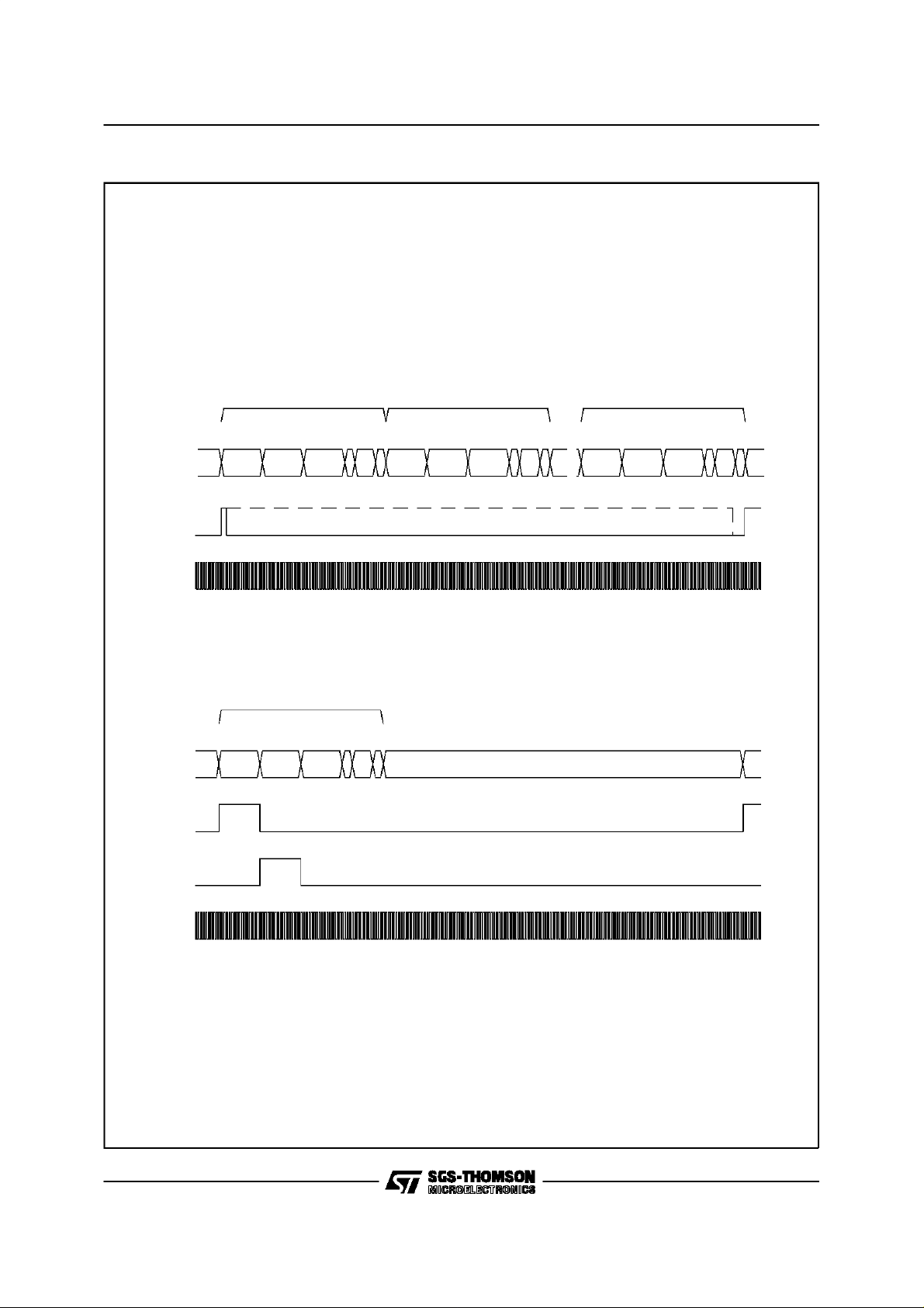
Figure4b: GCI interface format.
STLC5411
Figure 4b:
Bx/Br
FSa
BCLK
Bx/Br
GCI interface format
GCI CHANNEL 0 GCI CHANNEL 1 GCI CHANNEL 7
B1 B2 M D C/I A E
88 8242
8 KHz
GCI CHANNEL 0
B1 B2 M D C/I A E
8 8 8 242
B1 B2 M D C/I A E
8 8 8 242
SLAVE MODE
FREE
B1 B2 M D C/I A E
88 8242
FSa
FSb
BCLK
8 KHz
MASTER MODE (BCLK = 1.536MHz)
MASTERMODE
19/72
Page 20

STLC5411
Figure4c: GCI multiplex examples, (slave mode).
20/72
Page 21

STLC5411
Data is transmitted in both directions at half the
data clock rate. The information is clocked by the
transmitteron the front edge of the data clock and
can be accepted by the receiver after 1 to 1.5 period of the data clock.
The data clock (BCLK) is a square wave signal at
twice the data transmission frequency on Bx and
Br with a 1 to 1 duty cycle. The frequency can be
choosen from 512 to 6176 kHz with 16 kHz
modularity. Data transmission rate depends only
on the data clock rate.
The Frame Clock FSa is a 8 kHz signal for synchronization of data transmission.The front edge
of this signal gives the time reference of the first
bit in the first GCI input and output channel, and
reset the slot counter at thestart of each frame
When some GCI channels are not selected on
devices connected to the same GCI link, these
time slots are free for alternativeuses.
GCI configuration selection is done by biasing of
input pins MW, M0, CONF1, CONF2 accordingto
TABLE1.
Table 1: GCI Configurationselection.
Pin Number Pin name
LT/NT12* NT/TE NT1-AUTO LT-RR-AUTO NT-RR-AUTO
28MW00000
27 M0 0 1 1 1 1
19 S1/CONF1 S1 0 1 1 0
17 S2/CONF2 S2 1 1 0 0
7 S0/FSb/TEST2 S0 FSb TEST2 TEST2 TEST2
Configuration
18 IO1/ES1 IO1 IO1 ES1 PLDD ES1
16 IO2/ES2 IO2 IO2 ES2 EC ES2
15 IO3/EC IO3 IO3 EC LFS LFS
14 IO4/TEST1 IO4 IO4 TEST1 TEST1 TEST1
22 SFSx/RFS SFSx SFSx SFSx RFS RFS
* DifferentationbetweenLT and NTconfigurationdone by bit NTS inCR2 register; GCI in slavemode.
When NT1-AUTO or NT-RR-AUTO configuration is selected, BCLK bit clock frequency of 512 kHz is
automaticallyselected
WhenNT configurationis selected,BCLK bit clockfrequency of 1536 kHz is automaticallyselected.
* *Connected to V
throughinternal pull-up resistors.
CC
21/72
Page 22

STLC5411
Monitorchannel
The Monitor channel is used to write and read all
STLC5411 internal registers. Protocol on the
Monitor channel allows a bidirectional transfer of
bytes between UID and a control unit with acknowledgementat each received byte. Bytes are
transmitted on the Br output and received on the
Bx input in the Monitor channel time slot.
A write or read cycle is always constituted of two
bytes.(seefig. 5). It is possible to operate several
write or read cycles within a single monitor message.
Note: Special format is used for EOC channel.
Writecycle
The format to write a message into the UID is:
A7 A6 A5 A4 A3 A2 A1 A0
1st byte
D7 D6 D5 D4 D3 D2 D1 D0
2nd byte
A7-A1:
A0:
D7-D0:
Register Address
Write/Readback Indicator
Register Content
After the first byte is shifted in, Register address
is decoded. A0 set low indicatesa write cycle: the
content of the following received byte has to be
loadedinto the addressed register.
A0 set high indicates a read-back cycle request.
the second byte content is not significative.
STLC5411 will respond to the request by sending
back a message with the register content associated with its own address. It is then possible for
the microprocessor to receive the required register content afterseveral other pending messages.
To avoid any loss of data, it is recommended to
operateonly one read-backrequest at a time.
Note: Special format is used for EOC channel.
Readcycle
When UID has a register content to send to the
controller, it send it on the monitor channel directly. Note that the data to send can be the content of a Register previously requested by the
controllerby meansof a read-back request.
The format of the message sent by the UID is:
A7 A6 A5 A4 A3 A2 A1 A0
1st byte
D7 D6 D5 D4 D3 D2 D1 D0
2nd byte
A7-A1:
A0:
Register Address
forced to 0is spontaneous
interrupt, forced to 1 if readback
D7-D0:
Register Content
Exchange Protocol
STLC5411 validates a received byte if it is detected two consecutive times identical. (see fig. 5)
The exchangeprotocol is identical for both directions. The sender uses the E bit to indicate that it
is sending a Monitor byte while the receiver uses
A bit to acknowledge the received byte.When no
message is transferred, E bit and A bit are forced
to inactive state.
A transmission is started by the sender (Transmit
section of the Monitor channel protocol handler)
by putting the E bit from inactive to active state
and by sending the first byte on Monitor channel
in the same frame. Transmission of a message is
allowed only if A bit sent from the receiver has
been set inactive for at least two consecutive
frames. When the receiver is ready, it validates
the incoming byte when received identical in two
consecutive frames. Then, the receiver set A bit
from the inactive to the active state (preacknowledgement) and maintain active at least in the following frame (acknowledgement).
If validation is not possible (two last bytes received are not identical) the receiver aborts the
message by setting the A bit active for only a single frame.The second byte can be transmitted by
the sender putting the E bit from the active to the
inactivestate and sending the secondbyte on the
Monitor channel in the same frame . The E bit is
set inactive for only one frame. If it remains inactive more than one frame, it is an end of message. The second byte may be transmitted only
after receiving of the pre-acknowledgementof the
previous byte . Each byte has to be transmittedat
least in two consecutiveframes.
The receiver validates the current received byte
as for the first one and then set the A bit in the
next two frames first from the active state to the
inactivestate (pre-acknowledgement)and back to
the active (acknowledgement).If thereceiver cannot validates the received current byte (two bytes
received not identical)it pre-acknowledges normally but let the A bit in the inactive state in the
next frame which indicates an abort request . If a
message sent by the UID is aborted, the UID will
send again the complete message until receiving
of an acknowledgement . A message received by
the UID can be acknowledged or aborted with
flow Control.
The most significant bit (MSB) of Monitor byte is
sent first on the Monitor channel. E & A bits are
active low and inactive state on Br is 5 V. When
no byte is transmitted, Monitor channel time slot
22/72
Page 23

STLC5411
on Br isin thehigh impedance state.
A 24 ms timer is implemented in the UID. This
timer (when enabled) starts each time the sender
starts a byte sending and waits for a pre acknowledgement.
C/I channel
The C/I channel is used for TXACT and RXACT
registers write and read operation. However, it is
possible to access to ACT registers by monitor
Figure5: GCI Monitor channelmessagingexamples.
XM1
M
E
A
Ready
for a message
M1 M2 M2
1st byt e
(M1)
pre-a ck ack
(M1)
(M1)
2nd byte
(M2)
channel: this access is controled by the CID bit in
CR2 register.
The four bits code (C1,C2,C3,C4) of TXACT register can be loaded in the UID by writing permanently this code in the C/I channel time-sloton Bx
input every GCI frames. The UID takes into account the received code when it has been received two consecutive times identical. When a
status change occurs in the RXACT register, the
new (C1,C2,C3,C4) code is sent in the C/I channel time-slot on Br output every GCI frames. This
XXX
pre-ac k a ck
(M2) (M2)
3rd byte??
(X)
EOM
pre-ack??
(X)
Ready for
a new message
TWO BYTES MESSAGE - NORMAL TRANSMISSION
XM1M1M2M2 X X X
M
E
A
1st byt e
(M1)
Ready for
a message
pre-ack ac k
(M1) (M1)
TWO BYTES MESSAGE ABORTED ON THE SECOND AND RETRANSMITTED
2nd byte
(M2)
pre-ack abort
(M2) (M2)
3rd byte? ?
(X)
EOM
(or abort ack)
Ready for
retransmission
X
M1 M1 M2
1st byte
(M1)
pre-ack
(M1)
E & A BITS TIMING
23/72
Page 24

STLC5411
code is sent permanently by the UID until a new
statuschange occursin RXACT register.
C1 bit is sent first tothe line.
LINE CODINGAND FRAME FORMAT
2B1Q coding rule requires that binary data bits
are grouped in pairs so called quats (see Tab.2).
Each quat is transmitted as a symbol, the magnitude of which may be 1 out 4 equally spaced voltage levels (see Fig. 6). +3 quat refers to the
nominal pulse waveform specified in the ANSI
standard. Other quats are deduced directly with
respectof the ratio and keepingof the waveform.
The frame format used in UID follows ANSI specification (see Tab. 3 and 4). Each complete frame
consistsof 120 quats, with a line baud rate of 80
kbaud, giving a frame duration of 1.5ms. A nine
quats lenght sync-word defines the framing
boundary. Furthermore,a Multiframeconsistingof
8 frames is defined in order to provide sub-channels within the spare bits M1 to M6. Inversion of
the syncword defines the multiframe boundary. In
LT, the transmit multiframe starting time may be
synchronizedby means of a 12 ms period of time
pulse on the SFSx pin selected as an input (bit
SFS in CR2); If SFSx is selected as an output,
SFSx provides a square wave signal with the rising edge indicating the multiframe starting time. In
NT, the transmit multiframe starting time is provided on SFSx output by the rising edge of a 12
ms period of time square wave signal. LT or NT,
when pin 25 is selected as SFSr by mean of bit
ESFr in CR4, SFSr is a square wave open drain
output indicating the received superframe on the
line. (see figure 7). Prior to transmisssion, all
data, with the exception of the sync-word,is
scrambled using a self-synchronizing scrambler
to perform the specified 23rd-order polynomial.
Descrambling is included in the receiver. Polynomial is different depending on the direction LT to
NT or vice versa.
TRANSMIT SECTION
Data transmitted to the line consists of the 2B+D
channel data received from the Digital Interface
through an elastic data buffer allowing any phase
deviation with the line, the activation/deactivation
bits (M4) from the on-chip activation sequencer,
the CRC code plus maintenance data (eoc channels) and other spare bits in the overhead channels (M4, M5, M6). Data is multiplexed and
scrambled prior to addition of the sync-word,
which is generated within the device. A pulse
waveform synthesizer then drives the transmit filter, which in turn passes the line signal to the line
driver. The differential line-driver Outputs, LO+,
LO- are designed to drive a transformer through
an external termination circuit. A 1:1.5 transformer designed as shown in the Applicationsec-
tion, results in a signal amplitude of 2.5V pk
nomince on the line for single quats of the +3
level. (see output pulse template fig.8). Short-circuit protection is included in the output stage;
over-voltage protection must be provided externally.
In LT applications, the Network reference clock
given by the FSa 8kHz clock input synchronizes
the transmitted data to the line. The Digital Interface normally accepts BCLK and FSa signals
from the network, requiring the selection of Slave
Mode in CR1. A Digital Phase-Locked Loop
(DPLL#1) on the UID allows the SCLK frequency
to be plesiochronous with respect to the network
reference clock (8 kHz FSa input). With a tolerance on the XTAL1 oscillator of 15.36 MHz +/100 ppm, the lock-in range of DPLL1 allows the
network clock frequency to deviate up to +/50ppm from nominal.
In LT, if DSI is selected in Master mode, (Microwire only, bit CMS = 1 in CR1), BCLKand FSa
signals are outputs frequency synchronized to
XTAL1 input,DPLL#1 isdisabled.
In NT applications, data is transmitted to the line
with a phase deviation of half a frame relative to
the received data as specified in the ANSI standard.
RECEIVESECTION
The receive input signal should be derived from
the transformer by a coupling circuit as shown in
the Applicationsection. At the front end of the receive section is a continuous filter which limits the
noise bandwidth to approximately 100kHz. Then,
an analog pre-canceller provides a degree of
echo cancellation in order to limit the dynamic
range of the composite signal which noise bandwidth limited by a 4th order Butterworth switched
capacitor low pass filter. After an automatic gain
control, a 13bits A/D converter then samples the
composite received signal before the echo cancellation from local transmitter by means of an
adaptive digital transversal filter. The attenuation
and distortion of the received signal from the farend, caused by the line, is equalized by a second
adaptive digital filter configured as a Decision
Feedback Equalizer (DFE), that restores a flat
channel response with maximum received eye
opening over a wide spread of cable attenuation
characteristics.
A timing recovery circuit based on a DPLL (Digital
Phase-Locked Loop) recovers a very low-jitter
clock for optimum sampling of the received symbols. The 15.36MHz crystal oscillator (or the logic
level clock input) provides the reference clock for
the DPLL. In NT configuration, SCLK output provides a very low jitterized 15.36MHz clock synchronized from the line.
Received data is then detected and flywheel synchronization circuit searches for and locks onto
24/72
Page 25

STLC5411
the frame and superframe syncwords. STLC5411
is frame-synchronized when two consecutive
synchwords have been consecutively detected.
Frame lock will be maintained until six consecutive errored sync-words are detected, which will
cause the flywheelto attempt to re-synchronize. If
a loss of frame sync condition persists for 480ms
the device will cease searching, cease transmitting and go automatically into the RESET state,
ready for a further cold start. When UID is framesynchronized, it is superframe-locked upon the
first superframe sync-word detection. No loss of
superframesync-wordis provided.
While the receiver is synchronized, data is descrambledusing the specified polynomial, and individual channels demultiplexed and passed to
their respective processing circuits: user’s 2B+D
channeldata is transmittedto the Digital Interface
through an elastic data buffer allowing any phase
deviation with the line; the activation/deactivation
bits (M4) are transmitted to the on-chip activation
sequencer; CRC is transmitted to CRC checking
section while maintenance data (eoc) and other
sparebits in the overheadchannels (M4, M5, M6)
are stored in their respective Rx registers.
In NT applications, if the Digital Interface is selected in master mode (see CR1) BCLK and FSa
clock outputs are phase-locked to the recovered
clock. If it is selected in Slave mode ie for NT1-2
application, the on-chip elastic buffers allow
BCLK and FSa to be input from an external
source,which must be frequencylocked to the received line signal ie using the SCLK output but
witharbitrary phase.
ELASTIC BUFFERS
The UID buffers the 2B+D data in elastic fifos
which are 3 line-frames deep in each direction.
Whenthe Digital Interface is a timingslave, these
FIFOs compensate for relative jitter and wander
between the Digital Interface and the line. Each
buffer can absorb wander up to 18µs at 80 KHz
max without ”slip”. This is particulary convenient
for NT1-2 or PABX application in case the local
referenceclock is jitterized and wandered relative
to the incomingsignal from the line.
MAINTENANCE FUNCTIONS
M channel
In each frame there are 6 ”overhead”bits assigned
to various control and maintenance functions.
Some programmable processing of these bits is
provided on chip while interaction with an external
controller provides the flexibility to take full advantage of the maintenance channels. See OPR,
TXM4, TXM56, TXEOC, RXM4, RXM56, RXEOC
registersdescription fo details. New data written to
any of the Overhead bit Transmit Registers is
resynchronized internally to the next available
complete superframe or half superframe, as appropriate.
Embedded OperationChannel (EOC)
The EOC channel consists of two complete 12
bits messages per superframe, distributed
through the M1, M2 and M3 bits of each frame.
Each message is composed of 3 fields; a 3 bit address identifying the message destination/origin,
a 1 bit indicator for the data mode i.e. encoded
message or raw data, and an 8 bits information
field. The Control Interface (Microwire or Monitor
channel in GCI) provides access to the complete
12 bits of every message in TX and RX EOC registers.
Whennon-automode is selected,UID does not interpret the received eoc messages e.g. ”send corrupted CRC”; therefore the appropriate command
instructionmustbe written to the devicee.g. ”setto
one bit CTCin registerCR4”. It is possibletoselect
a transparenttransmission mode in which the EOC
channelcan be consideredasa transparent2 kbit/s
channel.See OPRregister descriptionfordetails.
When auto-mode is selected in GCI configuration,
UID performs automatic recognition / acknowledgement of the EOC messages sent by the network according to processing defined in ANSI
standardand illustrated in figure9. When UID recognizes a message with the appropriate address
and a known command, it performs automatically
the relevant action inside the device and send a
messageat the digitalinterface as appropriate.Table 5 givesthelistof recognizedeocmessagesand
associatedactions.
When NT-RR-AUTO configuration is selected,
eoc addressing is processed according to appendix E of T1E1.601standard:
– If address of the eoc message received from
LT is in the range of 2 to 6, UID decrements
addressand passthe messageonto GCI.
– If address of the eoc message received from
GCI is in the range of 1 to 5, UID increments
address and pass the message onto the line
towardLT.
– If data/msg indicator is set to 0, UID pass
data on transparentlywith eoc address as describedabove.
M4 channel
M4 bit positions of every frame is a channel in
which are transmitted data bits loaded from the
TXM4 transmit register and from the on-chip activation sequenceronce the superframe.On the receive side, M4bits from one completesuperframe
are first validated and then stored in the RXM4
Receive Register or transmitted to on-chip activation sequencer. See OPR, TXM4 and RXM4 reg-
25/72
Page 26

STLC5411
istersdescriptionfor details.
When NT1-AUTO or NT-RR-AUTO mode is se-
lected, bits ps1 and ps2 in M4 channel are controlled directly by biasing input pins ES1 and ES2
respectively. e.g. ps1 is sent continuously to the
lineequal 0 when ES1 input is forced at 0 Volt.
SpareM5 and M6 bits
The spare bit positions in the M5 and M6 field
form a channel in which are transmitted data bits
loaded from the TXM56 transmit register. On the
receive side, the spare bits in the M5 and M6
field are first validated and then stored in the
RXM56 receive register. See OPR, TXM56 and
RXM56 registers description for details.
CRCcalculation/checking
In transmit direction, an on-chip CRC calculation
circuitautomatically generates a checksum of the
2B+D+M4 bits using the specified 12th order
polynomial. Once per superframe, the CRC is
transmitted in the M5 and M6 bit positions. In receive direction, a checksum is again calculated
on the same bits as they are received and, at the
end of the superframe compared with the received CRC. The result of this comparison generates a ”Far End Block Error” bit (febe) which is
transmitted back towards the other end of the
Line in the next but one superframe and an indication of Near End Block Error is sent to the sys-
tem by means of Register RXM56. If there is no
error in superframe, febe is set = 1, and if there is
one or more errors, febe is set = 0.
UID also includes two 8 bits Block Error Counters
associated with the febe bits transmitted and received. It is then possible to select one Error
Counterper direction or to select only one counter
for both bymeansof bitC2Ein OPR register.Block
errorcountingis alwaysenabledbutit is possible to
disabled the threshold interrupt and/or to enable/disabletheinterruptissuedat eachreceivedor
transmitted block error detection.SeeOPR register
for details.
Loopbacks
Six trans par ent or non transparent channel loopbacksare providedbyUID. It isthereforepossibleto
operateanyloopbackonB1, B2 andD channelsline
to line or DSI/GCI to DSI/GCI. Command are
groupedinCR3 registe r.
In addition to the channel loopbacksin LTmodes,
a complete transparent loopback operated at the
transmissionside of UID allowsthe device to activate through an appropriate sequence with the
complete data stream looped-back to the receiver. Therefore, most of analog/digitalclock and
data recovery circuits are tested. After activation
completed, an AI status indication is reported.
Completeloopbackisenabled with ARL command
in TXACTregister.
26/72
Page 27

Table 2:2B1Q Encodingof 2B+ D Fields.
STLC5411
Data
Bit Pair b
Quat # (relative) q
Time →
11b12
1
b13b
q
B
I
b15b
14
2
q
b17b
16
3
q
b21b
18
4
22
q5 q
b23b
B
g
b25b
24
6
q
b27b
26
7
28
q
8
# Bits 8 8 2
# Quats 4 4 1
Where:
= first bit of B1octet as received at the S/T interface
b
11
= last bit of BIoctet as received at the S/T interface
b
18
b
= first bit of B2octet as received at the S/T interface
21
b
= last bit of B2octet as receivedat theS/T interface
28
= consecutive D-channel bits (d1is first bit of pair as received at the S/T interface)
d
1d2
q
= ith quatrelative to start of given18-bit 2B+D data field.
i
NOTE: There are 12 2B+D 18-bit fields per 1.5 msec basic frame.
Table 3: Network-to-NT2B1Q Superframe Techniqueand OverheadBit Assignments.
FRAMING
Quat Positions 1-9 10-117 118s 118m 119s 119m 120s 120m
Bit Positions 1-18 19-234 235 236 237 238 239 240
Super Basic
Frame Frame
# # Sync
Word
A 1 ISW 2B+D eoc
2 SW 2B+D eoc
3 SW 2B+D eoc
4 SW 2B+D eoc
5 SW 2B+D eoc
6 SW 2B+D eoc
7 SW 2B+D eoc
8 SW 2B+D eoc
B,C,...
2B+D Overhead Bits (M
2B+D M
1
dm
dm
M
2
eoc
a1
i3
i6
a1
i3
i6
eoc
eoc
eoc
eoc
eoc
eoc
eoc
a2
i1
i4
i7
a2
i1
i4
i7
M
eoc
eoc
eoc
eoc
eoc
eoc
eoc
eoc
3
a3
i2
i5
i8
a3
i2
i5
i8
M
act 1 1
dea 1 febe
uoa crc
aib crc
)
1-M6
4
M
1 crc
1 crc
1 crc
1 crc
5
1
3
5
7
9
11
d1d
crc
crc
crc
crc
crc
crc
D
2
q
9
M
6
2
4
6
8
10
12
NT-to-Network superframe delay offset from Network-to-NT superframe by 60 ± 2 quats (about 0.75
ms). All bits thanthe Sync Wordare scrambled.
Symbols& Abbreviations:
”1” reserve = reserved bit for future standard;set = 1 act activation bit
eoc embedded operations channel
a = address bit
dm = data/message indicator
i = information (data/message)
SW synchronization word febe far end block error bit (set = 0 for errored
ISW inverted synchronization word dea deactivation bit (set = 0 to announce deactivation)
s sign bit (first) in quat uoa u only activation bit (set = 1 to activate S/T)
m magnitude bit (second) in quat aib alarm indication bit (set = 0 to indicate interruption)
crc cyclic redundancy check: covers 2B+D & M4
1 = most significant bit
2 = next most significant bit
etc
superframe)
27/72
Page 28

STLC5411
Table 4: NT-to-Network2B1Q Superframe Techniqueand OverheadBit Assignments.
FRAMING 2B+D Overhead Bits (M1-M6)
Quat Positions 1-9 10-117 118s 118m 119s 119m 120s 120m
Bit Positions 1-18 19-234 235 236 237 238 239 240
Super Basic
Frame Frame
# # Sync Word 2B+D M
1 1 ISW 2B+D eoc
2 SW 2B+D eoc
3 SW 2B+D eoc
4 SW 2B+D eoc
5 SW 2B+D eoc
6 SW 2B+D eoc
7 SW 2B+D eoc
8 SW 2B+D eoc
1
a1
dm
i3
i6
a1
dm
i3
i6
M
eoc
eoc
eoc
eoc
eoc
eoc
eoc
eoc
2
a2
i1
i4
i7
a2
i1
i4
i7
2,3,...
NT-to-Network superframe delay offsetfrom Network-to-NTsuperframe by 60 ± 2 quats (about 0.75 ms).
Allbits than the Sync Word are scrambled.
Symbols& Abbreviations:
M
eoc
eoc
eoc
eoc
eoc
eoc
eoc
eoc
3
a3
i2
i5
i8
a3
i2
i5
i8
M
4
act 1 1
ps
1
ps
2
ntm crc
cso crc
1 crc
sai crc
1 crc
M
5
1 febe
crc
1
3
5
7
9
11
M
crc
crc
crc
crc
crc
crc
6
2
4
6
8
10
12
”1” reserve = reserved bit for future standard;set = 1 ps1,
eoc embedded operations channel
power status bits (set = 0 to indicate power
ps
problems)
2
ntm NT in Test Mode bit (set = 0 to indicate test mode
a = address bit
dm = data/message indicator
i = information (data/message)
SW synchronization word cso cold-start-only bit (set = 1 to indicate cold-start-only
ISW inverted synchronization word crc cyclic redundancy check: covers 2B+D & M4
1 = most significant bit
2 = next most significant bit
etc
s sign bit (first) in quat febe far end block error bit (set = 0 for errored
superframe)
m magnitude bit (second) in quat sai S/T interface activation indicationbit.
act activation bit
Figure6: Example of 2B1Q QuaternarySymbols.
28/72
Page 29

Figure7: SuperframeI/O pin SFS
STLC5411
29/72
Page 30

STLC5411
Figure8: Normalized output pulse form
30/72
Page 31

Figure9: EOC messageprocessingmode.
STLC5411
31/72
Page 32

STLC5411
Figure10: CRCErrors Processing (auto-mode)
32/72
Page 33

STLC5411
Table 5: EOC messageprocessing:local actions.
NT1-AUTO: (eoc address 000 or 111)
Message Code Local action
Operate 2B+D loopback
Operate B1channel Loopback
Operate B2 channel Loopback
Request Corrupted CRC
Notify of Corrupted CRC 0101 0100 Noaction taken. Send back totheNetwork unable tocomply message.
Return to Normal 1111 1111 Alloutstanding EOC operations are reset.
Hold state 0000 0000 Alloutstanding EOC operations maintained in their present state
Unable to comply 1010 1010 Sent by UID to indicate that the message is not in its menu
NT-RR-AUTO: (eoc address 001 or 111)
Message Code Local action
Operate 2B+D loopback
Operate B1channel Loopback
Operate B2 channel Loopback
Request Corrupted CRC
Notify of Corrupted CRC 0101 0100 Noaction taken. Send backto theNetwork unable tocomplymessage.
Return to Normal 1111 1111 Alloutstanding EOC operations are reset.
Hold state 0000 0000 Alloutstanding EOC operations maintained in their present state
Unable to comply 1010 1010 Sent by UID to indicate that the message is not in its menu
0101 0000
0101 0001
0101 0010
0101 0011
0101 0000
0101 0001
0101 0010
0101 0011
Send ARL code on C/I channel tooperate Loopback 2 in SID-GCI.
Forces EC outputlow
Performs transparent loopback on B1 channel identical to LB1
command in CR3
Performs transparent loopback on B2 channel identical to LB2
command in CR3
Performs corruption of the transmit CRC identical to CTC
command in CR4.
Send ARL code on C/I channel tooperate Loopback 1A in UID
configured in LT-RR-AUTO. Forces EC output low.
Performs transparent loopback on B1 channel identical to LB1
command in CR3
Performs transparent loopback on B2 channel identical to LB2
command in CR3
Performs corruption of the transmit CRC identical to CTC
command in CR4.
IDENTIFICATION CODE (GCI)
The identification register is implemented at the
two addresses 80 H and 90 H. All accesses at addresses 8x H will generate a read back interrupt
containing the addresses 80 H. Accessesat 9x H
performsexactly the same thing that the 8X register except the interrupt will be at address90 H.
Responsewill be according to the role herebelow:
identificationrequest: 100YXXXX XXXXXXXX
identification response: 1 0 0 Y C C C C T T D D D D D D
with: - C = circuit revision (00000 for rev 2.x)
-T = dev ice typ e ( U = 00)
- D = device level identifying the manufacturer (001000 for
SGS-THOMSON Microelectronics)
In particular for 2.X version the identification responseis:
100Y0000 00001000
GENERALPURPOSEI/Os (GCI)
When GCInon-auto mode is selected,(NT or LT),
four programmable I/Os (IO1, IO2, IO3, IO4) are
provided and associated with CR5 register. Each
I/O is internalIy pulled-up with a 50kΩ resistor. Input or output can be selected for each pin independently from the others by means of bits IO1,
IO2, IO3, IO4 in CR5. D1, D2, D3, D4 bits give
the logical value of the I/O pins respectively.
When a status change occurs on one of the input
pins, CR5 is sent on the monitor channel of the
GCI interface.
When GCI auto-mode is selected, two inputs
(ES1, ES2) and one output (EC) are provided in
NT1-AUTOand NT-RRAUTO configurations only.
ES1 and ES2 inputs drive the logical values of
ps1 and ps2 bits in the M4 channel on the line
while EC ouput normally high is driven low using
the eoc message ”operate 2B+D loopback. This
intends to provide power supply testing command
occuring simultaneously with the loopback command.
33/72
Page 34

STLC5411
TESTFUNCTIONS
Varioustest functions are providedfor transmitted
pulse waveform checking, power spectral density
measurementand transmitterlinearity.
Threecommands in TXACTregister are provided.
Theassociated test functionis enabled as long as
the command is not disabled by any other command.
SP1: (0010) SendSingle Pulses+1, -1:
+1, -1, pulses are transmitted consecutively onto
the line, one pulse per frame.
SP3: (1011) SendSingle Pulses+3, -3:
+3, -3, pulses are transmitted consecutively onto
the line, one pulse per frame.
RDT:(0011) Random Data Transmitted:
Random data can be transmitted onto the line
continously. B1, B2 and D channel transparency
between the digital interface and the line is enabled.
When auto-mode is selected, two test inputs
(TEST1, TEST2) are provided allowing the same
test functions as described above but without the
need of a microcontroller. See Table 6 for Test
pinsbiasing.
MONITOR channel depending of CID bit in CR2
register) is used in GCI mode.
In MICROWIRE mode, a primitiveindication generates first an interrupt requesting an action from
the Microprocessor,in GCI mode the primitive Indication is directly transmitted via C/I (or MONITOR channel).
Power on initialization
Following the initial application of power,
STLC5411 enters the power down deactivated
state in MICROWIRE mode or in GCI mode depending on the polarization of the MW input.
All the internal circuits including the master oscillator are inactive and in a low power state except
for the 10 kHz Tone signal detector. The line outputs LO+/LO- are low impedance and all digital
outputs are high impedance. All programmable
registers and the activation controller are reset to
their defaultvalue.
GCI configuration is defined bymeans of the configuration pins M0, CONF1 and CONF2 when
Power supply is turned on.
For LT and NT1-2 equipments, GCI configuration
should be completed by means of Control Register Programming. See Table 1 for configuration
pins bias.
Table 6: Test Pins
TEST1 TEST2 FUNCTIONS
1 1 Normal operation
1 0 Send Single Pulse ± 1
0 1 Random Data Transmitted
0 0 Send Single Pulse ± 3
TURNING ON AND OFF THE DEVICE
STLC5411 contains an automatic sequencer for
the complete control of the start-up activation sequences. Interactions with an external control unit
requires only Activate Request and Deactivate
Request commands, with the option of inserting
break-points in the sequence for additional external control allowing for instance easy building of a
repetor application. Automatic control of act,
uoa/sai and dea bits in the M4 bit positions is provided,along with the specified40 ms, 480 ms and
15 s timers usedduring the sequencing.
Except the Power up and Power down control
that is slightly different, the Activation/Deactivation procedures are identical in GCI and Microwire/DSI modes. Same command codes or indication codes are used. In Microwire and GCI
mode, activation control is done by writing in the
Activation Control Register TXACT and by reading the Activation Indication Register RXACT. For
TXACT and RXACT access, MICROWIRE port is
used in MICROWIRE mode and C/I channel (or
Line activation request
When UID is in the power down state and a
10kHz tone TN or TL is detected from the line.
LSD and INT (MICROWIRE/DSI only) open drain
outputs are forcedto zero.
In NT configuration , code LSD (0000) is loaded
in theactivation indicationregister RXACT.
In LT configuration, code AP (1000) is loaded in
the activation indicationregister RXACT.
In Microwire/DSI these indications are sent onto
CO at the following access even if the UID is still
in powerdown mode.
In GCI these indications are sent onto the C/I
channelas soon as GCI clocks areavailable.
LSD open drain output is set back in the high impedance state as soon as the UID is powered up.
INT open drain output is set back in the high impedance state when CS input isdetected at zero.
Depending of the ACTAUT and PUPAUT bits in
CR6 register, UID can powered up itself, also
automaticallyto start the activation.
For all auto mode configurations, on 10KHz tone
reception, power up and activation procedure are
full automatic, but in NT1 auto, UID waits the uoa
bit from the line before to provide (or not) the
cloks and primitivesto the S device.
Power upcontrol
Microwire/DSI: control instruction PUP in ACT
34/72
Page 35

STLC5411
registeris required to powerup the UID.
GCI:when GCI ”NTmaster of theclocks”configura-
tion is selected, UID provides the GCI clocks
neededfor controlchanneltransfer;PUPcontrol instruction is provided to the UID by pulling low the
Bx data input; STLC5411then reacts sending GCI
clocks. It is possibleto operatean automaticpower
up of the UID when a wake up tone is detected
fromthe line by connectingthe LSD outputdirectly
tothe Bxinput.
GCI: when NT1-2 or LT configuration is selected
(M0 = 0), the UID is powered up after configurationsetting by the PUP code (0000) on C/I Channel.
Power down control
A control instruction PDN in ACT register is required to power down the device after a period of
activity. PDN forces directly the device to the low
power state without sequencing through any of
the de-activation states. It should therefore only
be used after the UID has been put in the line deactivatedstate. PDN has no influence on the content of the internal registers, but immediately
stops the output clocks when UID is in master
mode andin µW/DSI mode.
In GCI mode, UID send first two times code
DI(1111)on C/I channel before powering downat
the end of the assigned GCI channel.
The DI code purpose is similar to PDN code but
power down state is entered only when the line is
entirely deactivated(state H1 or J1). The DI command is recommended in GCI mode and in
µW/DSImode.
Power up state
Power up transition enables all analog and digital
circuitry, starts the crystal oscillator and internal
clocks. The LSD output is in the high impedance
state even if a tone is detected from the line. As
for PDN, PUP has no influence on the content of
the internal registers
Power down state
Following a period of activity in the power up
state,the power down state may be re-entered as
describedabove.ConfigurationRegistersremain in
their current state. PDN and DI have no influence
on the content of the internal registers: it is then
possible, for instance, after a normal deactivation
procedurefollowed by a powerdown command, to
power up again the device in order to operate directlya WarmStartprocedure.
matrix given in AppendixA.
CASE OF RESTRICTEDACTIVATION
The standard specifies a mode where the U interface can be turned on without the need to activate
the S/T interfaceprovidedthis functionis supported
at both ends of the loop. In this condition Maintenance channel is available, typically for setting
loop-backsin the NT for errorratetestingandother
diagnostics.
When this mode is enabled, bit M47 on the line in
LT to NT direction becomes the uoa bit. Setting
UAR activation command in the LT chip will set
uoa bitequal zero on the line. Detection of uoa bit
equal zero by the NT will inhibit activation of the
S/T interface.This results in SN3 signal in the NT
to LT direction, which causes generation of UAI
indication by the LT U device when superframe
synchronized.
If during restricted activation operation, a TE
starts to try activate the S/T interface by sending
info 1, the NT can pass this request to the LT via
M47 bit, the sai bit. This bit is set equal one by
writing AR command to the Activation Control
Register. sai bit received equal one causes generation of an AP indication by the LTU device.
RESETOF ACTIVATION/DEACTIVATION STATE
MACHINE
When the device is either powered-up or down, a
control instruction RES resets the activation controller ready for a cold start. That feature can be
used if the far-end equipment fails to warm start,
for example if the line card or NT has been replaced or if in a regenerator, the loss of synchronisation of the second section imply the reset of
the first section for a further cold start. The configurationregisters remain in theirselected value.
HARDWARE RESET
When GCI configuration is selected, pin 26 acts
as a logical hardware Reset. The device is entirely reset including activation/deactivation state
machine and configuration registers. Configuration pins bias excluding MW define the eventual
new configuration.Pin MW must be maintained at
the 0 Volt for GCI configurationsetting.
It is possible to operate a similar ”complete reset”
of UID by setting high bit RST in the RXOH command register. In this last case the Control interface remains enabled.
ACTIVATION/DEACTIVATIONSEQUENCING
Activation/deactivationsignalsonto the line are in
accordance with the activation/deactivation state
QUIET MODE
It is possible to force the device in a quiet modein
which UID does not react to any line wake-up
tone; LSD pin will remain high. There are two
35/72
Page 36

STLC5411
ways to enter quiet mode: QM bit in CR6 register
and QM primitive command to write in TXACT
register; in this last case, any further primitive will
clear quiet mode.
AUTOMODE
For all auto mode configurations,AIS pin allows a
choice of line interface: 27 or 15mH for the transformerand resistorsline or deviceside.
In NT1, the activation/deactivationstate machine
and the automatic power-up / power-down capabilities of the UID provide for a direct connection
through GCI between UID and SID-GCI (ST
5421) without the need of an extra microcontroller
(see figure13b).LSD- pinof SID-GCI must be connectedtogethertothe Bxinputpinof UID toensure
autonomouspower-up/downcontrol.Activation/Deactivation commands and indications are transferred fromone device to the other by meansof the
C/I channel. Maintenance functions are automatically processed in UID. Therefore, there is not
transfer of messages on the Monitor channel between UID and SID-GCI. Please note that the
2B+D loop-back request at the S interface is provided using the C/I channel code ARL and that
there is not automaticprocessingof S and Q messagesinSID-GCI.
In Repetor,the same advantagesprovidefor a direct connection through GCI between both UID
without the need of an extra microcontroller (see
figure 13c). As for NT1, C/I channel transfersactivation/deactivation commands and indications.
Maintenance functions are automatically processed in UIDs, needing the transfer of eoc messages, overhead bits and CRC fault detections.
This is performed autonomously on the Monitor
channelby sending when required messages in a
regular format as already described.EOC messages are transmitted according to Table 5; overhead bits in the M4 channel excluding (act, dea,
uoa and sai) transferred transparently; spare
overhead bits in M5 or M6 bit positions are also
transferred transparently; febe and nebe bits are
transmittedaccordingto Figure10.
COMMANDINDICATION (C/I) CODES
Activation, deactivation and some special test
functions can be initiated by the system by writing in TXACT register. Any status change of the
on-chip state machine is indicated to the system
by the UID by setting a new code in the RXACT
register. When GCI is selected, TXACT and
RXACT registersare normally associated with the
C/I channel (it is possible to associate them with
the MONITOR channel thank to the CID bit in
CR2 register). All commands and indications are
coded on four bits: C1, C2, C3, C4. Codes are
listed in Table 7. For each mode, a list of recognized commands and generated indications is
given. Hereafter, you have a detailed description
of the codes depending on mode selected.
NT mode:Command
0000 (PUP): Power Up
When in the power down state, PUP command
powers up the device ready for a cold or a warm
start. When GCI is selected with clocks as outputs, PUP commandis replacedby pullinglow Bx
input pin.
0001 (RES): Reset
RES command resets UID ready for a cold start.
Configurationregisters are not changed.RES can
be operatedwhen thedevice is either powered up
or down.
If RES command is applied when the line is not
fully deactivated,UID properly ends the activation
before to come back in H1 state; In this case DP
or EIU indication is returned (Auto mode configuration or not respectively).
0010 (SP1): Send SinglePulse +1 and -1
SP1 test command forces UID to send +1, -1,
pulses to the line,one pulse per frame.
0011 (RDT): RandomData Transmitted
RDT test command forces UID to send data with
random equiprobablelevelsat 80 kbaud.
0100 (EIS): ErrorIndicate S Interface
EIS command reports on the U line, a default on
the S interface.
0101 (PDN): Power Down
PDN commandforces UID to power down state. It
should normally be used after UID has been set
in a knowndeactivated state, e.g. in an NT after a
DI status indicationhas been reported.In GCI, C/I
indication (DI) is sent twice on Br output before
UID powers down.
0110 (UAI): U interfaceActivationIndicate
UAI command is significant only when RR bit is
set equal one in CR2 register or if NT-RR-AUTO
auto-mode is selected. After the receiver has
been super-frame synchronized, UAI command
allows UID to send SN3 signal to the line.
0111 (QM): QuietMode
In this mode, UID does not react to any line status
change. UID can be powered up or down and
ready for a cold start or a warm start. All configuration registers and coefficients remain unchanged. Quiet Mode is disabled by any other
command.
Note: Inside UID, an logical or is implemented
with this QM primitive and the QM bit in CR6 register.
1000 (AR): ActivationRequest
Beeing in the Power Up and deactivated state
36/72
Page 37

Table 7a: RXACT(indication)and TXACT(command) codes
STLC5411
CODES
C4 C3 C2 C1
0 0 0 0 0 DP/LSD PUP (1) – PUP/DR
1 0 0 0 1 EIU RES EIU RES
2 0 0 1 0 – SP1 – SP1
3 0011 – RDT – RDT
40100EIEIEIFA0
5 0 1 0 1 – PDN – PDN
6 0 1 1 0 – – UAI UAR
7 0111 – QM – QM
8 1000 AP AR AP AR
9 1001 – – – –
A 1010 – – – ARL
B 1 0 1 1 – SP3 – SP3
C1100AIAIAIAI
D 1101 – – – –
E 1110 – AIL – –
F 1111 DI DI DI DI
Note:
(1) ONLY IN SLAVE MODE IN MASTER. MODE, SET BXpinTO ‘0‘ TO HAVE THE SAME EFFECT THAN PUP.
(GCI or MW, NON AUTO-MODE)
RXACT
(indications)
NT
TXACT
(commands)
(GCI or MW, NON AUTO-MODE)
RXACT
(indications)
LT
TXACT
(commands)
CODES
C4 C3 C2 C1
0 0 0 0 0 DP/LSD PUP (1) – PUP/DR
1 0 0 0 1 EIU RES EIU RES
2 0 0 1 0 – SP1 – SP1
3 0011 – RDT – RDT
40100EIEIEIFA0
5 0 1 0 1 – PDN – PDN
6 0 1 1 0 UAP UAI UAI UAR
7 0111 – QM – QM
8 1000 AP AR AP AR
9 1001 – – – –
A 1010 – – – ARL
B 1 0 1 1 – SP3 – SP3
C1100AIAIAIAI
D 1101 – – – –
E 1110 – – – –
F 1111 DI DI DI DI
(1) ONLY IN SLAVE MODE.
(GCI or MW, NON AUTO-MODE)
RXACT
(indications)
NTRR
TXACT
(commands)
(GCI or MW, NON AUTO-MODE)
RXACT
(indications)
LTRR
TXACT
(commands)
37/72
Page 38

STLC5411
Table 7b: RXACT (indication)and TXACT (command)codes.
CODES
C4 C3 C2 C1
0 0 0 0 0 DP/LSD (1)
1 0001 – RES
2 0010 – SP1
3 0011 – RDT
4 0 1 0 0 EI EI
5 0101 – PDN
6 0110 – –
7 0111 – QM
8 1 0 0 0 AP AR
9 1001 – –
A 1 0 1 0 ARL –
B 1011 – SP3
C 1 1 0 0 AI AI
D 1101 – –
E 1110 – AIL
F 1 1 1 1 DI DI
(1) SET Bx PIN TO ‘0‘IS EQUIVALENT TO A PUP COMMANDE
RXACT
(indications)
(GCI ONLY, AUTO-MODE)
NT1
(commands)
TXACT
CODES
C4 C3 C2 C1
0 0 0 0 0 DP/LSD (1) (2) PUP/DR
1 0 0 0 1 EIU RES EIU RES
2 0010 – – – –
3 0011 – – – –
40100EIEIEIFA0
5 0101 – – – –
6 0 1 1 0 UAP UAI UAI UAR
7 0111 – – – –
8 1000 AP AR AP AR
9 1001 – – – –
A 1 0 1 0 ARL – – ARL
B 1011 – – – –
C1100AIAIAIAI
D 1101 – – – –
E 1110 – – – –
F 1111 DI DI DI DI
(1) SET Bx PIN TO ‘0‘IS EQUIVALENT TO A PUP COMMANDE
(GCI ONLY, AUTO-MODE)
RXACT
(indications)
NTRR
TXACT
(commands)
(GCI ONLY, AUTO-MODE)
RXACT
(indications)
LTRR
TXACT
(commands)
38/72
Page 39

STLC5411
(H1), AR instruction forces UID through the appropriatesequence to activate theline by sending
TN followed by SN1. Beeing in the U-only-active
state (H8A), AR command forces the sai bit equal
1 to the line. Is intended to transferto the network
an activationattempt at the S/T interface.
1011 (SP3): Send SinglePulse +3 and -3
SP3 test command forces UID to send +3, -3
pulses to the line, one pulse per frame.
1100 (AI): ActivationIndicate
AI command forces act bit equal one in SN3 signal transmitted to the line. Is intended to reflectan
activatestate at the S/T interface.
1110 (AIL): Activation Indicate Loopback
Identical to AI command. Ensure direct compatibilitywith status indicationsof SID-GCI.
1111 (DI): DeactivationIndicate
The DI command allows the UID to automatically
enter the power down state if the line is deactivated. DI command has no effect as long as the
line is not deactivated (DI status indication reported).
NT mode: Status indication
0000 (DP/LSD): Deactivation pending / Line sig-
nal detected
When in the deactivated state (H1) either powered up or down, LSD status indication is reported if TN wake-up tone is detected except if
NT1 AUTO is selected; in this configuration, UID
must check uoa bit before to send (or not) LSD.
Whenin the superframe-synchronized states,DP
status indication reports that the dea bit has been
received equal zero from the line. UID enters in
the receivereset state. When NT1-AUTO mode is
selected, DP status indication is reported also
when a transmission error has been detected on
the loop. This is intended to ensure immediate
deactivationof the S/Tinterface.
0001 (EIU): Error IndicationUser
EIU status indication is reported in following
cases:
a. to acknowledge RES command. UID is deacti-
vated,ready for a cold start.
b. to report a Loss of signal for more then 480ms
on the line.
c. to report a Loss of synchronization for more
than480ms on the line. In this case, when NTRR-AUTO is selected, EIU is replaced by
RES;
d. to report that an expire of Timer 4 interrupt has
reset UID ready for a cold start.
When NT1-AUTO is selected, EIU is replaced by
(DP) (except in case c.).
0100 (EI): ErrorIndication
EI status indication reports that act bit has been
detected equal zero.
0110 (UAP): U interface Activation pending
Is significant only when RR bit in CR2 has been
set equal one or if NT-RR-AUTO mode is selected. UAP reports that the receiver is superframe synchronized with uoa bit received equal
zero.
1000 (AP): ActivationPending
AP reports that the receiver is superframe synchronized with uoa bit receivedequal one .
1010 (ARL): Activation RequestLoopback
Is significant only when NT1-AUTO or NT-RRAUTO mode is selected. ARL reports that an eoc
message has been received requiring to operate
a local 2B+D loopback. When connected to SIDGCI in a NT1 or to UID in LT-RR-AUTO mode in
a regenerator, 2B+D loopback command is therefore automaticallyprovided.
1100 (AI): ActivationIndication
AI reports that UID is superframe synchronized
with act and uoa bits received equalone.
1111 (DI): Deactivation Indication
DI reports that UID has entered the deactivated
state (H1).
LT mode:Command
0000 (PUP/DR): Power Up / Deactivation Re-
quest When in the power down state, PUP command powers up the device ready for a cold or a
warm start. When in one of the superframe synchronized states, DR command forces dea bit on
the line equal zero for four consecutive superframes before ceasingtransmission.
0001 (RES): Reset
RES command resets UID ready for a cold start.
Configurationregisters are not changed.RES can
be operatedwhen thedevice is either powered up
or down. If RES command is applied when the
line is not fully deactivated, UID returns EIU indication and goes in J1 state (Receive Reset).
If RES command is applied when the line is not
fully deactivated,UID properly ends the activation
before to come back in J1 state; in this case EIU
indicationis returned.
0010 (SP1): Send SinglePulse +1 and-1
SP1 test command forces UID to send +1, -1,
pulses to the line,one pulse per frame.
0011 (RDT): RandomData Transmitted
RDT test command forces UID to send data with
random equiprobablelevelsat 80 kbaud.
0100 (FA0): Forceact bit to Zero
FA0 command forces the act bit to 0 in the SL3
signal transmittedto the line. Is intended to reflect
a transmission failure detected on the network
side of the loop relativeto UID.
39/72
Page 40

STLC5411
0101 (PDN): PowerDown
PDNcommand forcesUID to power down state. It
should normally be used after UID has been set
in a known deactivatedstate, e.g. in an LT aftera
DI statusindication hasbeen reported. In GCI, C/I
indicationDI is sent twice on Br outputbefore UID
powersdown.
0110 (UAR): U-interface-only Activation Request
Being Power Up and deactivated , UAR command forces UID through the appropriate sequence to activate the loop without activating the
S/T interface. SL2/SL3 signal is sent with uoa bit
set to zero. With the line already active, UAR
command forces bit uoa equal zero: this is intended to deactivatethe S/Tinterface.
0111 (QM): Quiet Mode
This command has the same effect as in NT
mode.
1000 (AR): ActivationRequest
Being Power Up and deactivated, AR instruction
forces UID through the appropriate sequence to
activate the line by sending TL followed by SL1.
SL2/SL3signal is sent with uoa bit equal one.
Beeing in the U-only-active states, AR command
forces the uoa bit equal 1 to the line. Is intended
to activate the S/T interface.
1010 (ARL): Activation Request with Loopback
ARL test command forces UID through the appropriate sequence to activate with the complete
transmit data stream looped-back to the receiver.
Whenthis loop-back is disabled by DR command,
UIDis ready to operate a warm startif a new ARL
commandis issued.
1011 (SP3): Send SinglePulse +3, -3
SP3 test command forces UID to send +3, -3
pulses to the line, one pulse per frame.
1100 (AI): ActivationIndicate
AI is an optional command recognized only when
BP2 bit in CR2 register is set equal one or LTRR-AUTO mode is selected. Beeing in the superframe-synchronized state with act bit received
from the line equal one, AI command allows UID
to send act bit equal one to the line.
1111 (DI): DeactivationIndicate
The DI command allows the UID to automatically
enter the power down state if the line is deactivated. DI command has no effect as long as the
line is not deactivated (DI status indication reported).
LT mode: Status indication
0001 (EIU): Error IndicationInterfaceU
EIU status indication reports an error at U interface. It can be a ‘loss at signal‘ a ‘loss of
sync‘,‘expiry of Timer 4 lias reset UID for coldstart‘ and ‘UID put in receive reset state by RES
command‘.
0100 (EI): ErrorIndication
EI status indication reports that act bit has been
detected equal zero.
0110 (UAI): U interface ActivationIndication
UAI reports that the line is superframe synchronized.
1000 (AP): ActivationPending
Being in one of the deactivatedstates, AP reports
that a wake up tone has been detected from the
line. Beeing in the U-only-activated state, AP reports that sai bit has been detected equal one
from the line. Is intended to reflect an activation
attempt at the S/T interface.
1100 (AI): ActivationIndication
AI reports that UID is superframe synchronized
with act bit received equal one. TE side of the
loop relative to the UID is active
1111 (DI): Deactivation Indication DI reports that
UID has enteredthe deactivated state (J1).
B1, B2 and D channels transparency
UID is able to controlautomaticallytransparency of
B1, B2 and D channels.Nevertheless, when ETC
bit in CR2 register is set equal 1, transparency is
forcedassoonasthe line issynchronized.
It is also possible to controleach data channel B1,
B2, D enabling at the DSI/GCI interface independently by means of bits EB1, EB2 and ED in
CR4 register; Set equal1, B1, B2 or D channelon
the DSI/GCI interfaceis enabled; In this case, out
of the transparency state (s), ones are forced on
thee relevanttime slot of the DSI/GCI, and ones or
zeros are transmittedon the line conformingT1E1
recommendations. Set equal 0, relevant time slot
on DSI/GCI is alwaysin highimpedancestateand
ones or zerosare transmittedontheline.In thislast
case,as soonas transparencyis enabled,onesare
transmitted to the line.
When RDT test command is applied, transparency on 2B+D is forced. This intend to permit the
user, if required, to send a random sequence of
bits to the line. Please note that the on-chip
scrambler normally ensures transmission of
equiprobable levels to the line, even if logical one
only is provided to the DSI/GCI systeminterface.
INTERNALREGISTERSDESCRIPTION.
Here following a detailed description of
STLC5411internal registers.
Internal registers can be accessed:
a) In GCI mode, according to the monitor channel
exchange rules. For RXACT and TXACT also
through C/I channel.
b) in µW/DSI mode, using the MICROWIRE interface according to the rules described in section
”µW controlinterface”.
Table 8 gives the list of all the STLC5411 internal
registers can be used in MICROWIRE mode.
Table 9 gives the list of all the STLC5411 internal
registers can be used in GCI mode.
Registers are grouped by types and address ar-
40/72
Page 41

STLC5411
eas:
area 00/0FH: NOP operations.
area 10/1FH: test registers:reserved.
area 20/2FH: the configurationregisters.
OPR CR1 CR2 CR3 CR4 CR5
CR6
Read Write access. CR5only
usefullin GCI mode
area 30/3FH: the B1 B2 D time slot registers.
TXB1 TXB2RXB1 RXB2 TXD
RXD STATUS
Read Write access except
STATUS:Read only.
Usefull only in MW mode
except STATUS: MW& GCI
modes.
area 40/4FH: the transmitand receive
registers (except EOC).
TXM4 RXM4 TXM56 RXM56
TXACT RXACT BEC1 BEC2
ECT1ECT2 RXOH
Read Write access for the
transmitregisters:
TXM4 TXM56 TXACT
Read access only for the
receiveregisters:
RXM4 RXM56RXACT
Read Write access for the
controlregisters:
ECT1 ECT2
Read access only for the error
registers:
BEC1BEC2
Write access only for the
commandregisters:
RXOH
area5x to 9x:
5x:
for 12bits registers.
to write TXEOC register, to read
RXEOCregister.
6x:
7x:
8x &9x:
areaAxtoEx:
area Fx:
to read TXEOCregister.
reserved
to read IDRregister.
reserved.
reservedexcept FF address:
specialregister MWPS.
Overhead bitsprogrammableregister (OPR)
Afterreset: 1EH
CIE EIE FIE OB1 OB0 OC1 OC0 C2E
CIE Near-EndCRC InterruptEnable:
CIE = 1: the RXM56 register is queued in the
interrupt registerstack with nebe bit
set to zero eachtime the CRC result
is not identical to the corresponding
CRC received from the line.
CIE = 0: no interrupt is issued but the error
detectionremains active for instance
for on chip error counting.
EIE Error counting InterruptEnable:
EIE = 1: an interrupt is provided for the
counterwhen the threshold(ETC1or
ETC2) is reached.
EIE= 0: no interrupt is issued. It is feasible to
read the counterseven if no relevant
interrupthas been provided.
FIE FEBE lnterrupt Enable:
FIE = 1: the RXM56 registeris queuedinto
the interruptregister stack each time
the febe bit is received at zero in a
superframe.
FIE = 0: no interruptis issued but the receive
febe bit remainsactive for on chip
error counting.
OB1, OB0 OverheadBit processing:
selecthow each spare overheadbit received from
the line is validated and transmitted to the system. RXM4 and RXM56 registers are independently provided onto the system interface as
for the eoc channel. Each spare overhead bit is
validatedindependentlyfrom the others.
OB1 OB0
0 0 each super frame, an interrupt
is generated for the RXM4 or
the RXM56 register. Spare bits
are transparently transmited to
thesystem.
0 1 an interrupt is set at each new
spareoverhead bit(s) received.
1 0 an interrupt is set at each new
spare overhead bit(s) received
and confirmed once. ( two
times identical).
1 1 an interrupt is set at each new
spare overhead bit(s) received
and confirmed twice. (three
times identical).
If new bits are received at the same time in M4
41/72
Page 42

STLC5411
and M56, both registers RXM4 and RXM56 are
queuedin the interrupt register stack.
Bits act, dea, uoa, sai are dedicated to the activation procedure. Validation is always done in accordance with the ANSI rule: validation at each
new activation bit received and confirmed twice
independently from the above rules. These bits
are taken into account directly by the activation
decoder. An interrupt is not generated for the
RXM4 Register when one of these bits changes,
but they are provided for test to the RXM4 Register.
OC1, OC0 eoc channelprocessing:
select how a received eoc message is validated
and transmitted to the system.
OC1 OC0
0 0 every half a super frame, an
interrupt is generated for the
RXEOC register. eoc channel
is transparently transmitted to
the system.
0 1 an interrupt is set at each new
eocmessage received.
1 0 an interrupt is set at each new
eoc message received and
confirmed once. (two times
identical)
1 1 an interrupt is set at each new
eoc message received and
confirmed twice. (three times
identical).
C2E Counter 2 enable:
C2E = 0: Only counter BEC1 is used for both febe
and nebecounting.
C2E = 1: CounterBEC1 is used for nebe.
Counter BEC2is used for febe.
Configuration register 1 (CR1)
Afterreset:
µW mode 00H
GCI: MO= 0 (LT/NT12) = C0H
GCI: MO= 1 (NT/TE) = D2H
FF1 FF0 CK2 CK1 CK0 DDM CMS BEX
FF1, FF0 Frame Format Selection:(µW/DSIonly)
Refer to fig. 2and 3.
FF1 FF2
0 0 Format 1
0 1 Format 2
1 0 Format 3
11
Format 4
only)
CK0-CK2 bits select the BCLK output frequency
when DSI clocksare outputs.
CK2 CK1 CK0 BCLK frequency:
0 0 0 256KHz
0 0 1 512KHz
0 1 0 1536KHz
0 1 1 2048KHz
1 0 0 2560KHz
DDM DelayedData Mode select:(µW/DSI only)
Two different phase-relations may be established
between the Frame Sync signals and the first bit
of the frame on theDigital Interface:
DDM = 0: Non delayed data mode The first bit
of the frame begins nominally
coincident with the rising edge of
FSA/B.
DDM = 1: delayed data mode: FSA/B input must
be set high at least a half cycle of
BCLKearlier the frame beginning.
CMS Clocks Master Select:(µW/DSI only)
CMS = 0: BCLK, FSA and FSB are inputs;
BCLK can have in Format 1, 2 and 3
value between 256KHz to 4096KHz,
value in Format 4: 512KHz to
6176KHz.
CMS = 1: BCLK, FSA and FSB are outputs; FSA
is a 8 kHz clock pulse indicating the
frame beginning, FSB is a 8 kHz clock
pulse is indicating the second 8 bits
wide time-slot. BCLK is a bit clock
signalwhose frequencybits CK2-CK0.
BEX B channelsExchange:
BEX= 0: B1 and B2 Tx/Rx channels are
associated with TXB1/RXB1 and
TXB2/RXB2registersrespectively.
BEX= 1: B1 and B2 channelsare exchanged.
Configuration register 2 (CR2)
After reset:
µW mode 00H
GCI: MO = 0 (LT/NT12)= 00H
GCI: MO = 1 (NT/TE) = 80H
µW (LT,NT):
SFS NTS DMO DEN ETC BP1
EIF
BP2
BFH9D
RR
GCI (LT,NT):
SFS NTS T24D CID ETC BP1
EIF
BP2
BFH9D
RR
SFS Super Frame SynchronizationSelect:
Significant in LT mode only.
CK0-CK2 Digital Interface Clock select: (mW/DSI
42/72
Page 43

STLC5411
SFS = 0: SFSx is an input that synchronizesthe
transmit superframe.
SFS = 1: SFSx is an output indicating the
Transmit Superframe. In NT mode
SFSx is always an output.
NTS LT/ NT mode Select.
NTS= 0: LT mode selected
NTS= 1: NT modeselected
DMO D channel Transfer mode Select.(µW/DSI
only)
Significantonly when DEN=1.
DMO = 1: D channel data is shifted in and out on
Dx and Dr pins in continuousmode at
16 kbit/s on the falling and rising
edgesof DCLK respectively.
DMO = 0: D channel data is shifted in and out on
Dx and Dr pins in a TDM mode at the
BCLK frequency on the falling and
rising edges of BCLK respectively
when the assigned time-slots are
active.
T24D: 24mstimer desable(GCI only).
T24D = 1: The timer watches at the exchangeon
MONITORchannelevery time the UID
sends new byte. If it expires before
pre-acknoledgement, an abort
message is generated; In this last
case, the aborted messageis lost.
T24D = 0: The timer is desable. This means for
instance that UID may wait an preacknoledgementfor ever.
DEN Dchannel port Enable.(µW/DSIonly)
DEN = 0: D channel port disabled. D bits are
transferred on Br and Bx; Multiplexed
modeis selected automatically.
DEN = 1: D channel port (DX, DR, and DCLK
when DMO bit equal 1) is selected. D
bits are transferred on Dr and Dx in a
modedepending on DMO bit setting.
CID: C/Ichannel desable (GCI only).
CID = 0: TXACT and RXACT registers only
accessiblevia the C/I channel.
Others registers only accessible via
MONITORchannel.
CID = 1: All registers only accessible via the
MONITORchannel.
ETC 2B+DData ExtendedTransparencychannel.
ETC = 1: 2B+D channel transparency is
enabled as soon as the line is
superframesynchronized.
ETC = 0: 2B+D channel transparency is under
control of the on-chip state machine:
act bit equal one both directions.
BP1 Break Point 1 during activation(significative
only when NTS = 0: LT mode) .
BP1 = 1: During an activation attempt from the
loop, (before SL2 sending) UID waits
for an AR command to pursue
activation. It is recommended to set
BP1equal 1 for repetor application.
BP1 = 0: The activation procedure is
automatically processed without the
need of an AR command.
EIF Error Indication Filter.
Significant in NT modeonly
EIF = 0: act bit is set to zero in the transmit
superframe in case of EI command,
even if EI is sent sporadically.
EIF = 1: act bit may be not set to zero in the
transmit superframe in case of EI
command with a duration of less than
36ms.
BP2 Break Point 2 during activation. Significant
only when NTS=0(LT selected)
BP2 = 1: During a full activation procedure, UID
receiving act bit set to one in the
received SN3 signal, UID waits for an
AI command to send act bit equal one
in SL3 signal. It is recommendedto set
BP2 equal 1 for repetor application.
BP2 = 0: The activation procedure described
above is automatically processed
without the need of an AI command.
BFH9D: Backfrom H9 disabled. (Significant inNT
mode only)
BFH9D = 0: UID is in H9 state (pending
deactivation) after reception of dea
bit = 0. It is waitinga loss of signalto
return in H1 state via H12.
BFH9D = 1: UID is H9 state (pending
deactivation) after reception of dea
bit = 0. It is waitinga loss of signalto
returnin H1 state via H12, or dea bit
= 1; In this last case UID returns in
the previousstate.
RR Repetormode.
RR = 0: UID activation/deactivation complies
with the standard requirementsfor NT1
or LT equipmentdependingon NTS bit
select. See state matrix for the detailed
behaviourof UID.
43/72
Page 44

STLC5411
RR = 1: UID activation/deactivation complies
with the requirements for repetor
equipment. ”LT” or ”NT” behaviour is
selected by means of bit NTS. BP1
and BP2 break-points should be set
equal one too. See state matrix for the
detailed behaviour of UID in this mode
of operation.
Configuration register 3 (CR3)
Afterreset: 00H
LB1 LB2 LBD DB1 DB2 DBD TLB T15D
LB1, LB2, LBD Line sideLoopbackselect.
When set high they turn each individual B1, B2,
or D channel from the Line receive input to the
Line transmit output. They may be set separately
or together. The loopback is operated close to Bx
and Br (or Dx and Dr if the D port is selected).
Theseloop backs ensures channels integrity.
DB1, DB2, DBD Digital side Channel Loopback
select.
When set high they turn each individual B1, B2,
or D channel from the Digital Interface receive input to the Digital Interface transmit output. They
may be set separately or together. The loopback
is operated close to Bx and Br (or Dx and Dr if D
port selected). These loop backs ensures channels integrity whatever the selected format or assigned channels time slot.
TLB Transparent Loopbackselect
TLB = 0: Digital loopbacks are non transparent.
When line side loopback is set, data
transmitted onto the digital interface is
forced to one. When digital side
loopback is set, data transmitted onto
the line is forced to 1 in NT mode and
to 0 in LT mode.
TLB = 1: 2B+D is transparently transferred
through theUID.
T15D Timer15 second disabled
T15D = 0: On-chip 15 second timer (timer 4 or 5
of ANSI standard) is enabled and
ensure full reset of the activation
procedure in case of non
synchronization of the line within 15
second.
T15D = 1: On-chip 15 second timer is disabled.
This means for instance that UID may
attempt to synchronize for ever.
Configuration register 4 (CR4)
After reset: E0H
EB1 EB2 ED FFIT ESFr CTLIO MOB CTC
EB1 B1 channelEnabling
EB1 = 1: Selected B1 channel time-slot on the
DSI/GCI interface is enabled. Note that
transparency of B1 channel remains
under control of the activation state
machine and the ETC bit in CR2.
EB1 = 0: Selected B1 channel time-slot on the
DSI/GCIinterface is disabled:Br output
remains in high impedance state and
data on Bx input is ignored. Ones (NT)
or zeroes (LT) are transmitted on the
line.
EB2 B2 channel Enabling Identical to EB1 bit but
for B2 channel.
ED D channel enabling identical to EB1 but for D
channel on Bx/Br pin or DX/Dr pin depending on
DEN bit inCR2 register.
FFIT FIFOs interrupt.
FFIT = 1: overflow or underflow of the TXFIFO
and RXFIFO are reported in STATUS
register. An interrupt is generated in
MW mode, a MONITOR message is
automaticallysent in GCImode.
FFIT = 0: No interrupt or message is generated
when FIFOs overflow or underflow.
ESFr EnableSFSr onpin25
ESFr =0:LSD open drain output is selected on
pin 25.
ESFr =1:SFSr output is selectedon pin 25.
CTLIO Control IO (significantin GCI mode only)
CTLIO = 1: The input pins configurated via CR5
register generate a message on
every change even if the UID is
powered down in master mode; that
is to say UID is able to wake up
itself, to provide the clocks, to sends
the message. After that UID is
automatically powered down except
if a PUP commandis sent to it.
CTLIO = 0: In master mode and powered down,
the UID does not react to a input pin
change.
MOB Mask OverheadBits.
MOB = 0: No Maskon overhead bitinterrupts.
44/72
Page 45

STLC5411
MOB = 1: All interrupts issued from RXM4,
RXM56 RXEOC and CR5 are
masked. It is still possible to read
these registers via RXOH.
CTC CorruptedTransmitCRC Control
CTC = 0: Allows the normal calculation of the
CRCforthe transmitteddata tothe line.
CTC = 1: The CRC result transmitted to the line
in the next Superframe is inverted.
This ensure transmission of corrupted
CRC as long as CTC equal 1.
Configuration Register 5 (CR5)
Significantin GCI only.
Afterreset: FFH
IO4 IO3 IO2 IO1 D4 D3 D2 D1
IO4, IO3, IO2, IO1 Input/Outputselect for I/O pins
(14,15, 16, 18)
IOi = 1: IOi pin is selected as an input. An on-
chip pull up resistor ensures a stable
logical 1 at power-on reset or if IOi pin
isnot connectedto stable source.
IOi = 0: IOi pin is selectedas an output.
Each I/O pin can be selected
independentlyfrom the others.
D4, D3, D2, D1 I/O pin logical level command/status.
D4, D3, D2, D1 bits are associated with IO4, IO3,
IO2,IO1pinsrespectively. WhenIOi pin is selected
asan output,the associatedDi bit canbe writtento
control the logical level of the output; Di equals 1
commandsa high levelon IOi. When IOi pin is selected as an input, the associated Di bit indicates
the status of the input; Di equals one indicates a
highlevel on IOi. CR5registeris bufferedin the interrupt stack each timea statuschange is detected
on an input. It is also possible to read-backat any
timeCR5.
Configuration register 6 (CR6)
Afterreset: 0FH
T15E ACTAUT PUPAUT QM AIS TFB0 RFS LFS
T15E Timer 15 seconds extension
T15E = 0: The on chip T4 or T6 timer is done for
the ANSI standard: 15 seconds.
T15E = 1: The on chip T4 or T5 timer is
extendedto 20 seconds.
Note: the T15D bit in CR3 register enables or
desables the T4/T5 timer independently of
theT15Ebit.
ACTAUT: Activation Automatic
ACTAUT= 1: If UID is powered up, a 10KHz
tone from the line starts the
activation without need of extra
commands (like AR), except when
QM (Quietmode) is enterred.
ACTAUT= 0 A detection of a 10KHz tone from
the line does not start the
activation: UID waits a primitive
command(normalyAR).
PUPAUT PUP Automatic
PUPAUT= 1: If UID is powered up, a 10KHz
tone from the line allows an
automaticpower up of the UID.
Notes if ACTAUT is set to 1, from a power down
state a 10KHz tone automatically starts the activation.
PUPAUT= 0: A detection of a 10KHz tone from
the line does not power up the
device: UID waits a PUP primitive
command.
QM Quiet mode.
QM = 1: has the same effect of the QM primitive
command enterred in TXACT register.
An or logic is done with the QM bit and
the QM primitive. The goal of this bit is
to allow a quiet mode for an UID in
powerdown state in some applications.
QM = 0: no effect.
AIS AnalogInterface Select.
AIS = 1: selects an analog interface using 27mh
transformer.
AIS = 0: selects an analog interface using 15mh
transformer
TFB0 Transmit febe equal 0
TFB0 = 0: A permanent febe bit = 0 is sent on
the line as long as TFB0 = 0
TFB0 = 1: The febe bit sent on the line is
normaly computed.
RFS Remotefebe select.
Please report to the figure 10. RFS is usefull in
report application to transfertor not the anomalies
45/72
Page 46

STLC5411
second line section to the first line section and
viceversa.
RFS = 1: Transfert anomalies second section
first sectionand viceversaallowed.
RFS = 0: Transfert anomalies second section
first sectionand viceversanot allowed.
LFS Localfebe select.
Please report to the figure 10. LFS is usefull in re-
port application to transfert or not the crc anomalies (nebe) of a line section to the febe bit of the
sameline section.
RFS = 0: The computing febe takes in account
the local nebe.
RFS = 1: The computing febe does not take in
account the local nebe.
Configuration register TXB1
Significantonly when format 3 selected.
(µW/DSIOnly)
Afterreset: 00H Time slot 0 selected.
- - B1X5 B1X4 B1X3 B1X2 B1X1 B1X0
B1X5-B1X0TransmitB1 Time Slot Assignment
Those bits define the binary number of the trans-
mit B1 channel time-slot on Bx input. Time slot
are numbered from 0 to 63. The register content
istaken into account at each frame beginning.
Configuration register RXB1
Significantonly when format 3 selected.
(µW/DSIOnly)
Afterreset: 00h Time slot 0 selected.
are numbered from 0 to 63. The register content
is taken into account at each frame beginning.
Configuration register RXB2
Significant only when format 3 selected. (µW/DSI
Only)
After reset: 01HTime slot 1 selected.
- - B2R5 B2R4 B2R3 B2R2 B2R1 B2R0
B2R5-B2R0 Receive B2 Time Slot Assignment
Those bits define the binary number of the re-
ceive B2 channel time-slot on BR output. Time
slot are numberedfrom 0 to 63. The register content is taken into account at each frame beginning.
Configuration register TXD
After reset:
µW mode 08H (sub time slot 0, time slot 2 selected)
Significantonly when format 3 is selectedwith the
D channel selected in the multiplexedmode:
DX5 DX4 DX3 DX2 DX1 DX0 SX1 SX0
DX5-SX0 Transmit D channel Time Slot Assignment
DX5-DX0 and SX1-SX0 bits define the binary
number of the transmit D channel time-slot. DX5DX0 bits define the binary number of the 8 bits
wide timeslot. Time slot are numbered from 0 to
63. Within this selected time slot, SX1,SX0 bits
define the binary number of the 2 bits wide timeslot. Sub time-slots are numbered 0 to 3. The register content is taken into account at each frame
beginning.
– – B1R5 B2R4 B2R3 B2R2 B2R1 B2R0
B1R5-B1R0 ReceiveB1 Time Slot Assignment
B1R5-B1R0 bits define the binary number of the
receive B1 channel time-slot on BR output. Time
slot are numbered from 0 to 63. The register content is taken into account at each frame beginning.
Configuration register TXB2
Significantonly when format 3 selected.
(µW/DSIOnly)
Afterreset: 01H Time slot 1 selected.
- - B2X5 B2X4 B2X3 B2X2 B2X1 B2X0
B2X5-B2X0TransmitB2 Time Slot Assignment
Those bits define the binary number of the trans-
mit B2 channel time-slot on Bx input. Time slots
46/72
Configuration register RXD
After reset:
µW mode 08H (sub time slot 0, time slot 2 selected)
Significantonly when format 3 is selectedwith the
D channel selected in multiplexedmode.
DR5 DR4 DR3 DR3 DR2 DR1 SR1 SR0
DR5-SR0 Receive D channel Time Slot Assignment
DR5-DR0 and SR1-SR0 bits define the binary
number of the receive D channel time-slot. DR5DR0 bits define the binary number of the 8 bits
wide timeslot. Time slot are numbered from 0 to
63. Within this selected time slot., SR1,SR0 bits
define the binary number of the 2 bits wide timeslot. Sub time-slots are numbered 0 to 3. The register content is taken into account at each frame
beginning.
Page 47

STLC5411
StatusRegister (STATUS)
(Read only)
Afterreset: 85H
PWDN X X X RXFFU RXFFO TXFFU TXFFO
PWDN Power down
PWDN = 1: UIDis in powerdown state
PWDN = 0: UIDis in powerup state
RXFFURX FIFO underflow
RXFFU= 1:The bits rate on Br pin is higher than
the bits rate side line.
RXFFU= 0:The bits rate on Br is in accordance
with the bits rate side line
RXFFO:RX FIFOoverflow
RXFFO= 1:The bits rate on Br pin is lower than
the bits rate side line.
RXFFO= 0:The bits rate on Br pin is in
accordance with the bits rate side
line.
TXFFU TX FIFOunderflow
TXFFU= 1:The bits rate on Bx pin is lower than
the bits rate side line.
TXFFU= 0:The bits rate on Bx pin is in
accordance with the bits rate side
line.
TXFFO Tx FIFO overflow
TXFFO = 1: The bits rate on Bx pin ishigher than
the bits rate side line.
TXFFO The bits rate on Bx pin is in
accordance with the bits rate side
line.
When one of these four bits is set to 1, Tx FIFO
and/or Rx FIFO is re-adjusted and data is lost. An
interrupt or message is generated if FFIT bit in
CR4 register is set to 1. It is always possible to
read this register by writting STATUS bit = 1 in
RXOH register.
Transmit M4 channel register (TXM4)
Afterreset: 7DH
- m42Xm43Xm44Xm45Xm46X-m48
X
WhentransmittingSL2/SL3 or SN3, the UID shall
continuouslysend in the M4 channel field the register content to the line once per superframe.
Register content is transmitted to the line at each
superframe.
, m42Xin LT, m47Xare activation bits.
m41
X
These bits are controlled directly by the on chip
activation encoder-decoder. The corresponding
bits inthe TXM4 register are not significant.
m45
in NT mode is CS0 bit: this is normally 0
X
(UID performing warm start). Nevertheless, user
can force CSO to 1 by setting m45
X
to 1.
When a read back is operated on TXM4, m41x,
m42x in LT, m47x are indicatingthe current value
of act, dea in LT and uoa/sai bits transmitted to
the line.
Receive spare M4 overhead bits register
(RXM4) (read only)
After reset: 75H
m41r m42r m43r m44r m45r m46r m47r m48r
RXM4 Register is constitutedof 8 bits. When the
line is fully activated (super frame synchronized),
STLC5411 extracts the M4 channel bits. m41 is
the act bit; m42 in NT mode is the dea bit; in NT
m47 is the uoa bit; in LT m47 is the sai bit. These
bits are under the control of the activation sequencer. No interrupt cycle is provided for the
RXM4 register when a change on one of the activation bits is detected; never the less, they are
availablein RXM4.
When one of the remaining received spare bits is
validated following the criteria selected in the
Configuration Register OPR, the RXM4 register
content is queuedin the interrupt register stack, if
no mask overhead bits is set(see MOB bit in CR4
register). It is always possible to read this register
by writting RXM4 bit = 1 in RXOHregister.
Transmit M5 and M6 channels register
(TXM56)
After reset: 1FH
- - - m51Xm61Xm52Xfebx febx
m51X, m61X, m52Xspareover-head bits are nor-
mally equalto 1. Defaultvalue can be changedby
setting the respective bits. These bits are transmitted to the line in SL2/SL3or SN3 signal.
febx Transmit febe bit control
The febe can be forced to 0 by writing 0 in one of
febxif RFSbitin CR6 register issetto1. Thefebebit
set to zero is sent once to the line in the following
availablesuperframe.After febe transmission, febx
bit returnsto 1; the two bits positionsare identical
and allow direct compatibility between UIDs set in
auto-mode(repeter).
Note: the febx bits in TXM56 register are not the
only way to force febe= 0 to the line.
First, the febx action is controlled by RFS bit in
CR6 register.
Second, the nebe = 0 (local crc cmputing result)
forces also febe = 0 to the line and this action is
controlled by LFS bit in CR6 register.
Third, TFB0 = 0 in CR6 registerforces permanentely febe =0 to the line.
47/72
Page 48

STLC5411
Receive M5 and M6 overhead bits register
(RXM56) (read only)
Afterreset: 1FH
- - - m51r m61r m52r febr nebr
When the line is fully activated (super frame synchronized),STLC5411extracts the overhead bits.
When one of the received spare bits m51, m61,
m52 is validated following the criteriasselected in
the ConfigurationRegister OPR. The RXM56 register content is queued in the interrupt register
stack, if no mask overhead bits is set (see MOB
bit in CR4 register). If the FIE bit in OPR register
is set high, the RXM56 register content is queued
in the interrupt register stack each time the febe
bitis receivedequal zero with bit feb equal 0.
The CRC received from the far-end is compared
at the end of the superframe with the CRC calculated by the UID during that superframe. If an error is detected, the febe bit in the transmit directionis forced equal zero in the next superframe. If
the CIE bit in the OPR register is set high, the
RXM56 register is queued in the interrupt register
stack at each CRC error detected with bit neb
equalzero. It is always possible to readthis register by writing RXM56bit = 1 in RXOH register.
Block Error counter 1 (BEC1)
(read only)
After reset: 00H
ec7 ec6 ec5 ec4 ec3 ec2 ec1 ec0
This Register indicates the binary value of the
Block Error up-counter 1. Error are counted according to C2E bit setting in register OPR (nebe +
febe or nebe only). When counter one reachs the
threshold ECT1, BEC1 register is queued in the
interrupt stack. BEC1 is reset to zero when it is
read.
Block Error counter 2 (BEC2)
(read only)
After reset: 00H
ec7 ec6 ec5 ec4 ec3 ec2 ec1 ec0
This Register indicates the binary value of the
Block Error up-counter 2. Febe errors are always
counted. According to C2E bit setting in register
OPR, when counter one reachs the threshold
ECT2, BEC2 register is queued in the interrupt
stack. BEC2 is reset to zero whenit is read.
Activationcontrolregister (TXACT)
Afterreset: 0FH
- - - - C4C3C2C1
This register is constituted of four bits: (C1, C2,
C3, C4). In GCI mode, this register is normaly addressed by means of the C/I channel, but it is
possible to address it by means of the MONITOR
channel(see CID bit in CR2 register).
Activationindication register(RXACT)
(readonly)
Afterreset: 0FH
- - - - C4r C3r C2r C1r
This Register is constituted of four bits: (C1r, C2r,
C3r, C4r). At each activation status change,
RXACT is queued in the interrupt register stack.
In GCI mode, the C1-C4 bits are directly sent on
the C/I channel or monitor channel depending on
the CID bit in CR2 register. Activation Indication
instructionsare coded on 4 bits according to activation control description. It is always possible to
read this register by writting RXACT bit = 1 in
RXOH register.
Threshold Block Error Counter 1 register
(ECT1)
After reset: FFH
ect17 ect16 ect15 ect14 ect13 ect12 ect11
It is possible to load in this register the binary
value of a threshold for the Block Error counter
1.When Block error counter reachs this value, an
Interrupt relative to BEC1register is loaded in the
interrupt stack. This can be used as an early
alarm in case of degraded transmission.
Threshold Block Error Counter 2 register
(ECT2)
After reset: FFH
ect27 ect26 ect25 ect24 ect23 ect22 ect21
It is possible to load in this register the binary
value of a threshold for the Block Error counter
2.When Block error counter reachs this value, an
interrupt relative to BEC2 register is loaded in the
interrupt stack. This can be used as an early
alarm in case of degraded transmission.
Receive status register - read command
(RXOH) (Writeonly)
EOC M4 M56 ACT 0 STATUS 0 RST
Reset to zero of all the RXOH bits is automatic.
48/72
Page 49

STLC5411
EOC Receive EOC status register read.
WhenEOC bit is setequal one, UID automatically
loads the current value of RXEOC register in the
interrupt stack independently of any status
change.
M4 Receive M4 overhead bits status register
read.
When M4 bit is set equal one, UID automatically
loads thecurrent value of RXM4 register in the interruptstack independentlyof any statuschange.
M56 Receive M5 and M6 overhead bits status
registerread.
WhenM56 bitis set equal one, UID automatically
loads the current value of RXM56 register in the
interrupt stack independently of any status
change.
ACT Activationindication status.
WhenACT bit is set equal one, UID automatically
loads the current value of RXACT register in the
interrupt stack independently of any status
change.
In GCI mode, the RXACT read back always uses
the monitor channel.
address (EFG), 1 bit data/message Flag (H), 8
bits information (XEOC1 - XEOC8). When transmitting SL2/SL3 or SN3 signal. STLC5411 shall
continuously send into the EOC channel field the
eoc bits twice per superframe. TXEOC register is
loaded in the transmit register at each half a superframe.
The address of this registeris composed only of 4
bits. Read-back can be performed by means of a
read-back command 6100H.
Receive EOCregister (RXEOC)
(read only)
After reset: FFFH
REOC1 REOC2 REOC3 REOC4 REOC5 REOC6 REOC7 REOC8
The RX EOC Register is constituted of 12 bits.
When the line is fully activated (super frame synchronized) and when a new eoc message is received and validated in accordancewith the criteria selected in the Configuration Register OPR,
the RX EOC Register is queued in the interrupt
register stack. The address of thisregister is composed only of 4 bits.
It is always possible to read this register by writing RXEOC = 1 in RXOH register
STATUS
When STATUS bit is set egal one, UID automatically loads the current value of STATUS register
in the interrupt stack independentlyof any status
change.
RST RESET (MICROWIRE/DSI configuration
only).
When RST bit is set equal one, UID is fully reset
including configuration registers, state machine
and all coefficients and reset to their default
value.UID entersin the power-down state.
TransmitEOC register (TXEOC)
Afterreset: FFFH
XEOC1 XEOC2 XEOC3 XEOC4 XEOC5 XEOC6 XEOC7 XEOC8
TXEOC Register is constituted of 12 bits, 3 bits
IdentificationRegister (IDR)
Fixed value: 08H
(read only)
When a read-backoperation of IDR register is entered, UID loads the Identification Register in the
interrupt stack. This register provides a reserved
identificationcode agreed by GCI standard:08H.
IDR registeris accessible via two addresses.
MWPS Micro Wire Port Select register (Significant in microwiremode only).
(write only)
Default value: Mode A (5410 compatible)
– Writting FFH value select the mode B to ex-
changedata onto CI & CO
– Writing00H value select the mode A (See Mi-
crowire control interface paragraph for more
detailsMode A, Mode B).
Note: Soft Reset has no effect on the select
mode.
49/72
Page 50

STLC5411
Table 8:REGISTERACCESS MESSAGES
FUNCTION
AD7/4 AD3/1 AD0 7 6 5 4 3 2 1 0
BYTE 1 BYTE 2
NOP 0000 000 0 0 0 0 0 0 0 0 0
RESERVED 0001 XXX X 0 0 0 0 0 0 0 0
OPR W 0010 000 0 CIE EIE FIE OB1 OB0 0C1 0C0 C2E
OPR R 0010 000 1 0 0 0 0 0 0 0 0
CR1 W 0010 001 0 FF1 FF0 CK2 CK1 CK0 DDM CMS BEX
CR1 R 0010 001 1 0 0 0 0 0 0 0 0
CR2 W 0010 010 0 SFS NTS DMO DEN DD BP1 BP2 RR
CR2 R 0010 010 1 0 0 0 0 0 0 0 0
CR3 W 0010 011 0 LB1 LB2 LBD DB1 DB2 DBD TLB T15D
CR3 R 0010 011 1 0 0 0 0 0 0 0 0
CR4 W 0010 100 0 EB1 EB2 ED FFIT ESFr CTLIO MOB CTC
CR4 R 0010 100 1 0 0 0 0 0 0 0 0
CR5 W 0010 101 0 IO4 IO3 IO2 IO1 D4 D3 D2 D1
CR5 R 0010 101 1 0 0 0 0 0 0 0 0
CR6 W 0010 110 0 T15E ACTAUT PUPAUT QM AIS TFB0 RFS LFS
CR6 R 0010 110 1 0 0 0 0 0 0 0 0
RESERVED 0010 111 X 0 0 0 0 0 0 0 0
TXB1 W 0011 000 0 0 0 B1X5 B1X4 B1X3 B1X2 B1X1 B1X0
TXB1 R 0011 000 1 0 0 0 0 0 0 0 0
TXB2 W 0011 001 0 0 0 B2X5 B2X4 B2X3 B2X2 B2X1 B2X0
TXB2 R 0011 001 1 0 0 0 0 0 0 0 0
RXB1 W 0011 010 0 0 0 B1R5 B1R4 B1R3 B1R2 B1R1 B1R0
RXB1 R 0011 010 1 0 0 0 0 0 0 0 0
RXB2 W 0011 011 0 0 0 B2R5 B2R4 B2R3 B2R2 B2R1 B2R0
RXB2 R 0011 011 1 0 0 0 0 0 0 0 0
TXD W 0011 100 0 DX5 DX4 DX3 DX2 DX1 DX0 SX1 SX0
TXD R 0011 100 1 0 0 0 0 0 0 0 0
RXD W 0011 101 0 DR5 DR4 DR3 DR2 DR1 DR0 SR1 SR0
RXD R 0011 101 1 0 0 0 0 0 0 0 0
RESERVED 0011 11X X 0 0 0 0 0 0 0 0
Notes:
1. Bit 7ofbyte 1 is the first bit clocked into the UID.
2. All configuration registers can beread-back bysetting bit 7 of BYTE 1 equal1
3. RXOH is aWrite only register to force RXEOC, RXM4, RXM56, RXACT status register sending. RST reset the device
4. It isrecommended not to access all RESERVED adresses. X means 1 or 0
W refers to a write operation.
R refers to a request for read-back.
50/72
Page 51

Table 8:REGISTERACCESS MESSAGES(Continued)
STLC5411
FUNCTION
AD7/4 AD3/1 AD0 7 6 5 4 3 2 1 0
BYTE 1 BYTE 2
TXM4 W 0100 000 0 0 M42x M43x M44x M45x M46x 0 M48x
TXM4 R 0100 000 1 0 0 0 0 0 0 0 0
TXM56 W 0100 001 0 0 0 0 M51x M61x M52x FEBx FEBx
TXM56 R 0100 001 1 0 0 0 0 0 0 0 0
TXACT W 0100 010 0 0 0 0 0 C4x C3x C2x C1x
TXACT R 0100 010 1 0 0 0 0 0 0 0 0
BEC1 R 0100 011 1 0 0 0 0 0 0 0 0
BEC2 R 0100 100 1 0 0 0 0 0 0 0 0
ECT1 W 0100 101 0 ECT17 ECT16 ECT15 ECT14 ECT13 ECT12 ECT11 ECT10
ECT1 R 0100 101 1 0 0 0 0 0 0 0 0
ECT2 W 0100 110 0 ECT27 ECT26 ECT25 ECT24 ECT23 ECT22 ECT21 ECT20
ECT2 R 0100 110 1 0 0 0 0 0 0 0 0
RXOH W 0100 111 0 EOC M4 M56 ACT 0
STA TU S 0 RST
RESERVED 0100 111 0 0 0 0 0 0 0 0 0
TXEOC W 0101 EFG H XEOC1 XEOC2 XEOC3 XEOC4 XEOC5 XEOC6 XEOC7 XEOC8
TXEOC R 0110 000 1 0 0 0 0 0 0 0 0
RESERVED 0111 XXX X 0 0 0 0 0 0 0 0
IDR R 1000 000 0 0 0 0 0 0 0 0 0
DR R 1001 XXX X 0 0 0 0 0 0 0 0
FREE 101X XXX X 0 0 0 0 0 0 0 0
FREE 11XX XXX X 0 0 0 0 0 0 0 0
MPWS W 1111 111 0 FF = Mode B 00 = Mode A
Notes:
1. Alltransmitregisters can be read-back bysetting bit7 of BYTE1 equal 1except for TXEOC register.Toread-back TXEOC, use thecommand
61-00 H.
2. BEC1, BEC2 and IDR are read-only registers.
3. FREE adresses are ignored by the device.
4. In the TXEOCregister:
E =ea1, the msb of the EOC destination address
F = ea2
G = ea3
H = dm, the EOC data/message mode indicator
5. M42x is significant in NT mode only
51/72
Page 52

STLC5411
Table 9:READ BACK MESSAGES
FUNCTION
BYTE 1 BYTE 2
AD7/4 AD3/1 AD0 7 6 5 4 3 2 1 0
OPR 0010 000 1 CIE EIE FIE OB1 OB0 0C1 0C0 C2E
CR1 0010 001 1 FF1 FF0 CK2 CK1 CK0 DDM CMS BEX
CR2 0010 010 1 SFS NTS DMO DEN DD BP1 BP2 RR
CR3 0010 011 1 LB1 LB2 LBD DB1 DB2 DBD TLB T15D
CR4 0010 100 1 EB1 EB2 ED FFIT ESFr CTLIO MOB CTC
CR5 0010 101 1 I04 I03 I02 I01 D4 D3 D2 D1
CR6 0010 110 T1SE
ACTUAT PUPAUT QM AIS TFB0 RFS LFS
TXB1 0011 000 1 0 0 B1X5 B1X4 B1X3 B1X2 B1X1 B1X0
TXB2 0011 001 1 0 0 B2X5 B2X4 B2X3 B2X2 B2X1 B2X0
RXB1 0011 010 1 0 0 B1R5 B1R4 B1R3 B1R2 B1R1 B1R0
RXB2 0011 011 1 0 0 B2R5 B2R4 B2R3 B2R2 B2R1 B2R0
TXD 0011 100 1 DX5 DX4 DX3 DX2 DX1 DX0 SX1 SX0
RXD 0011 101 1 DR5 DR4 DR3 DR2 DR1 DR0 SR1 SR0
TXM4 0100 000 1 0 M42x M43x M44x M45x M46x 0 M48x
TXM56 0100 001 1 0 0 0 M51x M61x M52x FEBx FEBx
TXACT 0100 010 1 0 0 0 0 C4x C3x C2x C1x
BEC1 0100 011 1 c7 c6 c5 c4 c3 c2 c1 c0
BEC2 0100 100 1 c7 c6 c5 c4 c3 c2 c1 c0
ECT1 0100 101 1 ECT17 ECT16 ECT15 ECT14 ECT13 ECT12 ECT11 ECT10
ECT2 0100 110 1 ECT27 ECT26 ECT25 ECT24 ECT23 ECT22 ECT21 ECT20
TXEOC 0110 EFG H XEOC1 XEOC2 XEOC3 XEOC4 XEOC5 XEOC6 XEOC7 XEOC8
IDR 1000 000 0 0 0 0 0 1 0 0 0
Notes:
1. Forallthese registers withtheexception of TXEOC,bit0 of BYTE1is set to1 to indicate read-back message.
2.CR5 configuration/status register is listed with status registers.
3. Bit 7ofBYTE 1 is the first clocked out from the UID.
4. M42x is significant in NT mode only
Table 10: SPONTANEOUSOR DRIVEN MESSAGES
FUNCTION
CR5 0010 101 0 IO4 IO3 IO2 IO1 D4 D3 D2 D1
STATUS 0011 111 0 PWDN 0 0 0 RxFFU RxFFO TxFFU TxFFO
RXM4 0100 000 0 M41R M42R M43R M44R M45R M46R M47R M48R
RXM56 0100 001 0 0 0 0 M51R M61R M52R FEBR NEBR
RXACT 0100 010 0 0 0 0 0 C4R C3R C2R C1R
BEC1 0100 011 0 c7 c6 c5 c4 c3 c2 c1 c0
BEC2 0100 100 0 c7 c6 c5 c4 c3 c2 c1 c0
RXEOC 0101 EFG H REOC1 REOC2 REOC3 REOC4 REOC5 REOC6 REOC7 REOC8
Notes:
1. All status registerscan be read by setting first theappropriate command. At any status change, an interrupt cycle isissued.
2. In the RXEOC register:
E =ea1
F = ea2
G = ea3
H = d=0/m = 1
3. For all These registers with the exception of RXEOC, bit 0 of BYTE 1 is setto 0 to indicate a status register.
BYTE 1 BYTE 2
AD7/4 AD3/1 AD0 7 6 5 4 3 2 1 0
52/72
Page 53

Figure11: TransformerDesign.
STLC5411
6
120T
LINE SIDE
(secondary)
Line Interface Circuit
It is very important, comply with ANSI, ETSI and
French standards, that the recommended line interface circuit should be strictly adhered to. The
channel response and dynamic range of this circuit have been carefully designed as an integral
part of the overall signal processing syst e m
to en sure th at the performance r equirements are met under all the specified loop
condition s. Deviat ions from this d esign are
likely to result in sub -opt imal performance
or even t otal fa ilure of the system on so me
types o f lo ops.
TurnsRatio: Np:Ns = 1:1.5.
SecondaryInductance: Lp 27mH.
Max leakage inductance:100µH
Winding Resistances: 30 ohms (2.25Rp + Rs)
> 10 ohms.
ReturnLoss, at 40 kHz and load of 135 ohms: 26
dB. Saturation characteristics: THD –70dB when
tested with 50mA d.c. through the secondary and
a 40kHz sine-wave injected into the primary at a
level which generates, at the secondary, 5V
(R
=135ohms).
load
List ofsuppliers:
SHOTT
PULSE ENGINEERING
AIE
Table 11.
WINDING
1-2 98 Single #34 AWG
6-5, 8-7 120+120 Bifilar #36 AWG
3-4 62 Single #34 AWG
NUMBER OF
TURNS
5
8
120T
7
1.5:1
P-P
WIRE GAUGE
..
..
Board Layout
Whilethepins of the UID are well protectedagainst
electricalmisuse, it is recommendedthat the standard CMOS practise,of applying GND to the device
beforeany other connectionsare made,should alwaysbe followed.In applicationswherethe printed
circuit card may be plugged into a hot socket with
power and clocks already present, an extra long
groundpin on theconnectorshouldbe used. Great
care must be taken in the layout of the printed circuit board in order to preserve the high transmission performance of the STLC5411. To maximize
performance,do not use thephilosophyof separatinganalog and digitalgroundsforchip. The 3 GND
pinsshouldbe connectedtogetherascloseas possible to the pins, and the 2 VCC pins should be
strapped together. All ground connectionsto each
deviceshouldmeet at a commonpointas close as
possible to the 3 GND pins to prevent the interaction of ground return currents flowing through a
common bus impedance. Two decoupling capacitors of 10µF and 0.1µF should be connected from
this common point to VCC pins as close as possible to the chip. Takingcare with the boardlayoutin
the following ways will also help prevent noise injectioninto the receiver frontendand maximize the
transmission performances.Keep the crystal oscillator components away from the receiver inputs
and use a shielded ground plane around these
components. Keep the device, the components
connectedto LI+/LI- and the transformer as close
possible.Symmetrical layoutfor the lineinterface is
suggested.
1
98T
2
3
62T
4
DEVICE SIDE
(primary)
WINDING INDUCTANCE RESISTANCE
1-2 + 3-4 12 mH less than 5Ω
5-6 + 7-8 27 mH less than 10 Ω
53/72
Page 54

STLC5411
Figure12: Recommendedconnections.
54/72
Page 55

Figure13a: LT Application.
STLC5411
STLC5411
55/72
Page 56

STLC5411
Figure13b: NT Application.
STLC5411
56/72
Page 57

Figure13c: RR Application.
STLC5411
STLC5411
STLC5411
57/72
Page 58

STLC5411
APPENDIXA - STATE MATRIX
58/72
Page 59

STLC5411
59/72
Page 60

STLC5411
APPENDIXB - ELECTRICAL PARAMETERS
ABSOLUTE MAXIMUM RATINGS
Symbol Parameter Value Unit
V
CC
V
IN
T
A
T
stg
TRANSMISSION ELECTRICALPARAMETERS
LINE INTERFACE FEATURES
Differential Input Resistance between LI+/LI- (0–20KHz Bandwidth) to be characterized KΩ
Common Mode Input Resistance to be characterized KΩ
Power up Output Differential Impedance (0–20KHz) between LO+/LO- 1 5 Ω
Power Down Output Diffrential Impedance (0–20KHz) between LO+/LO- 8 12 16 Ω
POWER CONSUMPTION
in Power Down 48mA
I
CC
in Power Up Transmitting (2) 70 80 mA
I
CC
TRANSMISSION PERFORMANCES
Transmit Pulse Amplitude on LO+, LO- 3.27 3.61 V
Transmit Pulse Linearity (1:3 ratio accurancy) 36 50 dB
(1) This specification garanties the ANSI specification, concerning the pulse amplitude using the line interface recommended schematics, of
2,5 æ 5% Volts peak amplitude for 2B1Q pulse.
(2) Test condition: VDD = 5V, 2B1Qrandom signal transmitted with recommended 27mH line interface (fig 12) terminated with 135Ω.
STATICCHARACTERISTICS
Supply Voltage – 0.3 to 7.0 V
Input Voltage – 0.3 to 7.0 V
Operting Temperature Range 0 to 70 °C
Storage TemperatureRange – 55 to 150 °C
Parameter Min. Typ. Max. Unit
Symbol Parameter Test Condition Min. Typ. Max. Unit
V
V
V
V
V
V
DC Supply Voltage 4.75 5.25 V
CC
Input Low Voltage All Dig Inputs except XTAL1 0.7 V
IL
Input High Voltage All Dig Inputs except XTAL1 2.2 V
IH
Input Low Voltage XTAL1 Input 0.5 V
ILX
Input High Voltage XTAL1 Input VDD–0.5 V
IHX
Output Low Voltage Br, IO= +7mA
OL
0.4
All other Digital Outputs,
I
= +1mA
ol
V
Output High Voltage Br, IO= –7mA
OH
2.4
0.4
All other Digital Outputs
I
I
I
I
Input Current Any Digital Vin=V
LH
Input Current Input pin numbers: 14,15,16,
LL
Input Current with Internal Pull Up
LLR
Resistor
I
I
Input Current on XTAL1 GND < Vin<V
LLX
Input Current on LI+/LI- LI+ and LI- to GND to be characterized µA
LLI
IOZ Output Current in High Impedance
State (TRISTATE)
= –1mA
O
All Outputs (3), I
22,26,18, V
= GND
in
= –100µA
O
DD
Input pin numbers: 6,7,12,13
17,19,25,27,28 Vin = GND
DD
GND < Vout < V
DD
;All
Digital Outputs except
2.4
VDD–0.5
010µA
–10 0 µA
–100 0 µA
–200 200 µA
–10 10 µA
XTAL2
60/72
V
V
V
V
V
Page 61

STLC5411
TIMING CHARACTERISTICS
Symbol Parameter Test Condition Min. Typ. Max. Unit
MASTERCLOCK
FMCLK Frequency of MCLK
Tolerance
MCLK/XTAL Input Clock Jitter External Clock Source 50 nspk-pk
tWMH Clock Pulse Width, MCLK High Level V
tWML Clock Pulse Width, MCLK Low Level 20 ns
tRM
tFM
Rise Time of MCLK
Fall Time of MCLK
DIGITALINTERFACE
FBCLK Frequency of BCLK Formats 1, 2 and 3
tWBH Clock Pulse Width, BCLK HighLevel Measured from V
tWBL Clock Pulse Width, BCLK Low Level Measured from V
tRB Risae Time of BCLK Measured from V
tFB Fall Time of BCLK Measured from V
tSFB Setup Time, FS HighorLowtoBCLKLow DSI or GCI Slave Mode only 30 ns
tHBF Hold Time, BCLK Lowto FSHighor Low DSI or GCI Slave Mode only 20 ns
tDBF Delay Time,BCLKHigh toFS High orLow DSI orGCI Master Modeonly –20 20 ns
tDBD Delay Time, BCLK High to Data Valid Load=150pF + 2 LSTTLLoads ( * 80 ns
tDBDZ Delay Time, BCLK High to Data HZ 50 ns
tDFD Delay Time, FS High to Data Valid Load= 150pF +2LSTTLLoads 80 ns
tSDB Setup Time, Data Valid to BCLK Low 0 ns
tHBD Hold time, BCLK to Data Invalid 20 ns
tDBT Delay Time, BCLK High to TSR Low Load = 100pF +2 LSTTLLoads 80 ns
tDBTZ Delay Time, BCLK Low to TSR HZ 50 ns
tDFT Delay Tie, FS High to TSR Low Load =100pF +2LSTTLLoads 80 ns
D PORTIN CONTINUOUS MODE: 16KBITS/SEC
tSDD SetupTime, DCLK Low to DXHighorLow 50 ns
tHDD HoldTime, DCLK LowtoDX High or Low 50 ns
tDDD Delay Time,DCLK High toDRHigh or Low Load= 50pF +2 LSTTLLoads 80 ns
MICROWIRE CONTROL INTERFACE
FCCLK Frequency of CCLK 5 MHz
tWCH Clock Pulse Width, CCLK High Level Measured from V
tWCL Clock Pulse Width, CCLK Low Level Measured from V
tRC Rise Time of CCLK Measured from V
tFC Fall Time of CCLK Measured from V
tSSC Setup Time, CSB Low to CCLK High 60 ns
tHCS Hold Time, CCLK Low to CSB High 10 ns
tWSH Duration of CSB High 200 ns
tSIC Setup Time, CI Validto CCLK High 25 ns
tHCI Hold Time, CCLK High to CI Invalid 25 ns
tDSO Delay Time, CSB Low to CO Valid Out First Bit on CO 50 ns
tDCO Delay Time CCLK Low to CO Valid Load = 50 pF+ 2LSTTL Loads 50 ns
tDCOZ Delay Time, CCLK Low to CO HZ 50 ns
tDCI Delay Time, CCLK Low to INTBLow orHZ Load = 80pF + 2LSTTLLoads 50 ns
(*In GCImode: Load Res.
Including Temperature,
Aging, Etc... –100
IH=VCC
V
IL
– 0.5V
= 0.5V
15.36
+100
20 ns
Used as a Logic Input 10
10
Format 4 and GCI Mode
to V
IH
to V
IL
to V
IL
to V
IH
to V
IH
to V
IL
to V
IL
to V
IH
256
512
IH
IL
IH
IL
IH
IL
IH
IL
30 ns
30 ns
85 ns
85 ns
4095
6144
15 ns
15 ns
15 ns
15 ns
MHz
ppm
KHz
KHz
ns
ns
61/72
Page 62

STLC5411
Figure14: BCLK,FSA, FSB, SLAVE MODE,DELAYED MODE, FORMATS 1 2 3 (MWONLY).
Figure15: BCLK,FSA, FSB, SLAVE MODE,NON DELAYEDMODE, FORMATS1 2 3 (MW ONLY).
62/72
Page 63

STLC5411
Figure16: BCLK,FSA, FSB, SLAVE MODE,FORMAT 4 ALWAYSNONDELAYED MODE,(MW AND
GCI MODE).
Figure17: BCLK,FSA, FSB, MASTER MODE, DELAYEDMODE, FORMATS1 2 3 (MWONLY).
Note 1
Note 1
t
RB
t
DBFtDBF
Note 1
LAST BIT
THE FRAME
OF
t
DBFtDBF
FIRST BIT
THE FRAME
OF
SECOND
OF
FRAME
THE
BIT
SEVENTH
OF
THE
FRAME
t
DBFtDBF
BIT
EIGHT BIT
THE FRAME
OF
t
DBFtDBF
BX
INPUT
t
FB
BCLK
OUTPUT
FSA
OUTPUT
FSB
OUTPUT
BR
or
OUTPUT
Note 1: in accordanceto the selected frequency. High level duration - Low level duration
D96TL253
63/72
Page 64

STLC5411
Figure18: BCLK,FSA, FSB, MASTER MODE, NONDELAYED MODE, FORMATS 1 3 (MW ONLY).
Figure19: BCLK,FSA, FSB, MASTER MODE, FORMAT 4 ALWAYSNON DELAYEDMODE,(MW
ANDGCI MODE).
64/72
Page 65

STLC5411
Figure20: BX, DX, BR, DR, SLAVE & MASTER, DELAYED& NON DELAYED,FORMATS 123(MW
ONLY)
Figure21: BX, DX, BR, DR, SLAVE & MASTER, FORMAT 4 ALWAYS NON DELAYED,(MW & GCI
MODE)
65/72
Page 66

STLC5411
Figure22: SPECIALCASEBR, DR, ONLY FIRSTBIT OF THE FRAME,IN SLAVE AND NON DE-
LAYEDMODES FORMATS 1 3 (MWMODE), FORMAT4 (MW & GCI MODE)
Figure23: TSRB, SLAVE & MASTER, DELAYED & NON DELAYED,FORMATS 1 2 3 (MW ONLY)
66/72
Page 67

STLC5411
Figure24: TSRB, SLAVE & MASTER, FORMAT4 ALWAYSNONDELAYEDMODE (MW & GCI)
Figure25: SPECIALCASE TSRB,B1 OR B2 FIRST CHANNEL OF THE FRAME, IN SLAVE & NON
DELAYEDMODE, FORMATS 1 3 (MWMODE), FORMAT4 (MW& GCI MODE)
67/72
Page 68

STLC5411
Figure26: DCLK, DX, DR IN CONTINUOUSMODE SLAVE& MASTER,DELAYED& NON DELAYED
MODESALL FORMATS IN MW MODEONLY
Figure24: MCLK ALL MODES
Figure25: MW PORT Mode A
68/72
Page 69

Figure26: MW PORT Mode B
STLC5411
69/72
Page 70

STLC5411
PLCC44PACKAGE MECHANICAL DATA
DIM.
MIN. TYP. MAX. MIN. TYP. MAX.
A 17.4 17.65 0.685 0.695
B 16.51 16.65 0.650 0.656
C 3.65 3.7 0.144 0.146
D 4.2 4.57 0.165 0.180
d1 2.59 2.74 0.102 0.108
d2 0.68 0.027
E 14.99 16 0.590 0.630
e 1.27 0.050
e3 12.7 0.500
F 0.46 0.018
F1 0.71 0.028
G 0.101 0.004
M 1.16 0.046
M1 1.14 0.045
mm inch
70/72
Page 71

DIP28PLASTIC PACKAGE MECHANICAL DATA
STLC5411
DIM.
MIN. TYP. MAX. MIN. TYP. MAX.
a1 0.63 0.025
b 0.45 0.018
b1 0.23 0.31 0.009 0.012
b2 1.27 0.050
D 37.34 1.470
E 15.2 16.68 0.598 0.657
e 2.54 0.100
e3 33.02 1.300
F 14.1 0.555
I 4.445 0.175
L 3.3 0.130
mm inch
71/72
Page 72

STLC5411
Information furnished is believed to be accurate and reliable. However, SGS-THOMSON Microelectronics assumes no responsibility for the
consequences of use of such information nor for any infringement of patents or other rights of third parties which may result from its use. No
license is granted by implication or otherwise under any patent or patent rights of SGS-THOMSONMicroelectronics. Specification mentioned
in this publication are subject to change without notice. This publication supersedes and replaces all information previously supplied. SGSTHOMSON Microelectronics products are not authorized for use as critical components in life support devices or systems without express
written approval of SGS-THOMSON Microelectronics.
1996SGS-THOMSON Microelectronics – Printed in Italy – All Rights Reserved
SGS-THOMSON Microelectronics GROUP OF COMPANIES
Australia - Brazil - Canada - China - France - Germany - Hong Kong - Italy - Japan - Korea - Malaysia - Malta - Morocco - The Netherlands -
Singapore- Spain - Sweden - Switzerland - Taiwan - Thailand - United Kingdom - U.S.A.
72/72
 Loading...