

Page 1
STLC5046
PROGRAMMABLE FOUR CHANNEL CODEC AND FILTER
PRODUCT PREVIEW
PROGRAMMABLE MONOLITHIC 4 CHANNEL CODEC/FILTER
SINGLE+3.3VSUPPLY
PIN STRAP / MCUCONTROLMODE
A/µ LAW PROGRAMMABLE
LINEARCODING (16 BITS) OPTION
PCM HIGHWAY FORMAT AUTOMATICALLY
DETECTED:1.536 or 1.544MHz;2.048, 4.096,
8192 MHz
TX GAIN PROGRAMMING: 16dB RANGE;
<0.1dB STEP
RX GAIN PROGRAMMING: 26dB RANGE;
<0.1dB STEP
PROGRAMMABLE TIME SLOT ASSIGNMENT
DIGITALAND ANALOG LOOPBACKS
SLICCONTROLPORT
STATICMODE (16 I/Os)
DYNAMICMODE (12 I/Os + 4 CS)
64 TQFP PACKAGE
PCMIN HI-Z MODE
DESCRIPTION
The STLC5046 is a monolithic programmable 4
channel codec and filter. It operateswith a single
+3.3V supply. The analog interface is basedon a
receive output buffer driving the SLIC RX input
and on an amplifier input stage. Due to the single
supply voltagea proper midsupplyreference level
is generated internally by the device and all analog signalsare referred to this level (AGND). The
ORDERING NUMBER: STLC5046
PCM interface uses one common 8KHz frame
sync. pulse for transmit and receive direction. The
bit clock can be selectedbetween four standards:
1.536/1.544MHz, 2.048MHz, 4.096MHz,
8192MHz. Device programmability is achieved
by means of 41 registers allowing to set the different parameterslike TX/RX gains, encoding law
(A/µ), time slot assignment, independent chan-
nels power up/down, loopbacks, PCM bits offset.
Thanks to pinstrap option, the most significant of
the above parameters can be set by hardware
connection of dedicated pins. This allow to use
this device also on line card without MCU on
board. When pin strap option is selecteddifferent
pins of the device will change their function (see
pin description).
In MCU control mode the STLC5046 can be programmedvia serial interface running up to 4MHz.
One interruptoutputpin is also provided.
TQFP64
December 1999
This is preliminaryinformation on a new product now in development. Details are subject to change without notice.
1/27
Page 2
STLC5046
BLOCK DIAGRAM
VEEVCC
VFRO0
VFRO1
VFRO2
VFRO3
VFXI0
VFXI1
VFXI2
VFXI3
GR0
GR0
GR0
GR0
GX0
GX1
GX2
GX3
GR0
GR1
GR2
GR3
Post
Filter
Post
Filter
Post
Filter
Post
Filter
Anti-Alias
A/D
Anti-Alias
A/D
Anti-Alias
A/D
Anti-Alias
A/D
PLL
ABSOLUTE MAXIMUM RATINGS
VDD VSS SUB
D/A
sigma-delta
INTERPOLATORS
RX FILTERS
TX FILTERS
DECIMATORS
17-bit Bus
DIGITAL PROCESSORANALOG FRONTEND
data
CAP
PROGRAMMABLE
PROGRAMMABLE
GAIN TX
contlol
ARBITER
A/u Law
ENCODER
A/u Law
DECODER
GAIN RX
M0M1
8bit
PCM
INTERFACE
& SLOT ASSGN
8bit
8-bit Bus
Programmable functions
SERIAL
CONTROL
INTERFACE
SLIC
CONTROL
PORT
to analog FE
CONFIG.
REGISTERS
FS/FS0
MCLK
TSX
DX
DR
IO11
IO10
IO9
IO8
IO7
IO6 / FS3
IO5 / FS2
IO4 / FS1
IO3 / PD3
IO2 / GR3
IO1 / PD2
IO0 / GR2
CS3 / GX3
CS2 / GX2
CS1 / GX1
CS0 / GX0
INT / AMU
CCLK / GR1
CI / PD0
CO / GR0
CS / PD1
Symbol Parameter Value Unit
V
CC
V
DD
V
DI
I
OUT
T
STG
T
LEAD
V
AI
VCCto V
VDDto V
EE
SS
-0.5 to 4.6 V
-0.5 to 4.6 V
Digital Input Input Pin Voltage -0.5 to 5.5 V
Output Pin Current ±1mA
Storage Temperature Range -65 to +150 °C
Lead Temperature (soldering, 10s) 300 °C
Analog Pin Input Voltage -0.5 to 4.6 V
OPERATINGRANGE
Symbol Parameter Value Unit
V
CC,VDD
T
OP
Supply Voltage 3.3 ±5% V
Operating TemperatureRange -40 to +85 °C
THERMAL DATA
Symbol Parameter Value Unit
R
th j-amb
Thermal Resistance Junction-Ambient 70 °C/W
2/27
Page 3
PIN CONNECTION (Topview)
RES
RES
INT/AMU
CS/PD1
CO/GR0
CI/PD0
CCLK/GR1
VSS
VDD
DR
DX
TSX
MCLK
FS/FS0
N.C.
RES
N.C.N.C.
63
64
1
2
3
4
5
6
7
8
9
10
12
13
14
15
16N.C.
17 18 19 20 21
IO6/FS3
62
IO8
IO7
IO9
IO10
IO11
VCC4M1VEE4
60
61
59 58 57 56 5455 53 52 51 50 49
22 23 24 25 26
271128 29 30 31 32
CS2/GX2
CS3/GX3
VEE2
VEE3
N.C.
STLC5046
VFRO3
48
N.C.
47
VFXI3
46
VCC3
45
VCC2
44
VFXI2
43
VFRO2
42
SUB
41
CAP
40
VFRO1
39
VFXI1
38
VCC1
37
VCC0
36
35
VFXI0
N.C.
34
33
VFRO0
N.C.
IO1/PD2
IO0/GR2
IO3/PD3
IO2/GR3
IO4/FS1
IO5/FS2
VCC5
VEE5
M0
CS0/GX0
CS1/GX1
VEE1
VEE0
N.C.
D98TL405
PIN DESCRIPTION
I/O DEFINITION
Type Definition
AI Analog Input
AO Analog Output
ODO Open Drain Output
DI Digital Input
DO Digital Output
DIO Digital Input/Output
DTO Digital Tristate Output
DPS Digital Power Supply
APS Analog Power Supply
ANALOG
N. Name Type Function
33 VFRO0 AO Receive analog amplifier output channel 0. PCM data received on the programmed
39 VFRO1 AO Receive analog amplifier output channel 1. PCM data received on the programmed
42 VFRO2 AO Receive analog amplifier output channel 2. PCM data received on the programmed
48 VFRO3 AO Receive analog amplifier output channel 3. PCM data received on the programmed
Time Slot on DR input is decoded andappears at this output.
Time Slot on DR input is decoded andappears at this output.
Time Slot on DR input is decoded andappears at this output.
Time Slot on DR input is decoded andappears at this output.
3/27
Page 4
STLC5046
PIN DESCRIPTION(continued)
ANALOG
N. Name Type Function
35 VFXI0 AI TX Input Amplifier channel 0. Typ 1MΩ input impedance
38 VFXI1 AI TX Input Amplifier channel 1. Typ 1MΩinput impedance
43 VFXI2 AI TX Input Amplifier channel 2. Typ 1MΩinput impedance
46 VFXI3 AI TX Input Amplifier channel 3. Typ 1MΩinput impedance
40 CAP AI AGND Voltage filter pin. A 100nF capacitor must be connected between ground and
POWERSUPPLY
25, 36,
37, 44,
45, 56,
26,30,
31, 50,
51,55
VCC/0/1/2/3/
4/5
VEE/0/1/2/3/
4/5
9 VDD DPS DigitalPower supply 3.3V, require 100nF decoupling capacitor to VSS.
8 VSS DPS DigitalGround
41 SUB DPS Substrate connection. Must be shorted together with VEE and VSS pins as close as
APS Total 6 pins: 3.3V analog power supplies, should be shorted together, require 100nF
APS Total 6 pins: analog ground, should be shorted together.
this pin.
decoupling capacitor to VEE.
possible the chip.
NOT CONNECTED
15, 16,
17, 18,
32, 34,
47, 49,
64
1,2,63 RES Reserved: must be left not connected.
N.C. Not Connected.
DIGITAL
27 M0 DI Mode select,see M1
54 M1 DI
13 MCLK DI Master Clock Input.
12 TSX ODO Transmit Time Slot (open drain output, 3.2mA). Normally it is floating in high
11 DX DTO Transmit PCM interface. It remains in high impedance state except during the
10 DR DI Receive PCM interface. It remains inactive except during the assigned receive time
61 IO7 DIO Slic control I/O pin #7. Can be programmed as input or output via DIR register.
M1 M0 Mode Select
0 1 Pin-strapmode: Basic functions selected by proper pin strapping
1 0 MCU mode: Device controlled via serial interface
0 0 Reset status
1 1 NotAllowed
Four possible frequencies can be used:
1.536/1.544 MHz; 2.048 MHz; 4.096 MHz; 8.192 MHz.
The device automatically detect thefrequency applied.
This signal is also used as bit clock and it is used to shift data into and out of the DR
and DX pins.
impedance state except when a time slot is active on the DX output. In this case TSX
output pulls low to enable the backplane line driver.
assigned time slots during wich the PCM data byte is shifted out onthe rising edge of
MCLK.
slots during which the PCMdata byte is shifted in on the falling edge of MCLK.
Depending on content of CONF register can be a static input/output or a dynamic
input/output synchronized with the CSn output signals controlling the SLICs.
4/27
Page 5
PIN DESCRIPTION(continued)
DIGITAL
N. Name Type Function
60 IO8 DIO Slic control I/O pin #8. (see IO7 description).
59 IO9 DIO Slic control I/O pin #9. (see IO7 description).
58 IO10 DIO Slic control I/O pin #10. (see IO7 description).
57 IO11 DIO Slic control I/O pin #11. (see IO7 description).
DIGITAL(DUAL MODE)
STLC5046
14 FS/FS0 DI MCU control mode: FS.
19 IO0/GR2 DIO/DI MCU control mode: IO0.
20 IO1/PD2 DIO/DI MCU control mode: IO1.
21 IO2/GR3 DIO/DI MCU control mode: IO2.
22 IO3/PD3 DIO/DI MCU control mode: IO3.
23 IO4/FS1 DIO/DI MCU control mode: IO4
24 IO5/FS2 DIO/DI MCU control mode: IO4.
62 IO6/FS3 DIO/DI MCU control mode: IO4.
Frame Sync. Pulse. A pulse or a squarewave waveform with an 8kHz repetition rate
is applied to this pin to define the start of the receive and transmit frame. Effective
start of the frame can be then shifted of up to 7 clock pulses indipendently in receive
and transmit directions by proper programming of thePCMSH register.
Pin-strap control mode: FS0.
Frame Sync. pulse of channel #0. One MCLK cycle long , starts PCM datatransfer in
the Time Slot following its falling edge (Short Frame Delayed Timing).
Slic control I/O pin #0. Can be programmed as input or output via DIR register.
Depending on content of CONF register can be a static input/output or a dynamic
input/output synchronized with the CSn output signals controlling the SLICs.
Pin-strap control mode: GR2.
Receive gain programming channel 2:
1: Receive gain = = -0.8dB
0: Rec. gain = -4.3dB
Slic control I/O pin #1. (see IO0 description).
Pin-strap control mode: PD2.
Power Down command channel 2:
1: Channel2 Codec is in power down.
(equivalent to CONF reg bit2 = 1)
0: Channel2 Codec is in power up.
(equivalent to CONF reg. bit2 = 0)
Slic control I/O pin #2. (see IO0 description)
Pin-strap control mode: GR3.
Receive gain programming channel 3. (see GR2 description)
Slic control I/O pin #3. (see IO0 description).
Pin-strap control mode: PD3.
Power Down command channel 3. (see PD2 description)
Slic control I/O pin #4. (see IO0 description).
Pin-strap control mode: FS1.
Frame Sync. pulse of channel #1. One MCLK cycle long , starts PCM datatransfer in
the Time Slot following its falling edge (Short Frame Delayed Timing).
Slic control I/O pin #5. (see IO0 description).
Pin-strap control mode: FS2.
Frame Sync. pulse of channel #1. One MCLK cycle long , starts PCM datatransfer in
the Time Slot following its falling edge (Short Frame Delayed Timing).
Slic control I/O pin #6. (see IO0 description).
Pin-strap control mode: FS3.
Frame Sync. pulse of channel #1. One MCLK cycle long , starts PCM datatransfer in
the Time Slot following its falling edge (Short Frame Delayed Timing).
5/27
Page 6
STLC5046
PIN DESCRIPTION(continued)
N. Name Type Function
28 CS0/GX0 DO/DI MCU control mode: CS0.
Slic CS control #0.
Depending on CONF reg. content can be a CS output for SLIC #0 or a static I/O.
When configured as CS output it is automatically generated by the Codec with a
repetition time of 31.25µs. In this mode also the IO
proper data in and outsynchronous with CS.
Pin-strap control mode: GX0.
Transmit gain programming channel 0:
1: Transmitgain = 0dB
0: Transmitgain = -3.5dB
29 CS1/GX1 DO/DI MCU control mode: CS1:
Slic CS control #1, (see CS0 description).
Pin-strap control mode: GX1.
Transmit gain programming channel 1 (seeGX0 description)
53 CS2/GX2 DO/DI MCU control mode: CS2.
Slic CS control #2, (see CS0 description).
Pin-strap control mode: GX2.
Transmit gain programming channel 2 (seeGX0 description)
52 CS3/GX3 DO/DI MCU control mode: CS3.
Slic CS control #3, (see CS0 description).
Pin-strap control mode: GX3.
Transmit gain programming channel 3 (seeGX0 description)
4 CS/PD1 DI/DI MCU control mode: CS.
Chip Select of Serial Control Bus. When this pin is low control information can be
written to or read from the device via the CI and CO pins.
Pin-strap control mode: PD1.
Power Down command channel 1. (see PD2 description).
7 CCLK/GR1 DI/DI MCU control mode: CCLK.
Clock of Serial Control Bus. This clock shifts serial control ilnformation into or out of
CI or CO when CS input is low depending on the current instruction. CCLK may be
asyncronous with the other system clocks.
Pin-strap control mode: GR1.
Receive gain programming ch. 1, (see GR2 description).
6 CI/PD0 DI/DI MCU control mode: CI.
Control Data Input of Serial Control Bus. Control data is shifted in the device when
CS is low and clocked by CCLK.
Pin-strap control mode: PD0.
Power Down command channel 0. (see PD2 description).
5 CO/GR0 DTO/DI MCU control mode: CO.
Control Data Output of Serial Control Bus. Control data is shifted out the device when
CS is low and clocked by CCLK. During the first 8 CCLK pulses the CO pin is H. I.,
valid data are shifted out during thefollowing 8 CCLK pulses.
Pin-strap control mode: GR0.
Receive gain programming ch. 0, (see GR2 description).
3 INT/AMU ODO/DI MCU control mode: INT.
Interrupt output (open drain), goes low when a data change has been detected in the
I/O pins. One mask registers allow to mask any I/O pin.Interruptis reset when the I/O
register is read.
Pin-strap control mode: AMU.
A/µlaw selection:
AMU=0: µ law
AMU=1: A law, even bit inverted
are synchronized and carry
11..0
6/27
Page 7
STLC5046
FUNCTIONAL DESCRIPTION
POWERON INITIALIZATION
When power is first applied it is recommended to
reset the device by forcing the condition
M1.0=00, in order to to clear all the internal registers.
In MCU mode M0 is set steadilyLow and the device is reset by applying a negativepulse to M1
(its operative level in MCU mode is High); same
result can be obtained by writing an High level
into the controlbit RESof theCONF register.
In Pin-strapmode M1 is set steadily Low and the
device is reset by applying a negative pulse to
M0 (its operative level in Pin-strap mode is High);
at the end of the Reset phase (M0=High) the device is programmed according to the logical configurationof the control pins.
During the Reset condition all the I/On and CS_n
pins are set as inputs , DX is set in high impedanceandall VFROn outputsare forcedto AGND.
POWERDOWN STATE
Each of the four channel may be put into power
down mode by setting the appropriate bit in the
CONF register or strapping to VDD the proper
pin. In this mode the eventual programmed DX
channel is set in high impedancewhile the VFRO
outputs are forced to AGND. In Pin strap mode
the value forced on the input pin is internally updated everyFS signal.
TRANSMITPATH
The analog VFXI signal through an amplifier
stage is applied to a PCM converter and the cor-
Figure 1. Transmit path.
respondingdigital signal is sent to DX output.
In MCU mode, the amplifier gain can be pro-
grammed with two different values by means of
TXG Reg.: 0dBor +3.52dB.
A programmablegain block after the A/D conversion allows to set transmit gain in 12dB range,
with steps <0.1dB by writing proper code into
GTXn register.
Setting GTXn=00h , the transmitted signal is
muted, i.e. an idle PCM signal is generated on
DX.
A/µ coding Law is selected by bit5 (AMU) of
CONF reg.
Setting LIN=1 (bit6 of CONFreg.) the Linear coding Law is selected (16bits); in this case the signal sent on DX will take two adjacent PCM time
slots.
In Pin-strap mode, the amplifier gain is set to
0dB; only two values of Transmitgain can be selected according to the level of GXn control input
(in Pin-strap):
GXn=1 selects the gain corresponding to
GTXn=FFh (0dB)
GXn=0 selects the gain corresponding to
GTXn=8Fh ( -3.5dB)
Different gain value is obtained through proper
voltage divider.
A/µ codingLaw is selected according to AMUpin
level:
AMU=0 µ-Law selected.
AMU=1 A-Law selected.
VFXI input must be AC coupled to the signal
source; the voltage swing allowed is 1.0Vpp
VFXI
Ω
1M
AGND
Figure 2. Receive path.
DR
TXG: 0dB
+3.52dB
for TXG=0dB; GX=0dB (FF)
600Ω
-15dBm|
µ
A/
0dBm0
GR
8 bit linear
1/4to1
Σ∆
conv.
Σ∆
conv.
GX
8 bit linear
1/4 to 1
RXG: 0dB
-1.94dB
-4.44dB
-7.96dB
-13.98dB
for RXG=0dB; GR=0dB (FF)
0dBm0 => -3dBm|
600Ω
VFRO
A/
DX
µ
7/27
Page 8
STLC5046
Figure 3. MCU mode: Time - Slot Assignment
FS FS
TS0 TS23/31/61/127
DXAnReg.
DRAnReg.
Receive Time Slot Transmit Time Slot
D7..................D0 D7...................D0
when the preamplifiergain is set 0dB or 0.66Vpp
if the gain is set to 3.52dB (MCU mode only);
higher levels must be reduced through proper dividers.
Typical impedanceof VFXIinputis 1Mohm.
RECEIVEPATH
The received PCM signal DR through the de-
coder section, the gain select block and the D/A
converter is converted in an analog signal which
is transfered to VFRO output through an amplifier stage.
In MCU mode a programmablegain block before
the A/D conversion allows to set receive gain in
12dB range, with steps <0.1dB by writing proper
code into GRXn register.
The amplifier gain can be programmed with five
different values by means of RXG Register:
0dB -1.94dB -4.44dB -7.96dB -13.98dB.
Setting GRXn=00h , the receive signal is muted
and VFROoutput is set to AGND.
A/µ coding Law is selected by bit5 (AMU) of
CONF reg.
Setting LIN = 1 (bit6 of CONF reg.) the Linear
coding Law is selected (16bits); in this case the
signal receivedon DR will take two adjacentPCM
time slots.
in pin Strap mode only two values of Receive
Gain can be selected according to the level of
GRn controlinput (in Pin Strap)
GRn = 1 selectsthe gaincorrespondingto GRXn
= E2h, RXG = 0dB (-0.8dB)
GRn = 0 selectsthe gaincorrespondingto GRXn
= AFh,RXG = -1.94dB(-4.3dB)
Different gain value is obtained through proper
voltage divider.
A/µ codingLaw is selected according to AMUpin
level:
AMU=0 µ-Law selected.
AMU=1 A-Law selected.
VFRO output, referred to AGND must be AC
coupled to the load, referredto VSS, to preventa
DC currentflow.
VFRO has a drive capability of 1.0mA (peak
value),with a max AC swingof 2Vpp.
In order to get the best noise performances it is
recommendedto keep the GRX value as closeas
possible to the maximum (FFh) setting properly
the additionalattenuationby meansof RXG.
PCM INTERFACE
The STLC5046 dedicate five pins (sixin pin strap
mode) to the interface with the PCM highways.
MCLK represents the bit clock and is also used
by the device as a source for the clock of the internal Sigma Delta converter timings. Four possible frequencies can be used: 1.536/1.544MHz
(24 channels PCM frame); 2048MHz (32 channels PCM frame); 4.096MHz (64 channels PCM
frame); 8.192MHz (128 channels PCM frame).
The operating frequency is automatically detected by the device when both MCLK and FS
are applied. MCLK is synchronizing both the
transmitdata (DX) and thereceive data (DR).
MCU mode:
The Frame Sync. signal FS is the common time
base for all the four channels; Short (one MCLK
period) or Long (more than one MCLK period)
FS are allowed.
Transmit and Receive programmable Time-Slots
are framedto an internal sync. signal that can be
coincident with FS or delayed of 1 to 7 MCLK cycles depending on the programming of PCMSH
8/27
Page 9
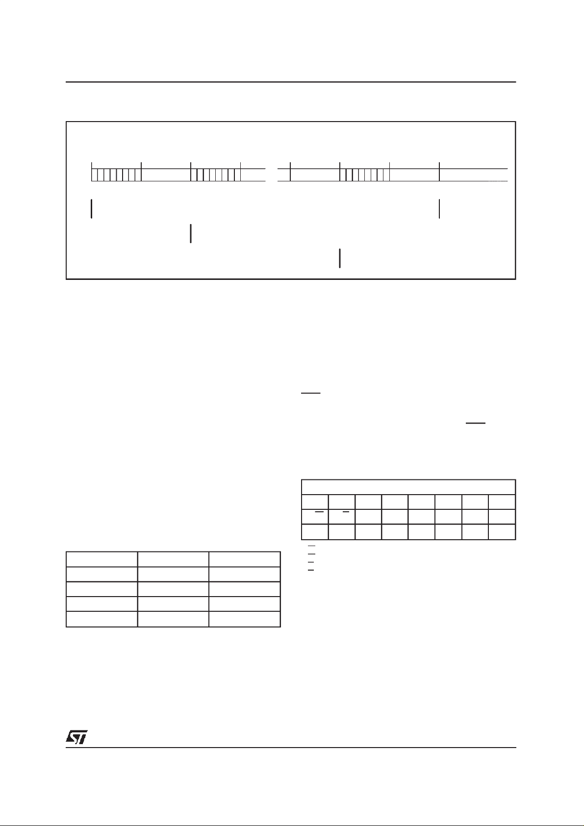
Figure 4. Pin Strap mode: TimeSlot Assignment
Receive /Transmit
Time Slot
CH0 CHn CHm
STLC5046
D7..................D0 D7...................D0
FS0
FSn
register.
DX represent the transmit PCM interface. It re-
mains in high impedance state except during the
assigned time slots during which the PCM data
byte is shifted out on the rising edge of MCLK.
The four channels can be shifted out in any possible timeslot as defined by the DXA0 to DXA3
registers. If one codec is set in Power Down by
software programmingthe correspondingtimeslot
is set in High Impedance. When linear coding
mode is selectedby CONF register programming
the output channel will need two consecutive
timeslots(see registerdescription).
DR represent the receive PCM interface. It remains inactive except during the assigned time
slots during wich the PCM data byte is shifted in
on the falling edge of MCLK. The four channels
are shifted in any possible timeslot as defined by
the DRA0 to DRA3 registers.
Pin StrapMode
When pinstrap mode is selected, dedicated
Frame Sync. FS3..0 are provided on dual function pins:
MCU Pin-strap Pin
FS FS0 12
IO4 FS1 17
IO5 FS2 18
IO6 FS3 48
The PCMSHregister cannot be accessed,therefore the beginning of the transmit and receive
frame is identified by the rising edge of the FSn
signal.
Each channel has its dedicated Frame Sync.signal FSn. Short or Long frame timing is automatically selected; depending on the FS signal applied to FS0 input. The assigned Time Slot
TS23/31/61/127D7...................D0
FSm
(Transmit and Receive) takes place in the 8
MCLK cycles following the falling edge of FSn in
case of Short Frame or the rising edge in case of
Long Frame. If one codec is set in Power Down
by proper pin strap configuration the corresponding timeslot is not loaded and the VFRO output is
kept at steady AGND level.
Finally by means of the LOOPB register is possible to implement a digital or analog loopback on
any of the selected channels.
TSX represent the Transmit Time Slot (open
drain output, 3.2mA). Normally it is floating in
high impedance state except when a time slot is
active on the DX output. In this case TSX output
pulls low to enable the backplane line driver.
Should be strapped to VSS when not used.
Table 1. Control byte structure.
First Byte (Address)
76543210
R/W D/S A5 A4 A3 A2 A1 A0
D7 D6 D5 D4 D3 D2 D1 D0
R/W = 0: Write Register
R/W = 1: Read Register
D/S = 0:Single byte
D/S = 1:Two bytes
A5..A0: Register Address
CONTROL INTERFACE
STLC5046 has two control modes, a microproc-
essor control mode and a pin strap controlmode.
The two modes are selected by M0 and M1 pins.
When M0 = low, M1 = high (MCU control mode)
the MCU port is activated;and the 41 registers of
the device can be programmed.When M0 = high,
M1 = low (Pin-strap mode) the microprocessor
control port is disabled and some of the digital
pins change their function allowing to perform a
very basic programmingof the device.
9/27
Page 10

STLC5046
In pin-strap mode the statusof the control pins is
entered at power-on reset and refreshed at any
Frame Sync. cycle.
In MCU mode the control information is written to
or read from STLC5046 via the serial four wires
control bus :
CCLK : ControlClock
CS : Chip Select input
CI : Serial Data input
CO : Serial Data output
All controlinstructions require 2 bytes,with theex-
ceptionof the single byte for commandsynchronization. The first byte specify the register address,
and thetypeof access(Reador Write).
The secondbyte containthe data to be loadedinto
the register (on CI wire) or carried out the register
content (on CO wire) depending on the R/W bit of
the first byte. CO wire is normally in High Impedance and goes to low impedance only during the
secondbytein case of Readoperation.Thisallows
to usea commonwireforboth CI/CO.
Serial data CI is shifted to the serial input register
on the rising edge of CCLK and CO is shiftedout
on the falling.
CS, normally High, is set Low during the transmission / reception of a byte, lasting 8CCLK
pulses .
Though, in general, two bytes of the same instruction take two CS separated cycles ,
STLC5046can handle the data transfer in a single 16 CCLK CS cycle, in both the directions.
One additional wire provided to the control interface is an open drain interrupt output (INT) that
goes low when a change of statusis detectedon
the I/O pins.
SLIC CONTROLINTERFACE
The device provides12 I/O pins plus4 CS signals.
Theinterfacecanworkin dynamicor staticmode:it
canbe selectedby meansof DIR register.
Dynamic Mode: the I/O pins are configured as
input or output by means of DIR register. The
CS signalsare used to selectthe differentSLIC
interface. In this case the I/O pin can be multiplexed. The data loaded from SLIC#n via I/O
pins configured as input can be read in the
DATAn register. The data written in a DATAn
registerwillbe loadedonthe I/O pinsconfigured
as outputwhentheCsnsignalwillbe active.
StaticMode: The CSsignal can be used as I/O
pins. They can be configured as input or output I/O by means of DATA1 register. The data
corresponding to the CS signal can be read or
written by means of DATA2 register. All data
related to th otherI/O pins can beread or written by meansof DATA0 register.
REGISTERSADDRESSES (only MCU mode)
Addr. Name Description
00h CONF Configuration Register
01h DIR-L I/O Direction (bit 7-0)
02h DIR-H I/O Direction (bit 11-8)
03h DATA0-L I/O Data ch#0/ Static Data;
(bit 7-0)
04h DATA0-H I/O Datach#0/ Static Data ;
(bit 11-8)
05h DATA1-L I/O Data ch#1 (bit 7-0) / CS
Direction
06h DATA1-H I/O Datach#1 (bit 11-8)
07h DATA2-L I/O Data ch#1 (bit 7-0) / CS
Data
08h DATA2-H I/O Datach#2 (bit 11-8)
09h DATA3-L I/O Data ch#3 (bit 7-0)
0Ah DATA3-H I/O Datach#3 (bit 11-8)
0Bh GTX0 Transmit Gain ch#0
0Ch GTX1 Transmit Gain ch#1
0Dh GTX2 Transmit Gain ch#2
0Eh GTX3 Transmit Gain ch#3
0Fh GRX0 Receive Gain ch#0
10h GRX1 Receive Gain ch#1
11h GRX2 Receive Gain ch#2
12h GRX3 Receive Gain ch#3
13h DXA0 Transmit Timeslot ch#0
14h DXA1 Transmit Timeslot ch#1
15h DXA2 Transmit Timeslot ch#2
16h DXA3 Transmit Timeslot ch#3
17h DRA0 Receive Timeslot ch#0
18h DRA1 Receive Timeslot ch#1
19h DRA2 Receive Timeslot ch#2
1Ah DRA3 Receive Timeslot ch#3
1Bh PCMSH PCM Shift Register
1Ch DMASK-L Interrupt Mask I/O Port (03h)
1Dh DMASK-H Interrupt Mask I/O Port (04h)
1Eh CMASK Interrupt Mask I/O Port (07h)
1Fh PCHK-A PersistencyCheck Time for
Input A
20h PCHK-B PersistencyCheckTimefor
Input B
21h INT Interrupt Register
22h ALARM Alarm Register
23h AMASK Interrupt Mask for Alarm
24h LOOPB Loopback Register
25h TXG Transmit preamp. Gain
26h RXG-1,0 Receivepreamp. Gain(ch1 ch0)
27h RXG-3,2 Receivepreamp. Gain(ch3 ch2)
31h SRID Siliconrevision identification
code
10/27
Page 11

STLC5046
REGISTERSDESCRIPTION
ConfigurationRegister(CONF)
Addr=00h;Reset Value=3Fh
Bit7 Bit6 Bit5 Bit4 Bit3 Bit2 Bit1 Bit0
RES LIN AMU STA PD3 PD2 PD1 PD0
RES=0Normal Operation
RES=1 Device Reset: I/0nand CSn are all inputs,
DX is H.I. (equivalent to Hw.reset).
LIN=0 A orµlaw PCM encoding
LIN=1 Linearencoding (16 bits), two’s comple-
ment.
AMU=0µ law selection
AMU=1 A law selection (even bits inverted)
STA=0 CS0 to CS3 scan the four SLICs con-
nected to the I/O control port, each CS has a
31.25µs repetitiontime.
STA=1; I/O are static, CS0 to CS3 are config-
ured as generic staticI/O
PD3..0=0Codec 3..0 is active
PD3..0=1 Codec 3..0 is in power Down. When
one codec is in Power Down the corresponding
VFRO output is forced to AGND. and the corresponding transmit time slot on DX is setin H.I.
Pin strap value:
RES 0 AMU 0 PD3 PD2 PD1 PD0
I/O Direction Register (DIR)
Addr=01h;Reset Value=00h
Addr=02h;Reset Value=X0h
Bit7 Bit6 Bit5 Bit4 Bit3 Bit2 Bit1 Bit0
IO7 IO6 IO5 IO4 IO3 IO2 IO1 IO0
IO11 IO10 IO9 IO8
IO
= 0; I/O pin 11..0 is an input, data on the
11..0
I/O input is written in DATAnregister bit 11..0.
IO
11
= 1; I/O pin 11..0 is an output, data con-
..0
tained in DATAn register bit11..0is transferredto
the I/O output.
Pin strap value:
00000000
00000000
I/O Data Register channel #0 (DATA0)
Addr=03h;Reset Value=00h
Addr=04h;Reset Value=X0h
If bit 4 of CONFregister (STA)=0
DynamicI/O mode:
Bit7 Bit6 Bit5 Bit4 Bit3 Bit2 Bit1 Bit0
D0
D06D05D04D03D02D01D0
7
D011D010D09D0
0
8
When CS0 is active D011..0 are transferredto the
corresponding I/O pins configured as outputs
(see DIR register). For the I/O pins configured as
11..0
inputs the corresponding D0
will be written by
the valuesapplied to those pins while CS0 is low.
If bit 4 of CONFregister (STA)=1
Static I/O mode:
Bit7 Bit6 Bit5 Bit4 Bit3 Bit2 Bit1 Bit0
DS
7 DS6 DS5 DS4 DS3 DS2 DS1 DS0
DS11DS10DS9DS
8
D11..0 are transferred to the corresponding I/O
pins configured as outputs(see DIR register). For
the I/O pins configured as inputs the correspond-
11..0
ing D
will be written by the values applied to
those pins.
Pin strap value:
00000000
0000
I/O Data Register channel #1 (DATA1)
Addr=05h;Reset Value=00h
Addr=06h;Reset Value=X0h
If bit 4 of CONFregister (STA)=0
DynamicI/O mode:
Bit7 Bit6 Bit5 Bit4 Bit3 Bit2 Bit1 Bit0
D1
D16D15D14D13D12D11D1
7
D111D110D19D1
0
8
When CS1 is active D11..0 are transferred to the
corresponding I/O pins configured as outputs
(see DIR register). For the I/O pins configured as
inputs the corresponding D
11..0 will be written by
the valuesapplied to those pins while CS1 is low.
If bit 4 of CONFregister (STA)=1
11/27
Page 12

STLC5046
Static I/O mode:
Bit7 Bit6 Bit5 Bit4 Bit3 Bit2 Bit1 Bit0
CIO
CIO2CIO1CIO
3
0
CIO0..3=0 The CS0..3 is a static input, DATA is
written in DATA2 register bits 0..3.
CIO0..3=1 The CS0..3 is a static output, DATA is
taken fromDATA2 registerbits 0..3.
Pin strap value:
00000000
0000
I/O Data Register channel #2 (DATA2)
Addr=07h;Reset Value=00h
Addr=08h;Reset Value=X0h
If bit 4 of CONF register(STA)=0
DynamicI/O mode:
Bit7 Bit6 Bit5 Bit4 Bit3 Bit2 Bit1 Bit0
D2
D26D25D24D23D22D21D2
7
D211D210D29D2
0
8
I/O Data Register channel #3 (DATA3)
Addr=09h;Reset Value=00h
Addr=0Ah;Reset Value=X0h
Used only if bit 4 of CONF register (STA)=0; Dynamic I/Omode:
Bit7 Bit6 Bit5 Bit4 Bit3 Bit2 Bit1 Bit0
D3
D36D35D34D33D32D31D3
7
D311D310 D39 D38
0
When CS3 is active D11..0 are transferred to the
corresponding I/O pins configured as outputs
(see DIR register). For the I/O pins configured as
inputs the corresponding D11..0 will be written by
the valuesapplied to those pins while CS3 is low.
If bit4 of CONF register(STA)=1
Static I/O mode:
can be used as general purpose R/W registers,
without any direct actionon the control of the device.
Pin strap value:
00000000
0000
TransmitGain channel #0 (GTX0)
Addr=0Bh;Reset Value=00h
When CS2 is active D2
11..0
are transferred to the
corresponding I/O pins configured as outputs
(see DIR register). For the I/O pins configured as
inputs the corresponding D11..0 will be written by
the values applied to those pins while CS2 is low.
If bit 4 of CONF register(STA)=1
Static I/O mode:
Bit7 Bit6 Bit5 Bit4 Bit3 Bit2 Bit1 Bit0
CD
CD2CD1CD
CD
3
3..0
are transferred to the corresponding CS
0
pin if configured as static output (see register
DATA1). For the CS pins configured as static inputs the corresponding CD
3..0 will be written by
the values applied to those pins.
Pin strap value:
00000000
0000
Bit7 Bit6 Bit5 Bit4 Bit3 Bit2 Bit1 Bit0
00h:Stop any trasmit signal, null level is transmitted in the correspondingtimeslot on DXoutput.
>00h:Digital gain is inserted in the TX path equal
to:
20log[0.25+0.75*(progr.value/256)]
Pin strap values:
GX0=1: 0dB gain (value = FFh):
11111111
GX0=0: -3.5dB gain (value = 8Fh):
10001111
TransmitGain channel #1 (GTX1)
Addr=0Ch; Reset Value=00h
Bit7 Bit6 Bit5 Bit4 Bit3 Bit2 Bit1 Bit0
00h:Stop any trasmit signal, null level is transmit-
12/27
Page 13

STLC5046
ted in the correspondingtimeslot on DX output.
>00h:Digitalgainisinsertedin theTXpathequalto:
20log[0.25+0.75*(progr.value/256)]
Pin strap values:
GX0=1: 0dB gain (value = FFh):
11111111
GX0=0: -3.5dB gain (value = 8Fh):
10001111
TransmitGain channel #2 (GTX2)
Addr=0Dh; Reset Value=00h
Bit7 Bit6 Bit5 Bit4 Bit3 Bit2 Bit1 Bit0
00h: Stop any trasmit signal, null levelis transmitted in the correspondingtimeslot on DX output.
>00h:Digitalgainisinsertedin theTXpathequalto:
20log[0.25+0.75*(progr.value/256)]
Pin strap values:
GX0=1: 0dB gain (value = FFh):
11111111
Receive Gain channel #0 (GRX0)
Addr=0Fh;Reset Value=00h
Bit7 Bit6 Bit5 Bit4 Bit3 Bit2 Bit1 Bit0
00h:Stop any received signal, AGND level is
forced on the VFRO0analog output.
>00h:Digitalgainisinsertedin theRXpathequalto:
20log[0.25+0.75*(progr.value/256)]
Pin strap values:
GR0=1: -0.8dB gain (value = E2h):
11100010
GR0=0: -2.36dB gain (value = AFh):
10101111
Overall gain includingalso RXG:
GR0 = 1:-0.8dB;GR0 = 0: -4.3dB
Receive Gain channel #1 (GRX1)
Addr=10h;Reset Value=00h
Bit7 Bit6 Bit5 Bit4 Bit3 Bit2 Bit1 Bit0
GX0=0: -3.5dB gain (value = 8Fh):
10001111
TransmitGain channel #3 (GTX3)
Addr=0Eh;Reset Value=00h
Bit7 Bit6 Bit5 Bit4 Bit3 Bit2 Bit1 Bit0
00h:Stop any trasmit signal, null level is transmitted in the correspondingtimeslot on DX output.
>00h:Digitalgainisinsertedin theTXpathequalto:
20log[0.25+0.75*(progr.value/256)]
Pin strap values:
GX0=1: 0dB gan (value= FFh):
11111111
GX0=0: -3.5dB gain (value = 8Fh):
10001111
00h:Stop any received signal, AGND level is
forced on the VFRO1analog output.
>00h:Digitalgainisinsertedin theRXpathequalto:
20log[0.25+0.75*(progr.value/256)]
Pin strap values:
GR1=1: -0.8dB gain (value = E2h):
11100010
GR1=0: -2.36dB gain (value = AFh):
10101111
Overall gain includingalso RXG:
GR1= 1:-0.8dB;GR1 = 0: -4.3dB
Receive Gain channel #2 (GRX2)
Addr=11h;Reset Value=00h
Bit7 Bit6 Bit5 Bit4 Bit3 Bit2 Bit1 Bit0
00h:Stop any received signal, AGND level is
forced on the VFRO2analog output.
>00h:Digitalgainisinsertedin theRXpathequalto:
13/27
Page 14

STLC5046
20log[0.25+0.75*(progr.value/256)]
Pin strap values:
GR2=1: -0.8dB gain (value= E2h):
11100010
GR2=0: -2.36dB gain (value= AFh):
10101111
Overall gain includingalso RXG:
GR2 = 1:-0.8dB;GR2 = 0: -4.3dB
Receive Gain channel #3 (GRX3)
Addr=12h;Reset Value=00h
Bit7 Bit6 Bit5 Bit4 Bit3 Bit2 Bit1 Bit0
00h:Stop any received signal, AGND level is
forced on the VFRO3 analog output.
>00h:Digitalgainisinsertedin theTXpathequalto:
20log[0.25+0.75*(progr.value/256)]
Pin strap values:
GR3=1: -0.8dB gain (value= E2h):
11100010
GX3=0: -4.3dB gain (value = AFh):
10101111
Overall gain includingalso RXG:
GR3 = 1:-0.8dB;GR3 = 0: -4.3dB
Example: if T06..T00=00:
TS0 TS1
1514131211109876543210
Pin strap value (value 80h):
10000000
Referredto FS0.
TransmitTime Slotchannel#1 (DXA1)
Addr=14h;Reset Value=00h
Bit7 Bit6 Bit5 Bit4 Bit3 Bit2 Bit1 Bit0
EN1 T16 T15 T14 T13 T12 T11 T10
EN1=0: Selectedtransmittime slot on DX output
is in H.I.
EN1=1: Selectedtransmittime slot on DX output
is activecarryingout the PCM encoded
signalof VFXI1.
T16..0:Define time slot number (0 to 127) on
which PCM encoded signal of VFXI1 is carried
out.
If linear mode is selected (LIN=1 of CONF register) the 16 bits will be carried out as follows:the 8
most significative bits in the programmed time
slot, the 8 least significative bits in the following
timeslot.
Example: if T16..T10=00:
TS0 TS1
1514131211109876543210
Pin strap value (value=80h)
TransmitTime Slotchannel #0 (DXA0)
Addr=13h;Reset Value=00h
Bit7 Bit6 Bit5 Bit4 Bit3 Bit2 Bit1 Bit0
EN0 T06 T05 T04 T03 T02 T01 T00
EN0=0: Selectedtransmit time slot on DX output
is in H.I.
EN0=1: Selectedtransmit time slot on DX output
is activecarryingout the PCM encoded
signalof VFXI0.
T06..0: Define time slot number (0 to 127) on
which PCM encoded signal of VFXI0 is
carriedout.
If linear mode is selected (LIN=1 of CONF register) the 16 bits will be carried out as follows: the 8
most significative bits in the programmed time
slot, the 8 least significative bits in the following
timeslot.
14/27
10000000
Referredto FS1.
TransmitTime Slotchannel #2 (DXA2)
Addr=15h;Reset Value=00h
Bit7 Bit6 Bit5 Bit4 Bit3 Bit2 Bit1 Bit0
EN2 T26 T25 T24 T23 T22 T21 T20
EN2=0: Selectedtransmittime slot on DX output
is in H.I.
EN2=1: Selectedtransmittime slot on DX output
is activecarryingout the PCM encoded
signalof VFXI2.
T26..0:Define time slot number (0 to 127) on
which PCM encoded signal of VFXI2 is carried
out.
If linear mode is selected (LIN=1 of CONF regis-
Page 15

STLC5046
ter) the 16 bits will be carried out as follows: the 8
most significative bits in the programmed time
slot, the 8 least significative bits in the following
timeslot.
Example: if T26..T20=00:
TS0 TS1
15 14 13 12 11 10 9 8 7 6 5 4 3 2 1 0
Pin strap value (value=80h)
10000000
Referredto FS2.
TransmitTime Slotchannel #3 (DXA3)
Addr=16h;Reset Value=00h
Bit7 Bit6 Bit5 Bit4 Bit3 Bit2 Bit1 Bit0
EN3 T36 T35 T34 T33 T32 T31 T30
EN3=0: Selectedtransmit time slot on DX output
is in H.I.
EN3=1: Selectedtransmit time slot on DX output
is activecarryingout the PCM encoded
signalof VFXI3.
T36..0:Define time slot number (0 to 127) on
which PCM encoded signal of VFXI3 is carried
out.
If linear mode is selected (LIN=1 of CONF register) the 16 bits will be carried out as follows: the 8
most significative bits in the programmed time
slot, the 8 least significative bits in the following
timeslot.
Example: if T36..T30=00:
TS0 TS1
15 14 13 12 11 10 9 8 7 6 5 4 3 2 1 0
Pin strap value (value=80h)
10000000
on carrying the PCM signal to be decoded and
tranferred to VFRO0 output.If linear mode is selected (LIN=1 of CONF register) the 16 bits will
be used as linear code as follows: the 8most significative bits in the programmed time slot, the 8
least significative bits in the followingtimeslot.
Example: if R06..R00=00:
TS0 TS1
1514131211109876543210
Pin strap value (value 80h):
10000000
Referredto FS0.
Receive Time Slot channel #1 (DRA1)
Addr=18h;Reset Value=00h
Bit7 Bit6 Bit5 Bit4 Bit3 Bit2 Bit1 Bit0
EN0 R16 R15 R14 R13 R12 R11 R10
EN1=0: Disablereceptionof selectedtime slot.
EN1=1: Selectedreceivetime sloton DRinput is
PCM decoded and tranferred to VFRO1
output.
R16..0:Definereceive time slot number (0 to 127)
on carrying the PCM signal to be decoded and
tranferred to VFRO1 output.If linear mode is selected (LIN=1 of CONF register) the 16 bits will
be used as linear code as follows: the 8most significative bits in the programmed time slot, the 8
least significative bits in the followingtimeslot.
Example: if R16..R10=00:
TS0 TS1
1514131211109876543210
Pin strap value (value=80h)
10000000
Referredto FS3.
Receive Time Slot channel#0 (DRA0)
Addr=17h;Reset Value=00h
Bit7 Bit6 Bit5 Bit4 Bit3 Bit2 Bit1 Bit0
EN0 R06 R05 R04 R03 R02 R01 R00
EN0=0: Disablereception of selected time slot.
EN0=1: Selectedreceive timeslot on DRinput
isPCM decodedandtranferr edto VFRO0
output.
R06..0:Definereceive time slot number (0 to 127)
Referredto FS1.
Receive Time Slot channel #2 (DRA2)
Addr=19h;Reset Value=00h
Bit7 Bit6 Bit5 Bit4 Bit3 Bit2 Bit1 Bit0
EN2 R26 R25 R24 R23 R22 R21 R20
EN2=0: Disablereceptionof selectedtime slot.
EN2=1: Selectedreceivetime sloton DRinput is
PCM decoded and tranferred to VFRO1
output.
R26..0:Definereceive time slot number (0 to 127)
15/27
Page 16

STLC5046
on carrying the PCM signal to be decoded and
tranferred to VFRO2 output.If linear mode is selected (LIN=1 of CONF register) the 16 bits will
be used as linear code as follows: the 8most significative bits in the programmed time slot, the 8
least significativebitsin the followingtimeslot.
Example: if R26..R20=00:
TS0 TS1
15 14 13 12 11 10 9 8 7 6 5 4 3 2 1 0
Pin strap value (value=80h)
10000000
Referredto FS2.
Receive Time Slot channel#3 (DRA3)
Addr=1Ah;Reset Value=00h
Bit7 Bit6 Bit5 Bit4 Bit3 Bit2 Bit1 Bit0
EN3 R36 R35 R34 R33 R32 R31 R30
EN3=0: Disablereception of selected time slot.
EN3=1: Selectedreceive timeslot on DRinput is
PCM decoded and tranferred to VFRO1
output.
R36..0:Definereceive time slot number (0 to 127)
on carrying the PCM signal to be decoded and
tranferred to VFRO2 output.If linear mode is selected (LIN=1 of CONF register) the 16 bits will
be used as linear code as follows: the 8most significative bits in the programmed time slot, the 8
least significativebitsin the followingtimeslot.
Example: if R36..R30=00:
TS0 TS1
15 14 13 12 11 10 9 8 7 6 5 4 3 2 1 0
Pin strap value (value=80h)
10000000
Referredto FS3.
PCM Shift Register (PCMSH)
Addr=1Bh;Reset Value=00h
Bit7 Bit6 Bit5 Bit4 Bit3 Bit2 Bit1 Bit0
XS2 XS1 XS0 RS2 RS1 RS0
XS2..0:Effective start of the TX frame is the programmed values of clock pulses (0 to 7) after the
FS risingedge.
RS2..0:Effectivestart of the RX frame is the programmed values of clock pulses (0 to 7) after the
FS rising edge.
Pin strap value (value=00h):
00000000
Interrupt Mask Registerfor I/O port (DMASK)
Addr=1Ch; Reset Value=FFh
Addr=1Dh; Reset Value=XFh
Bit7 Bit6 Bit5 Bit4 Bit3 Bit2 Bit1 Bit0
MD7 MD6 MD5 MD4 MD3 MD2 MD1 MD0
MD11 MD10 MD9 MD8
MD11..0=1: The corresponding I/O doesn’t generate interrupt.
MD11..0=0: The corresponding I/O (programmed
as Input) generate interrupt if a change of status
is detected.
Input lines with persistency check generate interrupt if thechanged status remains stable longer
than the time programmed in the persistency
check registers PCHKA/B. Lines without persistance check generate an immediate interrupt request.
Mask register has no effect on those pins configured as outputs, those pins will not generate interrupt.
Pin strap value.
11111111
1111
Interrupt Mask Registerfor CD port (CMASK)
Addr=1Eh;Reset Value=XFh
Bit7 Bit6 Bit5 Bit4 Bit3 Bit2 Bit1 Bit0
MC3 MC2 MC1 MC0
In MCU mode, dynamic I/O configuration, MCn
bits are the disable/enable interrupt related to the
channeln :
MC3..0= 0 Any I/O line of the related channel is
enabled to generate interrupt depending on
DMASKsetting.
MC3..0=1 Any I/O line of the related chanel is
disabled to generate interrupt indipendently of
DMASKsetting.
In MCU mode, static I/O configuration, MCn bits
are the interrupt mask bits related to CSn that
are configuredas I/O lines.
MC3..0=1: The corresponding I/O doesn’t generate interrupt.
MC3..0=0:The corresponding I/O generateinterrupt if a change of statusis detected.
16/27
Page 17

STLC5046
Input lines with persistency check generate interrupt if the changed status remains stable longer
than the time programmend in the persistency
check registers PCHKA/B
Lines without persistency check generate an immediate interrupt request.
Mask register has no effect on those pins configured as outputs, those pins will not generate interrupt.
Pin strap value (value=00h):
11111111
PersistencyCheck Register (PCHK-A/B)
Two input signals per channel , labeled A and B,
are submittedto persistencycheck.
In dynamic mode (STA=0), A and B inputs of the
four channels, are sampled on the multiplexed
lines IO0 (pin13) and IO1 (pin14).
In static mode (STA=1) the persistency check is
performed on four pairs of lines, assigned to
each channelaccordingto thetable:
CHAN# Input A Input B
0 IO0 (pin 13) IO1 (pin14)
1 IO4 (pin 17) IO5 (pin18)
2 IO6 (pin 48) IO7 (pin47)
3 IO10 (pin 44) IO11 (pin43)
00000000
00000000
Interrupt Register(INT)
Addr=21h;Reset Value=00h
Bit7 Bit6 Bit5 Bit4 Bit3 Bit2 Bit1 Bit0
ICKF ID3 ID2 ID1 ID0
ICKF = 1: If interrupt is generatedby a changeof
bit 0 in registerALARM.
In dynamic I/O configuration the ID3..0 bits
latch the interrupt request from the relatedchannel.
Any single bit IDn is cleared after reading related
I/O register or by setting MCn bit High (i.e. when
channeln is disabled to generate interrupt).
In static I/O configuration ID0 and ID2 bits latch
the interrupt requestfrom I/O11..0 and CS3..0respectively:
ID0 : is set High when the interrupt is requested
fromany the I/O11..0 lines.
ID2: is set High when the interrupt is requested
fromany of the CS3..0 (configuredas I/O).
ID0 and ID2 are cleared after reading related I/O
register.
ID1 and ID3 are don’t care.
Pin strap value (value=00b):
00000
Addr=1Fh; ResetValue=00h
Addr=20h; ResetValue=00h
Bit7 Bit6 Bit5 Bit4 Bit3 Bit2 Bit1 Bit0
TA7 TA6 TA5 TA4 TA3 TA2 TA1 TA0
TB7 TB6 TB5 TB4 TB3 TB2 TB1 TB0
TA7..0 and TB7..0, content of PCHKA and
PCHKB registers, define the minimum duration
of input A and B to generate interrupt ; spurious
transitions shorter than the programmed value
are ignored.
The time width can be calculated according to
the formula:
Time-WidthA = (TA7..0) x 64µs
Time-WidthB = (TB7..0) x 64µs
If PCHKA/B is programmed to 00h the persist-
ency check is not performed and any detected
transitionwill generate interrupt.
All the inputs, with or without persistency check,
are sampled with a repetition rate of 32µs
Pin strap value:
Alarm Register (ALARM)
Addr=22h;Reset Value=00h
Bit7 Bit6 Bit5 Bit4 Bit3 Bit2 Bit1 Bit0
POR CKF
CKF=1: If number of PCM clock pulses in one
frameperiod does not match expectedvalue.
POR=1: If a Power On Reset is detected during
operation.
The register ALARM is cleared after reading operation only if signals are inactive.
Pin strap value (value=00h):
00
Interrupt Mask Registerfor Alarm (AMASK)
Addr=23h;Reset Value=11b
Bit7 Bit6 Bit5 Bit4 Bit3 Bit2 Bit1 Bit0
MCF
17/27
Page 18

STLC5046
MCF=1: The corresponding alarm bit (CKF)
doesn’t generate interrupt.
MCF=0: The corresponding alarm bit (CKF) generates interrupt.
Pin strap value (value=00h):
1
Loopback Register (LOOPB)
Addr=24h;Reset Value=00h
Bit7 Bit6 Bit5 Bit4 Bit3 Bit2 Bit1 Bit0
DL3 DL2 DL1 DL0 AL3 AL2 AL1 AL0
DL3..0=0:Normal Operation
DL3..0=1:Codec #3..0 is set in DigitalLoopback
mode, this means that the receive PCM
signalapplied to the programmed
Receive Time Slot is transferred to the
programmedTransmitTime Slot.
AL3..0=0:NormalOperation
AL3..0=1:Codec #3..0is set in AnalogLoopback
mode, this means that the VFRO signal
is tranferredto the VFXIinput internally
into the Codec.
When loopbacks are enabled the signal appears
also at the corresponding VFRO output. It is possible to have no signal on the VFRO output programmingthe GR registerto 00h in case of digital
loopback.
Pin strap value (value=00h):
00000000
TransmitPreamplifierGain Register (TXG)
Addr=25h;Reset Value=X0h
Bit7 Bit6 Bit5 Bit4 Bit3 Bit2 Bit1 Bit0
XG3 XG2 XG1 XG0
XG3..0=0:Transmi tpreamplifiergainch. 3..0= 0dB
XG3..0=1:Transmi tpreamplif i ergainch.3..0=3.52dB
Overall transmit gain depends on combination of
TXG and GTXn registers. For XGn=0 and
GTXn=FF 0dBm0 at DX output correspond to 15dBm|
(137mVrms)at VFXI input.
600Ω
Pin strap value (value=00h):
0000
Receive Amplifier Gain Registers (RXG-10/32)
Addr: 26h; Reset Value=00h
Addr: 27h; Reset Value=00h
Bit7 Bit6 Bit5 Bit4 Bit3 Bit2 Bit1 Bit0
R12 R11 R10 R02 R01 R00
R32 R31 R30 R22 R21 R20
Rn2 Rn1 Rn0 Receive Amplifier Gain
Ch#n (dB)
000 Mute
0 0 1 -13.98
0 1 0 -7.96
0 1 1 -4.44
1 0 0 -1.94
101 0
110 0
111 0
Overall receive gain depends on the receive amplifier gain (Rn2..0 settingin RXG reg.)and
digital gain (GRXn reg. setting).
As a reference : when Rn2..0 is set for 0dB gain
and GRXn=FFh (max. gain) 0dBm0 at DR input
correspond to a level at VFRO output equal to
547mVrms(e.g. -3dBm 600ohm)
Pin strap value :
Rn2 Rn1 Rn0
GRn = 1 1 1 1
GRn = 0 1 0 0
Overall gain includingalso GRXn;
GRn = 1: -0.8dB; GRn = 0:-4.3dB.
Silicon Revision Identification Code (SR=D)
Addr: 31h;Read Only.
XXXX0000
18/27
Page 19

STLC5046
Figure 5. Typical Application Circuit with STLC3080 withoutMeteringPulse injection and I/O
pins in dynamic mode.
(5V)
CC
(3.3V) V
DD
V
BGND REL0
AGND
CC
V
DD
V
REL1
133729109
ZAC1
TIP
P2
R
RT
VREL
CAC
RDC
ILTF
RDC
RELR
25
14
12
GRX=+6dB
21
20
19
RS
ZAC
RS
26
GTX=-12dB
18
ZB
CAC
22
RX
P1
R
TIP
24
39
41
TX
MODE
LCP
1511
BAT
V
PCD
40
STLC3080
43
17
DET
GDK/AL
RING
P2
R
RR
P1RS1RS2
R
RING
RT1
28
38
4
5
44
3
D2
D0
D1
shorted
VRING
BAT
V
QEXT
VREG
BASE
RT2
363516
27
6
7
1
R0
R1
CSIN
CSOUT
VBAT
2
RES
CVB
8
RTH
BAT
V
CSRV
34
30
33
32
31
23 42 11
CREV
IREF
RLIM
TTXIN CKRING CRT
CREV CSRV
REF
CRT
RTH RLIM
AGND and BGND must be
together on the LINE CARD
D99TL430
(3.3V)
CC
V
CC
RAC
ZA
IO7
IO8
IO9
IO10
IO11
CC
6160595857
0.1µF
CC
V
CRX
ZB
CH
VFRO0
33
CTX 100nF
IO1
IO2
IO3
VFXI0
35192021222324
IO4
IO5
IO6
TO OTHERSLICs
CS1
CS2
CS0
28
62
295353393842434846
CS3
VFRO1
VFXI1
SLICs
TO OTHER
VFRO2
VFXI2
VFRO3
VFXI3
STLC5046 IO0
EE
V
8941
GND V
V
SS
DD
V
V
DD
SUB
0.1µF
DX
101114
DR
13
FS
MCLK
PCM
INTERFACE
TSX
12
27
54
3
475
6
M1
M0
INT
CC
V
CS
CO
CCLK
SERIAL
CONTROL
CI
PORTS
CAP
40
CAP
0.1µF
19/27
Page 20

STLC5046
ELECTRICALCHARACTERISTICS
(Typicalvalue 25°C and nomin alsupply voltage.Minimum and maximum value are guaranteedover the temperature0 to 70°Crangeby productiontestingand supplyvoltagerange shownin theOperating Ranges.Performancesover-40to+85°Careguaranteedby productcharacterisationunlessotherwi sespecif ied .)
DIGITALINTERFACE
Symbol Parameter Test Condition Min. Typ. Max. Unit
Vil Input Voltage Low DI pins 0 0.2V
Vih Input Voltage High DIpins(1) 0.8V
DD
Iil Input Current Low DI pins -10 10
Iih Input Current High DI pins -10 10 µA
Ci Input Capacitance (all dig. inp.) 5 pF
Vol Output VoltageLowDX, TSX pins Iol= 3.2mA(otherpinsIol= 1mA) 0 0.4 V
Voh Output VoltageHigh DX pinn Ioh= -3.2mA(otherpinsIol= 1mA) 0.85V
DD
ANALOG INTERFACE
5.5 V
VDD V
DD
V
A
µ
RIX Transmit Input Amplifier Input
1000 MΩ
Impedance (VFXI)
ROR Receive Output Impedance
1 Ω
(-1.0V< VFRO<1.0V,IVFRO=1mA
POWERDISSIPATION
Idd (pd) Power down Current 9 11 mA
Idd Active Current 48 60 mA
MASTER CLOCKTIMING
f
MCLK
t
WMH
t
WML
t
t
RM
FM
Frequency of MCLK frequency is automatically
detected
Period of MCLK high Measured from VIHto V
Period of MCLK low Measured from VILto V
Rise Time of MCLK Measured from VILto V
Fall Time of MCLK Measured from VIHto V
IH
IL
IH
IL
1.536
1.544
2.048
4.096
8.192
40 ns
40 ns
15 ns
15 ns
PCM INTERFACE TIMING
t
HMF
t
SFM
t
DMD
t
DMZ
t
SDM
t
HMD
t
DZC
t
XDP
(1) All the digital input are five-volt tollerant
- maximum DC voltage 5.5V
- maximum peakvoltage 6.5V
(2) Itisdefined as the time at which the output achivies the off state.
Hold Time MCLKlow to FS low 10 ns
SetupTime, FS hightoMCLK low 10 ns
Delay Time, MCLK high to data
valid
(2)
Delay Time, MCLK low to DX
disabled
Pull up resistor = 1kΩ
C
= 30pF
load
540ns
Setup Time,DRvalidtoMCLK low 15 ns
Hold Time, MCLK low to D
R
5ns
invalid
(2)
DelayTime,MCLKlowtoTSXhigh Pull up resistor = 1kΩ
DelayTime,MCLKhightoTSXlow 10 ns
C
= 30pF
load
10 ns
40 ns
MHz
MHz
MHz
MHz
MHz
20/27
Page 21

Figure 6a. Pin-strap mode Short Frame Sync.Timing.
STLC5046
t
RM
MCLK
t
t
HMF
SFM
12345671617
t
WFH
FS
t
DMD
DX
DR
TSX
Note:T
t
XDP
has to be shorter than or equal to 3 MCLK period to select Short Frame.
WFH
1234567 16
t
SDMtHMD
1234567 16
Figure 6b. Pin Strap mode LongFrame Sync. Timing.
t
FM
t
WMH
t
WML
D98TL386C
t
DMZ
t
DZC
MCLK
FS
DX
DR
TSX
Note:T
t
HMF
12345671617
t
t
SFM
t
DMD
t
XDP
has to be longer than 3 MCLK period to select Long Frame.
WFH
1234567 16
1234567 16
WFH
t
RM
t
SDMtHMD
t
FM
t
WMH
t
WML
D98TL387C
t
DMZ
t
DZC
21/27
Page 22

STLC5046
Figure 6c. MCU Mode Frame Sync. Timing.
MCLK
FS
DX
DR
TSX
t
HMF
12345671617
t
SFM
t
t
DMD
XDP
1234567 16
1234567 16
t
RM
t
SDMtHMD
t
FM
t
WMH
t
WML
D98TL388C
t
DMZ
ELECTRICALCHARACTERISTICS (continued)
SERIALCONTROL PORTTIMING
Symbol Parameter TestCondition Min. Typ. Max. Unit
f
t
t
t
t
t
t
t
t
t
DDZ
t
t
CCLK
WCH
WCL
t
RC
t
FC
HCS
SSC
SDC
HCD
DCD
DSD
HSC
SCS
Frequency of CCLK 4.096 MHz
Period of CCLK high Measured fromVIHto V
Period of CCLK low Measured from VILto V
Rise Time of CCLK Measured from VILto V
Fall Time of CCLK Measured from VIHto V
IH
IL
IH
IL
100 ns
100 ns
HoldTime, CCLK highto CS– low 5 ns
SetupTime,CS–low toCCLKhigh 10 ns
Setup Time,CIvalid to CCLKhigh 20 10 ns
HoldTime,CCLKhigh to CI
10 ns
invalid
Delay Time, CCLK low to CO
data valid
Delay Time, CS–low to CO data
valid
(1)
DelayTime CS–high or 8th
CCLKlowtoCOhighimpedance
Pull up resistor = 1k
C
= 30pF
load
Ω
whichever comes first
Hold Time, 8th CCLK high to
10 ns
CS– high
SetupTime,CS–hightoCCLKhigh 10 ns
20 ns
20 ns
30 ns
20 ns
50 ns
t
DZC
(1) Itisdefined as the time at which the output achivies the off state.
22/27
Page 23

Figure 7. Serial control port timing.
STLC5046
CCLK
t
HCS
CS-
CO
CI
t
RC
123
t
SSC
76543210
45678 23456781
BYTE 1 BYTE 2
t
t
FC
SDC
t
HCS
t
HCD
t
SCS
t
WCH
t
HCS
t
SCS
t
e
t
DSD
65432107
t
DCD
t
WCL
D99TL454
t
HSC
t
DDZ
ELECTRICALCHARACTERISTICS (continued)
SLIC CONTROLINTERFACETIMING
Symbol Parameter Test Condition Min. Typ. Max. Unit
TCS Chip Select repetition rate 31.25 µs
tcsw Chip select pulse width 3.90 µs
t
DIV
t
t
DOA
t
DON
DII
Time CS low to data input valid 1.65 µs
Time data inputinvalid to CS high 1.65 µs
Time data outputavailable to CS low 1.8 µs
Time CS high to data output not available 1.8 µs
Figure 8. SLIC Control port timing.
t
t
DIV
OUT
CH0
IN
CH0
DII
t
DON
OUT
CH1
IN
CH1
CS1
CS2
CS3
CS4
IO
(OUT)
IO
(IN)
t
DOA
31.25µs (32KHz)
OUT
CH2
IN
CH2
OUT
CH3
IN
CH3
OUT
CH0
IN
CH0
OUT
CH1
IN
CH1
D99TL460
23/27
Page 24

STLC5046
TRANSMISSIONCHARACTERISTICS
TRANSMISSIONTRANSFER CHARACTERISTICS
Symbol Parameter Test Condition Min. Typ. Max. Unit
Absolute levels (see Table 19)
The nominal 0dBm0 levels are:
TXG = 0dB, GTXn = 0dB (FF) 137 mVrms
GXA Transmitgain Absolute accuracy -0.15 0.15 dB
GXAG Transmit gain variation with
GFX Gain variation with frequency
GAXT Gain variation with temperature -0.10 0.10 dB
GAXE Gain variation with Supplies
GTX Gain Tracking with Tone
QDX Quantization Distortion with
NCT Transmit Noise C Message
NPT Transmit Noise Psophometric
DDX
DAX
DPXM Single Frequency Distortion
DPXA Single Frequency Distortion
programmed gain (within 3dB
from max. dig. level)
(relative to gain at 1004Hz);
0dBm0 input signal
50Hz
60Hz
200Hz
300-3000Hz
3400Hz
4000Hz
4600Hz and above
±5% 0dBm0 InputSignal
(1004Hz µ Law, 820Hz ALaw)
Tone (1004HzµLaw, 820Hz
ALaw)
Weighted (µ Law)
Weighted (A Law)
(1)
Differential Envelope Delay (1
to 2.56KHz Input Sinewave @
0dBm0)
(1)
Absolute Delay @ 1KHz
500 to 2800Hz
(Mu Law 0dBm0 Sinewave @
1004Hz)
(ALaw0dBm0Sinewave@ 820Hz)
GSX = 3 to -40dBm0
GSX = -40 to -50dBm0
GSX = -50 to -55dBm0
VFXI = +3dbm0
VFXI = 0 to -30dBm0
VFXI = -40dBm0
VFXI = -45dBm0
500Hz
604Hz
1000Hz
1792Hz
2604Hz
2792Hz
RECEIVETRANSFERCHARACTERISTICS
-0.2 +0.2 dB
-20
-20
-1.8
-0.15
-0.7
-0.05 0.05 dB
-0.2
-0.4
-1.2
33
36
30
25
0
0.15
0
-14.0
-32.0
0.2
0.4
1.2
12 dBrnCo
-68 dBm0p
170
110
25
0
70
95
420 µs
-46 dB
-46 dB
dB
dB
dB
µs
Absolute levels
The nominal 0dBm) levels are
VFRO:
RGX = 0dB, GRXn = 0db (FF)
GRA Transmit gainAbsoluteaccuracy
(within 3dB frommax.dig. level)
(1) Typical value not tested in production.
24/27
547 mVrms
-0.15 0.15 dB
Page 25

STLC5046
TRANSMISSIONCHARACTERISTICS
RECEIVETRANSFERCHARACTERISTICS (continued)
Symbol Parameter Test Condition Min. Typ. Max. Unit
GRAG Receive Gain Variation with
programmed gain
GFR Gain variation with frequency
(relative to gain at 1004Hz);
0dBm0 input signal.
Below 200Hz
200Hz
300-3000Hz
3400Hz
4000Hz
GART Gain variation with temperature -0.1 +0.1 dB
GARE Gain variation with supplies 0dBm0 Input Signal
GTR Gain Tracking with Tone
(1004Hz Mu Law, 820Hz A
Law)
QDR Quantization Distortion with
Tone (1004Hz Mu Law, 820Hz
A law)
V
CC=VDD
DR = 3to -40dBm0
DR = -40to -50dBm0
DR = -50to -55dBm0
DR = 3dBm0
DR = 0to -30dBm0
DR = -40dBm0
= 3.3V ±5%
DR = -50to -55dBm0
GSPR Out of band spourious Noise
0dBm0 180 to 3400Hz
Sinewave at DR
NCR Receive Noise C Message
Weighted (µ Law)
NPR Receive Noise Psophometric
Weighted (A Law)
(1)
DDR
Differential Envelope Delay
(1 to 2.56kHz Input Sinewave
@ 0dBm0)
500Hz
604Hz
1000Hz
1792Hz
2604Hz
2792Hz
(1)
DAR
Absolute Delay @ 1kHz
500 to 2800Hz
DPR1 Single Frequency Distortion
(0dBm0 Sinewave @ 1004Hz)
PSRR Power Supply Rejection Ratio
1kHz, 50mVrms
CTX-R Transmit to Receive Crosstalk
(input signal 200Hz to 3450Hz
at 0dBm0)
CTR-X Receive to Transmit Crosstalk
(input signal 200Hz to 3450Hz
at 0dBm0)
CT-ICH Inter Channel Crosstalk, TX
and TX direction.
Input 200 to 3450Hzat 0dBm0
at VFXIof one channel;all
other VFXI inputs and all DR
inputs receive idle signal.
Output is measured at DX of
the 3 idle channels.
-0.2 +0.2 dB
0.15
-0.25
-0.15
-0.7
0.15
0.15
0
-14
-0.05 0.05 dB
-0.2
-0.4
-1.2
0.2
0.4
1.2
33
36
30
25
32 dB
8 11 dBrnCo
-82 -79 dBm0p
25
0
0
0
90
115
440 µs
-46 dB
30 dB
-76 dB
-76 dB
-78 dB
dB
dB
dB
µs
(1) Typical value not tested in production.
Input 200 to 3450Hzat 0dBm0
at DR of one channel; all other
DR inputs and all VFXI inputs
receive idle signal.
Output is measured at VFRO of
the 3 idle channels.
25/27
Page 26

STLC5046
DIM.
mm inch
MIN. TYP. MAX. MIN. TYP. MAX.
A 1.60 0.063
A1 0.05 0.15 0.002 0.006
A2 1.35 1.40 1.45 0.053 0.055 0.057
B 0.18 0.23 0.28 0.007 0.009 0.011
C 0.12 0.16 0.20 0.0047 0.0063 0.0079
D 12.00 0.472
D1 10.00
0.394
D3 7.50 0.295
e 0.50 0.0197
E 12.00 0.472
E1 10.00
0.394
E3 7.50 0.295
L 0.40 0.60 0.75 0.0157 0.0236 0.0295
L1 1.00 0.0393
K 0°(min.), 7°(max.)
OUTLINE AND
MECHANICAL DATA
TQFP64
D
D1
A1
TQFP64
16
3348
32
17
E3D3E1
E
L1
L
K
0.10mm
Seating Plane
49
B
64
1
e
A
A2
B
C
26/27
Page 27

STLC5046
Information furnished is believedto be accurate and reliable. However, STMicroelectronics assumes no responsibility for the consequences
of use of such information nor for any infringement of patents or other rights of third parties which may result from its use. No license is
granted by implication or otherwise under any patent or patent rights of STMicroelectronics. Specification mentioned in this publication are
subject to change without notice. This publication supersedes and replaces all information previously supplied. STMicroelectronics products
are not authorized for use as critical components in life support devices or systems without express written approval of STMicroelectronics.
The ST logois a registered trademark of STMicroelectronics
2000 STMicroelectronics – Printedin Italy – All Rights Reserved
STMicroelectronics GROUP OF COMPANIES
Australia - Brazil - China- Finland - France - Germany - Hong Kong - India - Italy- Japan - Malaysia - Malta - Morocco -
Singapore - Spain - Sweden - Switzerland - United Kingdom - U.S.A.
http://www.st.com
27/27
 Loading...