

Page 1

®
FOR SHORT LOOP APPLICATIONS
MONOCHIP SLIC SUITABLE FOR SHORT
LOOP APPL I CATIONS
IMPLEMENTES ALL KEY FEATURES OF
THE BORSHT FUNCTION
INTEGRATED RINGIN G
SOFT BATTERY REVERSAL WITH PRO-
GRAMMABLE TRANSITION TIME
ON HOOK TRANSMISSION
LOW POWER DISSIPATION IN ALL OPER-
ATING MODES
AUTOMATIC DUAL BATTERY OPERATION
INTEGRATED RING TRIP DETECTION
METERING PULSE INJECTION
LOOP START, GROUND START FEATURES
SURFACE MOUNT PACKAGE
-40 TO +85°C OPERATING RANGE
DESCRIPTION
The STLC30R80 is a SLIC device suitable for
short loop applications. The SLIC provides the
STLC30R80
INTEGRATED RINGING SLIC
TQFP44 (10 x 10)
ORDERING NUMBER:
generation of the ringing signal and the standard
battery feeding with full programmability of the DC
characteristic.
In particular two external resistors allow to set the
limiting current value (up to 50mA) and the value
of the resistive feeding when not in constant current region.
STLC30R80
BLOCK DIAGRAM
DET
GDK/AL
CSIN
CSOUT
RES
SW
TTXIN
ZB
TX
RX
ZAC1
D0D1D2
LOGIC
INTERFACE
&
DECODER
AC
PROCESSOR
RSZAC
RT1 RT2CRT
LINE STATUS
ILT
SUPERVISION
COMMANDS
REFERENCE
&
BIAS SWITCHING
IREF V
CAC AGND CREV CSVR
CC
V
DD
ILL
AC+
DC
AC
DC
LINE
INTERFACE
+
DC
PROCESSOR
VBAT BASE RDC
TIP
RING
BGND
VREG
ILTF
RLIM
RTH
D99TL431AMOD
November 2001
1/13
Page 2
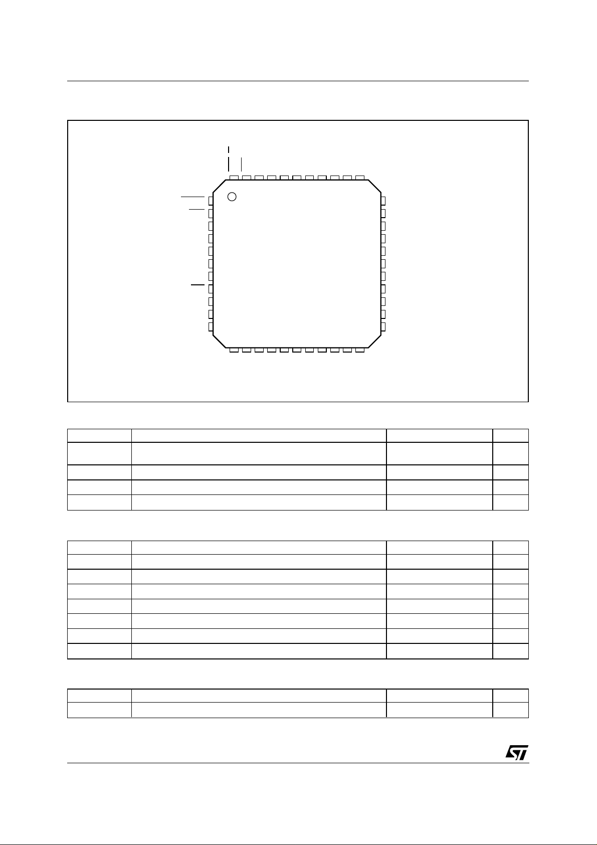
STLC30R80
PIN CONNECTION
CSOUT
CSIN
D0
D1
D2
N.C.
N.C.
RES
VDD
VCC
CRT
BGND
RING
TIP
AGND
AGND
AGND
DET
GDK/AL
44 43 42 41 3940 38 37 36 35 34
1
2
3
4
5
6
7
8
9
10
12 13 14 15 16
SW.
N.C.
N.C.
171118 19 20 21 22
TX
ZB
VBAT
AGND
RS
VREG
ZAC
BASE
CSVR
33
32
31
30
29
28
27
26
25
24
23
RX
PINCON_STLC30R80
ZAC1
CREV
IREF
RLIM
RTH
AGND
RT1
RT2
ILTF
RDC
CAC
TTXIN
ABSOLUTE MAXIMUM RATINGS
Symbol Parameter Value Unit
V
BAT
V
CC
V
DD
Battery voltage -80 + VCC to +0.4
-80 + V
REL
to + 0.4
Positive supply voltage -0.4 to +7 V
Control Interface Supply Voltage -0.4 to +7 V
A/R/BGND AGND respect BGND -2 to +2 V
OPERATING RANGE
Symbol Parameter Value Unit
T
opT
V
CC
V
DD
V
BAT
Operating temperature range -40 to +85 °C
Positive supply voltage 4.75 to 5.25 V
Control Interface Supply Voltage 3 to 5.25 V
Battery voltage -72 to -15 V
A/BGND AGND respect BGND -0.3 to +0.3 V
PD (70) Max. power dissipation @ Tamb = 70°C 1.1 W
PD(85) Max. power dissipation @ Tamb = 85°C 0.9 W
THERMAL DATA
Symbol Parameter Value Unit
R
th j-amb
Thermal resistance Junction to Ambient Typ. 60 °C/W
V
V
2/13
Page 3
STLC30R80
PIN DESCRIPTION
Pins Name Description
1
2
3 D0 Control Interface input bit 0. (*)
4 D1 Control Interface input bit 1. (*)
5 D2 Control Interface input bit 2. (*)
6 N.C. Not connected
7 N.C. Not connected
8
9V
10 V
11 CRT Ring-Trip time constant capacitor.
12 N.C. Not connected
13 N.C. Not connected
14 SW Internal switch/limiting current programming pin.
15 AGND Analog Ground
16 V
17 TX 4 wires output stage (Transmitting Port).
18 ZB Cancelling input of Balance Network for 2 to 4 wires conversion.
19 RS Protection resistors image. The image resistor is connected between this node and ZAC.
20 ZAC AC impedance synthesis.
21 ZAC1 RX buffer output/ AC impedance is connected between this node and ZAC.
22 RX 4 wires input stage (Receiving Port). A 100K external resistor must be connected to AGND to
23 TTXIN Metering Signal Input (AC) and Line Voltage Drop Programming (DC). If not used must be connectd
24 CAC AC feedback input/ AC-DC split capacitor is connected between this node and ILTF.
25 RDC DC current feedback input. The RDC resistor is connected between this node and ILTF.
26 ILTF Transversal Line Current Image.
27 RT2 Input pin to sense ringing current , for Ring-Trip detection.
28 RT1 Input pin to sense ringing current , for Ring-Trip detection.
29 AGND Analog ground.
30 RTH Off-Hook threshold programming pin.
31 RLIM Limiting current programming pin.
32 IREF Voltage reference output to generate internal reference current.
33 CREV Reverse polarity transition time programming.
34 CSVR Battery supply filter capacitor.
35 BASE Driver of the external transistor. Connected to the base.
36 VREG Regulated voltage. Provides the negative supply to the power line drivers. It is connected to the
37 BGND Battery ground.
38 RING B wire termination output. IB is the current sunk into this pin.
39 TIP A wire termination output. IA is the current sourced from this pin.
40 AGND Analog ground.
CSOUT Chip-Select for output control bits DET and GDK . Active Low. (*)
CSIN Chip-Select for input control bits latches D0 D1 D2 R0 R1 . Active Low. (*)
RES Reset Input; active low. After activation the SLIC is put in Power Down state
DD
CC
BAT
Control interface Power Supply. VDD = 3.3V or VDD = VCC.
Positive Power Supply (+5V).
Negative Battery Supply.
bias the input stage.
to AGND.
emitter of the external transistor.
3/13
Page 4
STLC30R80
CONTROL INTERFACE
INPUTS
D0 D1 D2
0
0
0
0
1
1
1
0
0
1
1
0
1
1
0/1
0
1
0
1
1
0
OPERATING MODE
Power down
Stand-by
Active N.P.
Active R.P.
Ringing
High Impedance Feeding
Ground Start
A parallel interface allow to control the operation
of STLC30R80 through a control bus:
- D0 D1 D2 latched input bits defining the Slic
operation mode
DET and GDK/AL , tri-state outputs, signal the
status of the loop: On/Off-Hook and Ground-Key.
GDK/AL goes low also when the device
Pin
thermal protection is activated or a line fault (Tip to
Ring, Tip and/or Ring to Ground or VBAT) is
detec ted (flowing c urren t ≥ 7.5mA).
CSIN: chip select for input bits, active Low,
strobes the data present on the control bus into
the internal latch.
CSOUT: c h i p s el ect for o u tpu t b it s ; a c tive L ow ,
when high DET and GDK/AL goes tri-state.
D0 D1 D2
CSIN and CSOUT inputs are provided
with a 15µA pull-down current to prevent uncontrolled conditions in case the control bus goes
floating.
According to the table 6 operating modes can be
set:
1) Power-Down.
2) Stand-By.
3) Active N.P.
4) Active R.P.
5) Ringing
6) High Impedance Feeding.
Power-Down
It’s an idle state characterised by a very low
power consumption; any functionality is disabled.
It can be set during out of service periods just to
reduce the power consumption.
It is worth noticing that two other conditions can
set the Slic in idle state but with some differences
as reported in the table:
Idle State DET GDK/AL
Power Down Disable Disable
Reset Disable Disable
Thermal Alarm Low Low
OUTPUTS
DET
(Active Low)
disable
off/hk
off/hk
off/hk
ring/trip
off/hk
off/hk
GDK/AL
(Active Low)
disable
gnd-key
gnd-key
gnd-key
disable
disable
gnd-key
Stand-By.
Mode selected in On-Hook condition when high
immunity to common mode currents is needed for
DET bit.
the
To reduce the current consumption, AC feedback
loop is disabled and only
DET and GDK/AL de-
tectors are a ct ive .
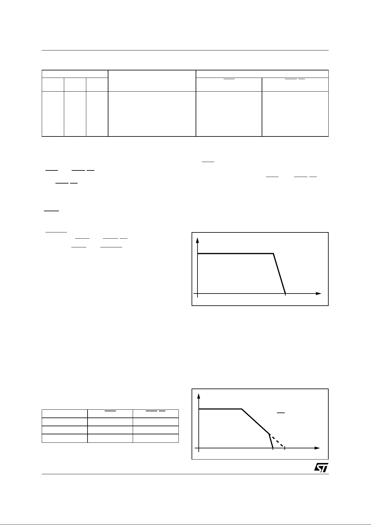
DC current is limited at 16mA (no t programma-
ble); feeding characteristic shown in fig. a.
The voltage drop in on-hook condition is 7.8V.
Figure a: STLC30R80 DC Characteristic in
Stand-By Mode.
I
16mA
R
= 2R
D98TL307
FEED
V
BAT
P
-7.8V
Active
Mode selected to allow voice signal transmission.
When in ACTIVE mode the voltage drop in onhook condition is 7.8V in order to allow proper onhook transmission (Fig. b).
Resistive Region is programmable by means of
external resistor R
lected by R
LIM
and R
, limiting current can be se-
DC
resistor.
switch
Figure b. STLC30R80 DC Characteristic in
Active M o de.
I
I
[20÷50mA]
LIM
D99TL435
R
FEED
R
= 2R
FEED
P
V
BAT
=
R
-7.8V
DC
+2R
P
5
V
BAT
V
V
4/13
Page 5

STLC30R80
Concerning AC characteristic the STLC30R80 allows to s et 2W termination impedanc e by means of
one exter nal scaled impedance t hat may be complex. Two to four wire conversion is provided by an
externa l network. Suc h network can be avoid ed in
case of application with COMBOII, in this case the
two to four wire conversion is implemented inside
the COMBOII by means of the programmable Hybal filte r.
When in ACTIVE mode it is also possible to perform battery reversal in soft mode (with programmable tra nsition time) witho ut affectin g the AC signal tran smi ss ion .
Ringing
When ringing mode is selected, by toggling the
D2 pin is possible to insert the ringing signal on
the line: the ringing frequency is equal to the one
applied to the D2 pin. The ringing s ignal is a balanced trapezoidal wave form where the TIP and
RING voltages switch continuously between GND
and VREG: VREG is obtained directly from VB1
(VREG = VB1 - 1.8V). The slope of the trapezoidal wave form is set by the external Crev capacitor and it allows to obtain ringing signal with distortion less than 10%: with a fine tuning of this
capacitor is possible to obtain distortion value
less than 5% (crest factor from 1.25 to 1.35).
Figure c. Typical ringing wave form.
As the ring trip is detected the logic indicator
DET
is set low and the ringing is automatically disconnected without waiting for the card controller command (auto ring trip).
Ringing with high REN number
When ringing high number of REN, for example
5REN, or short loops, it could happen that the line
AC current, trigger the ring trip circuit producing
false ring trip.
If this happens, a proper SW resistor (Rswitch)
can be inserted between RLIM and the pin.
The effect of this resistor is to improve the AC
current capability in Ring mode avoiding false ring
trip in presence of high REN numbers (typ.
5REN) and short loop.
One side effect of Rswitch is to reduce ring trip
sensitivity in presence of long loops; therefore it is
recommended to adjust Rswitch properly checking the correct behaviour of the dev ice in the two
worst-case conditions:
- 0Ω loop, Max REN#
- Max loop length, 1 REN
The lower is the Rswitch value; the higher is the
immunity to false Ring trip, producing as side effect a lower Ring trip sensitivity on long loops.
The typical value of Rswitch is s hown in the External Components Table (pag.7.13)
GND
VREG
TIP
RING
3V typ.
dV/dT set
by CREV
3V typ.
60V
typ.
The VB1 value must be higher enough (~70V) in
order to obtain ringing signals with more than
40Vrms. The VB2 battery is used only when the
line is in off hook and its value can be reduced
(typ. 24V) in order to minimize the power consumption.
The ring trip detection is performed sensing the
variation of the AC line impedance from on-hook
(relatively high) to off-hook (relatively low). This
particularly ring trip method allows to operate
without DC off-set superimposed on the ringing
signal and therefore obtaining the maximum possible ring level on the load star ting from a given
negative battery.
It should be noted t hat such a meted is optimized
for operation on short loop applications and may
not operate properly in presence of long loop
(>500 Ohm).
High Impedance Feeding.
As Stand-By, this mode is set in On-Hook condition, with further reduced power consumption.
Higher power efficiency turns back a lower immunity of the Off-Hook detector to line common
mode currents. The DC feeding shows a c onstant
current characteristic (I
= 17mA) followed by a
lim
resistive range with an equivalent series resistance R
= 1600Ω + 2Rp.
FEED
Thermal protection circuit is still active, preventing
the junction temperature, in case of fault condition, to exceed 150°C
In High Impedance Feeding most of the circuit is
switched off, only the circuit, dedicated to OffHook detection, is powered. This allows to reduce
Figure d. STLC30R80 DC Characteristic in
High Impedance Feeding
I
17mA
D98TL373
R
FEED
= 1600Ω +2R
V
BAT
P
-0.8V
V
5/13
Page 6

STLC30R80
Figure 1. Log ic Interface Input Timing
Min.
t1
t2
t3
t4
t5
t6
Note:
All measurements are performed with 100pF on outputs
pin and with TTL compatible voltage levels.
100ns
100ns
500ns
100ns
100ns
500ns
CSIN
D0.1.2
CSOUT
DET, GDK
t6t4 t5
t3t1 t2
Figure1_STLC30R80
the total power consumption in On-hook to 30mW
(typical).
The Off-Hook detection threshold is not progr ammable but defined at a fixed I
DETHI = 8mA(max .)
Ground Start.
This mode is selected when the SLIC is adopted
in a system using the Ground Start feature. In this
mode the TIP termination is set in High Impedance (100kΩ) while the RING one is active and
fixed at Vbat +4.8V. In the case of connection of
RING termination to GND the sinked current is
limited to 30mA. When RING is connected to
GND both Off-Hook and Ground-Key detectors
become active. Power dissipation in this mode
with a -48V battery voltage is 100mW.
PROTECTION CIRCUIT
Suggested protection circuit is based on programmable Trisils (like LCP1511/2) as shown in Fig.2
and Fig. 3, and the surge current is limited by the
resistors RPT2 and RPR2, which are PTC types ,
protecting the device against both lightning and
power-cross.
METERING PULSE INJECTION
STLC30R80 provides external pins and components for Metering Pulse injection. TTXIN pin is
the input for the 12kHz or 16kHz Metering Pulse
injection. This pin also provides a DC constant
current source that is injected into the external
RDA resistor (typ. 10kΩ) connected between
TTXIN pin and AGND. The voltage drop across
TIP and RING line amplifiers and, consequentally
the AC swing available.
When Metering Pulse injection is not used and
voltage drop is not required, TTXIN must be
shorted to AGND and RTTX, RDA and CTTX external components must be removed. The TTX
cancellation is obtained through an external
RTTX and CTTX network connected between
TTXIN and CAC pins
.
MISCELLANEOUS
- Thermal overload: the integrated thermal protection is activated when Tj reaches 150°C typ.;
the Slic is forced in Power-down mode,
DET
and AL are set Low.
- One low cost external transistor allows to reduce the power dissipated in the SLIC itself allowing the use of extreme small size package
(TQFP44). The external transistor size/package
can be selected depending on the max. power
requested by the particular application.
EXTERNAL COMPONEN TS LIST
To set the SLIC into operation the following parameters have to be defined:
- The DC feeding resistance "Rfeed" defined as
the resistance of the traditional feeding system (most common Rfeed values are: 400,
800, 1000 ohm).
- The AC SLIC impedance at line terminals "Zs"
to which the return loss measurements is referred. It can be real (typ. 600 ohm) or complex.
- The equivalent AC impedance of the line "Zl"
used for evaluation of the trans-hybrid loss performance (2/4wire conversion). It is usually a
complex impedance.
- The value of the two protection resistors Rp in
series with the line termination.
- The reverse polarity transition time defined as
/∆T".
"∆V
TR
- The constant current limit value "I
- Rth: sets the OFF/Hook
DETection threshold
lim
".
Once, the above parameters are defined, it is
possible to calculate all the external components
using the following table.
6/13
Page 7

EXTERNAL COMPONENTS
Name Function Formula Typical Value
(*) Internal current reference programming
R
REF
resistor
C
SVR
C
RT
R
DC
Battery ripple rejection capacitance
Ring Trip capacitance CRT = (25/fring) ⋅ 470nF 470nF ±20% 6V
DC sinthesized resistance
programming resistor
C
AC
R
S
AC/DC splitter capacitance
Protection resistor image RS = 25 ⋅ 2Rp 2.5kΩ ±1%
ZAC 2 wire AC impedance Z
1.16
I
=
REF
R
REF
C
=
SVR
RDC = 5[R
R
≥ 1kΩ
DC
C
=
AC
= 25[Zs - 2Rp] 12.5kΩ ±1%
AC
1
2π ⋅ fp ⋅ 1.3MΩ
-2Rp]
feed
1
2π ⋅ fsp ⋅ R
DC
ZA SLIC impedance balancing network ZA = 25 ⋅ Zs 15kΩ ±1%
ZB Line impedance balancing network ZB = 25 ⋅ Zl 15kΩ ±1%
C
COMP
AC feedback compensation
capacitance
C
COMP
=
2π ⋅ fo
2
[100
⋅ Rp]
RS1 Sensing resistor for Ring Trip 1000 ⋅ RR 600kΩ ±0.5%
RS2 Sensing resistor for Ring Trip 1000 ⋅ RR 600kΩ ±0.5%
Q
EXT
External transistor (1) BD140, MJD32
RPT1 Line series resistor ≥20Ω 20W 1/4W
RPR1 Line series resistor ≥20Ω 20Ω 1/4W ±1%
R
(*) Current limiting setting resistor
LIM
R
(***)
SWITCH
R
(**) OFF/HOOK DETection threshold
TH
Current limiting setting resistor
setting resistor.
C
REV
Polarity reversal transition time
programming
R
R
R
C
LIM
switch
TH
REV
= 200 ⋅
= 103 ⋅
[kΩ] =
K
=
∆V
1.16
; 26kΩ ÷ 64.9kΩ
I
LIM
Ω ⋅
24.4k
R
[kΩ] − 24.4kΩ
LIM
1.16
; 23.7kΩ ÷ 86.6kΩ
I
TH
1
K =
;
TR
3750
R
LIM
[kΩ]
∆T
RDA Output Voltage Drop Adjustment
R
TTX
C
TTX
Teletax Cancellation Resistor R
Teletax Cancellation Capacitor
∆Drop ⋅ 20k
RDA =
C
9.6
= 12.5 ⋅ [Re (ZL
TTX
=
TTX
12.5 ⋅ Im (ZL
(
− ∆Drop
Ω
) + 2RP]3.75kΩ
TTX
1
) ⋅ 2π ⋅
TTX
30.1kΩ ± 1%
100nF ±10% 100V
@ fp = 1.22Hz
@ 25Hz
1.5kΩ ±1%
10µF ±20% 15V
@ fsp = 10Hz
220pF ±20%
@ fo = 250kHz
51.1kΩ ±1%
47kΩ
26.1kΩ ±1%
47nF for 5.67V/ms
10kΩ (∆Drop = 3.2V) (2)
)
f
TTX
STLC30R80
RPT2 Protection resistor ≥ 8Ω
RPR2 Protection resistor ≥ 8Ω
D1 Overvoltage protection 1N4448
D2 Dual Battery Operation 1N4448
CH Trans-Hybrid Loss Frequency
CH = CCOMP 220pF ±30%
Compensation
C
VCC
C
VB
Notes:
(1) Transistor characteristics: h
For SMD application possible alternatives are MJD350 in D-PACK or BCP53 in SOT223
(2) Typical value needed for 2.2Vrms metering pulse level, if no metering RDA = 0Ω.
(*) R
REF
Avoid any digital line or high voltage swing line to pass close to I
(**) Inside the formula the coefficient 1.16 must be changed to 1.2 if the selected value of I
(***) This resistor must be used only in presence of REN number and short loop see description at page 5/13.
Power Supply Filter 100nF ±20%
Battery Supply Filter 100nF ±20% 100V
≥ 25, IC ≥ 100mA, V
FE
and RLIM should be connected close to the corresponding pins of STLC30R80.
≥ 60V, fT ≥ 15MHz. PDISS depends on application, see Appendix.
CEO
and R
REF
pins. Eventually screen these pins with a GND track.
LIM
is lower than 5mA.
Th
7/13
Page 8

STLC30R80
Figure 2. Typical application diagram.
V
V
CC
DD
To RSWITCH Resistor
D0
D1
D2
RDA RTTX
(1)
RX RX
TX
ZAZBCCOMP
CH
CONTROL
INTERFACE
GDK/AL GDK/AL
RES RES
(*) 1% match, 600KΩ typ.
(1) Components needed only for Metering pulse injection.
(2) to be inserted only for 5REN application
Figure 3. Test Circuit.
V
CAC
CAC
CC
RDC
ILTF
V
CC
CV
CC
ZAC1
RSZAC
ZAC
RS
TX
ZB
D0
D1
D2
DETDET
CSINCSIN
CSOUTCSOUT
TTXINTTX
CTTX
AGND BGND
V
DD
STLC30R80
CRT
RDC
CRT
V
DD
IREF
REF
RLIM
RLIM
SW
RTH
RSWITCH
(2)
TIP
RING
RT1
VREG
BASE
RS2(*)
RT2
VBAT
CSVR
CREV
RTH
From SWITCH PIN
To RSWITCH Resistor
RS1(*)
CREV
RPT1
VB1
RPR1
RPT2
LCP
1511
RPR2
D1
VB1
VB2
CSVR
TIP
RING
QEXT
D2
D99TL433CMod
220pF
8/13
CH
ZAC
12.5KΩ
ZA
CCOMP
15KΩ
220pF
ZB
15KΩ
CONTROL
INTERFACE
(*) 1% match, 600KΩ typ.
ZAC1
RTTX
3.75K
CTTX
1µF
ZAC
RS
RX
TX
ZB
D0
D1
D2
DETDET
CSINCSIN
CSOUTCSOUT
TTXIN
CAC
RS 2.5KΩ
RX
TX
D0
D1
D2
GDK/AL GDK/AL
RES RES
TTX
RDA
10K
CAC
10µF
ILTF
V
RDC
CC
1.5KΩ
V
DD
STLC30R80
CRT
RDC
AGND BGND
RREF
CRT
RREF
470nF
30.1KΩ
RLIM
51.1KΩ
RLIM
SW
RTH
RSWITCH
TIP
RING
RT1
VREG
BASE
RT2
VBAT
CSVR
CREV
RTH
26.1KΩ
RPT1 20Ω
VB-
RPR1 20Ω
RS1(*) 600KΩ
RS2(*) 600KΩ
CVB
CREV
47nF
From SWITCH PIN
LCP
1511
VB1 VB2
CSVR
100nF
RPT2 30Ω
RPR2 30Ω
QEXT
BD140
D1
1N4448
TIP
RING
D99TL434CMod
Page 9

STLC30R80
ELECTRICAL CHARACTERISTICS
= -48V, AGND = BGND, T
V
B-
= 25°C).
amb
(Test Condition, unless otherwise specified: V
= 5V, VDD = 3.3V,
CC
Note: the limits below listed are guaranteed with the s pecified test condition and in the 0 to 70°C temperature range. Performance over -40 to +85°C range are guaranteed by product characterisation.
Symbol Parameter Test Condition Min. Typ. Max. Unit Fig.
AC CHARACTERISTICS
Zil Long. Impedance each wire 40 Ω
I
il
L/T Long. to transv. with nominal Rp value 60 dB C5
T/L Transv. to long. 40 dB C3
2wRL 2W return loss. 300 to 3400Hz 22 dB C6
THL trans-hybrid loss. 1020Hz; 20Log |VRX/VTX| 30 dB C2
Ovl 2W overload level ACTIVE MODE at line
TXoff TX output offset -200 200 mV
G24 Transmit gain abs. 0dBm 1020Hz -12.38 -12.02 dB C4
G42 Receive gain abs. 0dBm 1020Hz 5.74 6.1 dB C1
G24fq tx gain variation vs.
G42fq rx gain variation vs.
V2wp idle channel noise at line
V4wp idle channel noise at TX port psophometric -90 -84 dBmp C7
Thd total harm. dist. 2w-4w, 4w-2w0dBm, 1KHz Il = 20 to
G
TTX
THD (TTX) TTX Harmonic Distortion 2.2V
DC CHARACTERISTICS (TTX pin connected to ground)
Vlohi Line voltage Il = 0, H.I. feeding 47 47.4 47.8 V
Vlo Line voltage Il = 0, SBY/ACTIVE/ON-
Ilims Short circ. curr. R
Ilimb Short circ. curr. R
Ilima Lim. current accuracy Rel to progr. val. 20 to 45mA
Rfeed Feed res. accuracy ACTIVE NP, RP -10 10 %
Rfeed H.I. Feeding resistance H.I. feeding 1100 2100 Ω
Long. Current Capability AC H.I. feeding per wire (ON-HOOK) 5 mApk
STANDBY or ACTIVE per
13 mApk
wire (ON-HOOK)
ACTIVE per wire (OFF-
HOOK). I
= Transversal
T
80 -I
T
mApk
Current
3.2 dBm
terminals on ref. imped.
frequency
frequency
rel. 1020Hz, 0dBm 300 to
3400Hz
rel. 1020Hz, 0dBm 300 to
3400Hz
-0.1 0.1 dB
-0.1 0.1 dB
psophometric -82 -78 dBmp C8
terminals
-50 dB
45mA
Transfer Gain V
TTX
G
TTX
with R
= 100mV
= 20Log
= 200Ω
L
= on 200Ω 3%
RMS
@ 16kHz
RMS
V
L
V
TTX
14.5 dB
38.6 39.9 40.6 V
HOOK
= 0, SBY 14 16 18 mA
loop
= 0, H.I. feeding 11 17 20 mA
loop
-10 10 %
ACTIVE NP, RP
9/13
Page 10

STLC30R80
ELECTRICAL CHARACTERISTICS
(continued)
Symbol Parameter Test Condition Min. Typ. Max. Unit Fig.
Ilact Feed current ACTIVE ACTIVE NP, RP
18 mA
Rloop = 1900Ω RDC = 1.5kΩ
Ilsby Feed current STBY STY, Rloop = 2.2KΩ
13 mA
RDC = 1.5kΩ
I
TIP
I
GS
I
DA
Tip Leackage Current Ground Start 1 µA
Ring Lead Current Ground Sart Ring to GND 33 mA
Reference current sourced
-60 µA
by TTX IN pin for Voltage
Drop programming
DETECTORS
I
det
Off-hook current threshold
ST-BY, ACTIVE
I
H.I. Off-Hook current threshold H.I. feeding 5 8 mA
det
Hys Off/On hook hyst. ST-BY, ACTIVE 15% I
Rel. to progr. val. 7 to 11mA -10 +10 %
Rel. to progr. val. 3 to 6mA -20 +20 %
det
mA
Td Dialling distortion ACTIVE -1 +1 ms
I
LL
I
gst
Ground Key Current
threshold
I
= IB - I
LL
A
Ground Start Detection
TIP to RING to GND or
RING to GND
I
= 2 ⋅ I
gst
det
7.5 mA
-10 +10 %
Threshold
DIGITAL INTERFACE
INPUTS: D0, D1, D2,
Vih Input high voltage V
Vil Input low voltage V
CSIN, CSOUT
= 3.3V 2 V
DD
= 3.3V 0.8 V
DD
Iih Input high current 30 µA
Iil Input low current 10 µA
OUTPUTS:
Vol Output low voltage Iol = 0.75mA;
Voh Output high voltage I oh = 0 .1 m A;
I
OZ
DET, GDK /AL
CSOUT = LOW 0.5 V
CSOUT = LOW 2.4 V
Tri-State Output Current CSOUT = High -10 +10 µA
POWER SUPPLY REJECTION
PSRRC V
to 2W port Vripple = 0.1Vrms
CC
27 dB C9
50 to 4000Hz
PSRRB Vbat to 2W port Vripple = 0.1Vrms
30 dB C9
50 to 4000Hz
POWER CONSUMPTION
I
I
I
CC
BAT
DD
VCC supply current H. I. Feeding On-Hook
SBY On Hook
ACTIVE On Hook
V
supply current H. I. Feeding On-Hook
BAT
SBY On Hook
ACTIVE On Hook
1.0
3.5
5.0
0.5
2.5
4.5
mA
mA
mA
mA
mA
mA
VDD Supply Current Any operating mode 100 320 µA
10/13
Page 11

STLC30R 8 0
APPENDIX A
Battery voltage autoset
The STLC30R80 shows a line voltage depending on the voltage applied to Vbat pin. In particular in the
On-Hook the line voltage is Vbat if the SLIC is put in HI-Z mode or Vbat -7.8V if the SLIC is put in Active
mode.
If the battery voltage applied to the Vbat pin is always -70V (necessary to generate the proper ringing
signal), during the On-Hook the line voltage is higher than 60V.
A simple circuit to generate the proper Off-Hook battery voltage can be used starting from the -70V as
shown in the below figure A1.
The RING command (active low) is used to switch on the NPN transistor and apply the battery voltage
directly to the Vbat pin. When the RING command is high the NPN transistor is off and the zener diode
reduces the voltage applied to the Vbat pin.
Figure A1.
V
CC
470KΩ
RING
47KΩ
68KΩ
D00TL461
BC556
BC558
470KΩ
24V
STLC30R80
V
BAT
BATTERY VOLTAGE (-70V)
11/13
Page 12

STLC30R80
DIM.
mm inch
MIN. TYP. MAX. MIN. TYP. MAX.
A 1.60 0.063
A1 0.05 0.15 0.002 0.006
A2 1.35 1.40 1.45 0.053 0.055 0.057
B 0.30 0.37 0.45 0.012 0.014 0.018
C 0.09 0.20 0.004 0.008
D 12.00 0.472
D1 10.00 0.394
D3 8.00 0.315
e 0.80 0.031
E 12.00 0.472
E1 10.00 0.394
E3 8.00 0.315
L 0.45 0.60 0.75 0.018 0.024 0.030
L1 1.00 0.039
K 0°(min.), 3.5˚(typ.), 7°(max.)
OUTLINE AND
MECHANICAL DATA
TQFP44 (10 x 10)
D
D1
A1
2333
34
B
44
1
e
11
TQFP4410
22
E
E1
12
L
0.10mm
.004
Seating Plane
B
K
A
A2
C
12/13
Page 13

STLC30R80
Information furnishe d is beli eved to be accu rate and reliable. However, STMicroelec tronics assumes no res ponsibility for the consequences
of use of such i nformation nor for any i nfringement of patents or ot her rights of third par ties which may result from its use. No license i s
granted by impli cation or otherwis e under any patent or patent righ ts of STMicroelect ronics. Specifica tion mentioned in this publication are
subject to change without notic e. This public ation supers edes and replaces all information prev iously supplied. STMic roelec tronic s products
are not authorized for use as critical components in life support devices or systems without express written approval of STMicroelectronics.
The ST logo is a registered trademark of STMicroelect roni cs
© 2001 STMicroelectronics – Printed in Italy – All Rights Reserved
STMicroelectronics GROUP OF COMPANIES
Australia - Brazil - Canada - China - Finland - France - Germany - Hong Kong - India - Israel - Italy - Japan - Malaysia - Malta - Morocco -
Singapore - Spain - Sweden - Switzerland - United Kingdom - United States.
http://www.st.com
13/13
 Loading...