

Page 1
SUBSCRIBER LINE INTERFACE CIRCUIT
MONOCHIP SLIC SUITABLE FOR PUBLIC
APPLICATIONS
IMPLEMENTES ALL KEY FEATURES OF
THE BORSHTFUNCTION
DUALCONTROL MODE CONFIGURATION:
SLAVE MODE OR AUTOMATIC ACTIVATION
MODE.
SOFT BATTERY REVERSAL WITH PROGRAMMABLETRANSITION TIME
ON HOOKTRANSMISSION
LOOP START/GROUND START FEATURE
WITH PROGR.THRESHOLD
LOW POWER DISSIPATION IN ALL OPER-
ATING MODES
AUTOMATIC DUAL BATTERY OPERATION
INTEGRATED RING TRIP DETECTION WITH
AUTOMATIC AND SYNCRONISED RING
DISCONNECTION
METERING PULSE INJECTION
SURFACEMOUNT PACKAGE
THREE RELAY DRIVERS FOR RING AND
TESTING
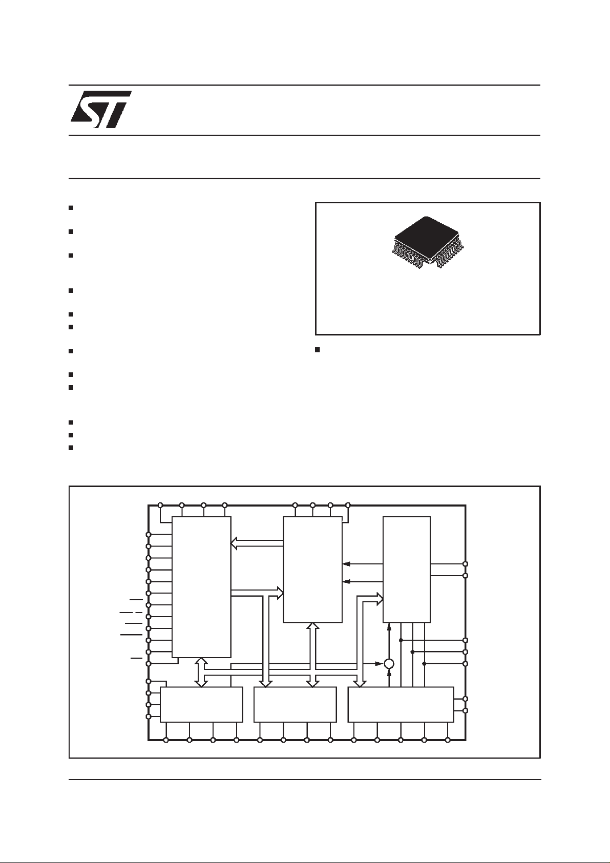
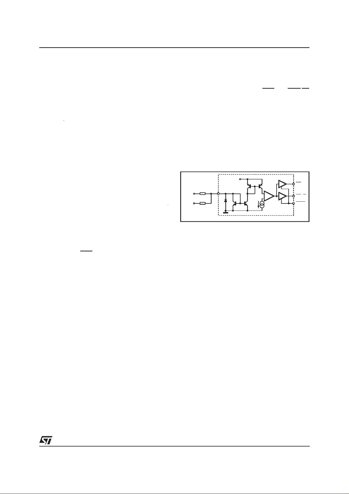
BLOCK DIAGRAM
STLC3080
PRELIMINARY DATA
TQFP44 (10 x 10)
ORDERING NUMBER: STLC3080
-40 TO +85°COPERATINGRANGE
DESCRIPTION
The STLC3080 is a SLIC device suitable for a
wide range of applications: public (CO), transmission (DLC) and private (PABX). The SLIC provides the standard battery feeding with full programmability of theDC characteristic.In particular
two external resistors allow to set the limiting current value (up to 50mA) and the value of the resistive feeding when not in constant current region.
REL1
RELRREL0
MODE
D0
D1
D2
R0
R1
DET
GDK/AL
CSIN
CSOUT
CKRING
RES
TTXIN
ZB
TX
RX
ZAC1
LOGIC
INTERFACE
&
DECODER
AC
PROCESSOR
RSZAC IREF V
RGND
LINE STATUS
COMMANDS
REFERENCE
BIAS SWITCHING
CAC AGND CREV CSVR
RT1 RT2CRT
SUPERVISION
&
V
CC
DD
PCD
ILT
ILL
AC+
DC
AC
DC
December 1999
This is preliminary information on a new product now indevelopment or undergoing evaluation.
LINE
INTERFACE
+
DC
PROCESSOR
VBAT BASE RDC
TIP
RING
BGND
VREG
ILTF
RLIM
RTH
D98TL305B
1/23
Page 2
STLC3080
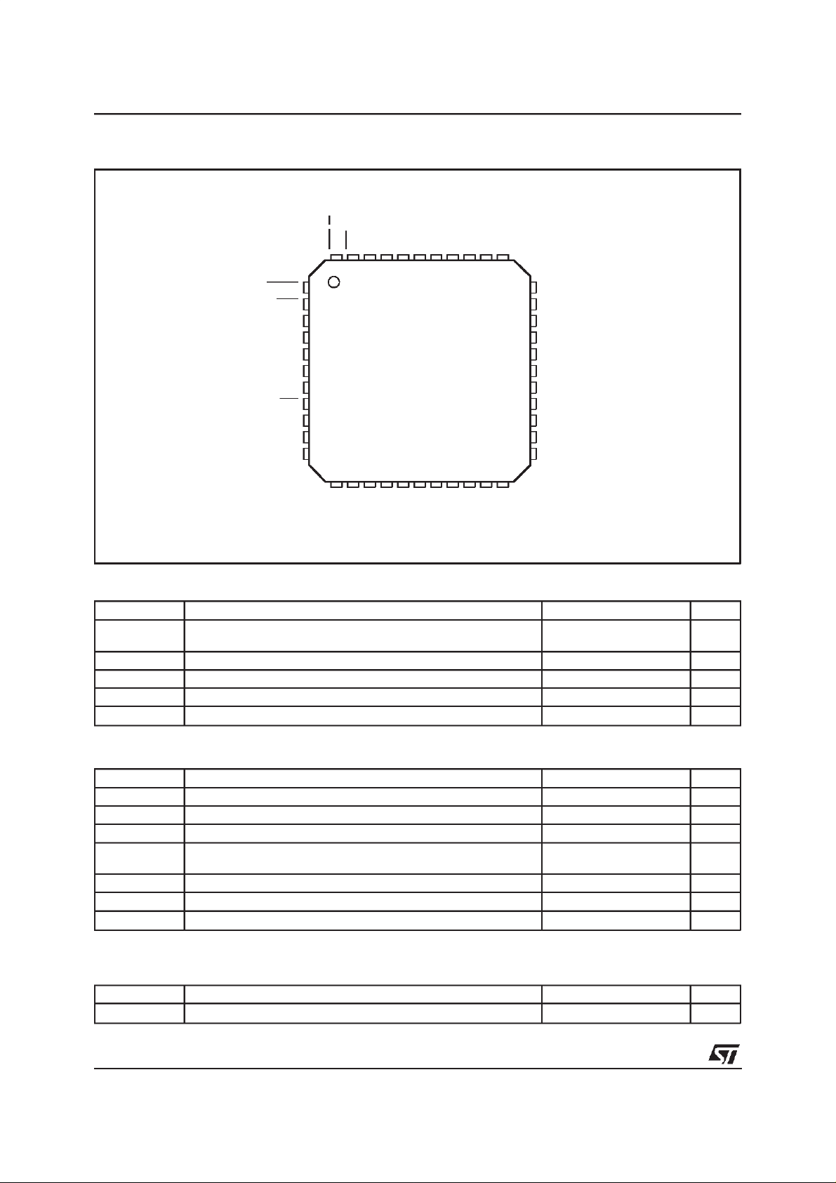
PIN CONNECTION
CSOUT
CSIN
D0
D1
D2
R0
R1
RES
VDD
VCC
CRT
BGND
RING
TIP
PCD
MODE
CKRING
DET
GDK/AL
44 43 42 41 3940 38 37 36 35 34
1
2
3
4
5
6
7
8
9
10
RELR
RGND
VBAT
171118 19 20 21 22
TX
ZB
RS
12 13 14 15 16
REL1
REL0
VREG
ZAC
BASE
ZAC1
CSVR
33
32
31
30
29
28
27
26
25
24
23
RX
CREV
IREF
RLIM
RTH
AGND
RT1
RT2
ILTF
RDC
CAC
TTXIN
D98TL306A
ABSOLUTE MAXIMUM RATINGS
Symbol Parameter Value Unit
V
V
V
I
BAT
CC
DD
REL
Battery voltage -80 + VCCto +0.4
-80 + V
REL
to + 0.4
Positive supply voltage -0.4 to +7 V
Control Interface Supply Voltage -0.4 to +7 V
Current into relay drivers 80 mA
A/R/BGND AGND respect BGND respect RGND -2 to +2 V
OPERATINGRANGE
Symbol Parameter Value Unit
T
opT
V
CC
V
DD
V
BAT
Operating temperature range -40 to +85 °C
Positive supply voltage 4.75 to 5.25 V
Control Interface Supply Voltage 3 to 5.25 V
Battery voltage
if VREL > V
CC
-73 to -15
-78+ V
REL
to -15
A/R/BGND AGND respect BGND respect RGND -0.3 to +0.3 V
PD (70) Max. power dissipation @ Tamb = 70°C 1.1 W
PD(85) Max. power dissipation @ Tamb = 85°C 0.9 W
THERMAL DATA
V
V
V
V
Symbol Parameter Value Unit
R
th j-amb
Thermal resistance Junction to Ambient Typ. 60 °C/W
2/23
Page 3

STLC3080
PIN DESCRIPTION
Pins Name Description
1 CSOUT Chip-Select for output control bits DET and GDK . Active Low. (*)
2 CSIN Chip-Select for input control bits latches D0 D1 D2 R0 R1 . Active Low. (*)
3 D0 Control Interface inputbit 0. (*)
4 D1 Control Interface inputbit 1. (*)
5 D2 Control Interface inputbit 2. (*)
6 R0 Relay driver 0 command. Active High. (*)
7 R1 Relay driver 1 command. Active High. (*)
8 RES Reset Input; active low.
9V
10 V
DD
CC
11 CRT Ring-Triptime constant capacitor.
12 REL1 Relay 1 driver output.
13 REL0 Relay 0 driver output.
14 RELR Ringer Relay driver output.
15 RGND Relay drivers ground.
16 V
BAT
17 TX 4 wires outputstage (Transmitting Port).
18 ZB Cancelling input of Balance Network for 2 to 4 wires conversion.
19 RS Protection resistors image. The image resistor is connected between this node and ZAC.
20 ZAC AC impedance synthesis.
21 ZAC1 RX buffer output/ AC impedance is connected between this node and ZAC.
22 RX 4 wires inputstage (Receiving Port). A 100K externalresistor must be connected to AGND to
23 TTXIN Metering SignalInput (AC) andLine Voltage DropProgramming(DC). If notusedmustbe connectd
24 CAC AC feedback input/ AC-DC split capacitor is connected between this node and ILTF.
25 RDC DC current feedback input. The RDC resistor is connected between this node and ILTF.
26 ILTF TransversalLine Current Image.
27 RT2 Input pin to sense ringing current , for Ring-Trip detection.
28 RT1 Input pin to sense ringing current , for Ring-Trip detection.
29 AGND Analog ground.
30 RTH Off-Hook threshold programming pin.
31 RLIM Limiting current programming pin.
32 IREF Voltage reference output to generate internal reference current.
33 CREV Reverse polarity transition time programming.
34 CSVR Battery supply filter capacitor.
35 BASE Driver ofthe external transistor. Connected to the base.
36 VREG Regulated voltage. Provides the negative supply to the power line drivers. It is connectedto the
37 BGND Battery ground.
38 RING B wire termination output. IB is the current sunk into this pin.
39 TIP A wire termination output. IA is the current sourced from this pin.
40 PCD Power Cross Detection Input
41 MODE InterfaceControl Mode selection.
42 CKRING Clock at ringing frequency for relay synch and time reference for Automatic activation
43 DET Off-hook and Ring-Trip detection bit. Tri-State Output/Active Low.
44 GDK/ AL Ground-Key/Alarm detection bit. Tri-State Output. Active Low.
* Input pins provided with 15µA sink toAGND pull-down.
Control interface Power Supply. VDD= 3.3V orVDD=VCC.
Positive Power Supply (+5V).
Negative Battery Supply.
bias the input stage.
toAGND.
emitter of the external transistor.
3/23
Page 4
STLC3080
CONTROLINTERFACE
Slave mode (MODE=Low).
INPUTS
R0 R1 D0 D1 D2
X
X
X
X
X
X
X
X
0/1
X
X
X
X
X
X
X
X
X
X
0/1
0
0
0
0
1
1
1
1
X
X
0
0
1
1
0
0
1
1
X
X
X
X
0
1
0
1
0
1
0
1
OPERATING MODE
Power down
Stand-by
Active N.P.
Active R.P.
Ringing (with SLIC Active N.P.)
Ringing (with SLIC Active R.P.)
Ground start
High Impedance Feeding
Rel 0 (on = 1, off = 0)
Rel 1 (on = 1, off = 0)
A parallel interface allow to control the operation
of STLC3080through a control bus:
- D0 D1 D2 latched input bits definingtheSlic
operationmode
- R0 R1 latched input bits (activeHigh) drive the
testrelays.
- DET and GDK/AL , tri-state outputs, signal the
statusofthe loop:On/Off-Hookand Ground-Key.
PinGDK/AL goeslow also whenthe device
thermal protectionis activatedor a linefault(Tip to
Ring,Tip and/orRingto Groundor VBAT)is
detected(flowing current≥7.5mA).
-CSIN: chipselect for input bits, active Low,
strobesthe data present on the control bus into
theinternal latch.
- CSOUT: chipselect for outputbits; activeLow,
whenhigh DET and GDK/AL goes tri-state.
D0 D1 D2 R0 R1 CSIN and CSOUT inputsare
provided with a 15µA pull-down current to prevent
uncontrolled conditions in case the control bus
goes floating.
According to theabove table, 8 operating modes
can be set:
1) Power-Down.
2) Stand-By.
3) ActiveN.P.
4) ActiveR.P.
5) Ringing(with SLIC Active N.P.).
6) Ringing(with SLIC Active R.P.).
7) Groundstart.
8) HighImpedanceFeeding.
Power-Down
It’s an idle state characterised by a very low
power consumption; any functionalityis disabled;
only relays Rel0 and Rel1 can be driven by
proper settingof bitsR0 and R1.
It can be set during out of service periods just to
OUTPUTS
DET
(Active Low)
disable
off/hk
off/hk
off/hk
ring/trip
ring/trip
off/hk
off/hk
def by D0-D2
def by D0-D2
GDK/AL
(Active Low)
disable
gnd-key
gnd-key
gnd-key
disable
disable
gnd-key
disable
def by D0-D2
def by D0-D2
reducethe power consumption.
It is worth noticing that two other conditions can
set the Slic in idle state but with somedifferences
as reportedin the table:
Idle State Rel0/1 Drive DET GDK/AL
Power Down Enable Disable Disable
Reset Disable Disable Disable
Thermal
Alarm
Enable Low Low
Stand-By.
Mode selected in On-Hook condition when high
immunity to common mode currents is needed for
the DET bit.
To reducethe current consumption, AC feedback
loop is disabled and only DET and GDK/AL detectorsare active.
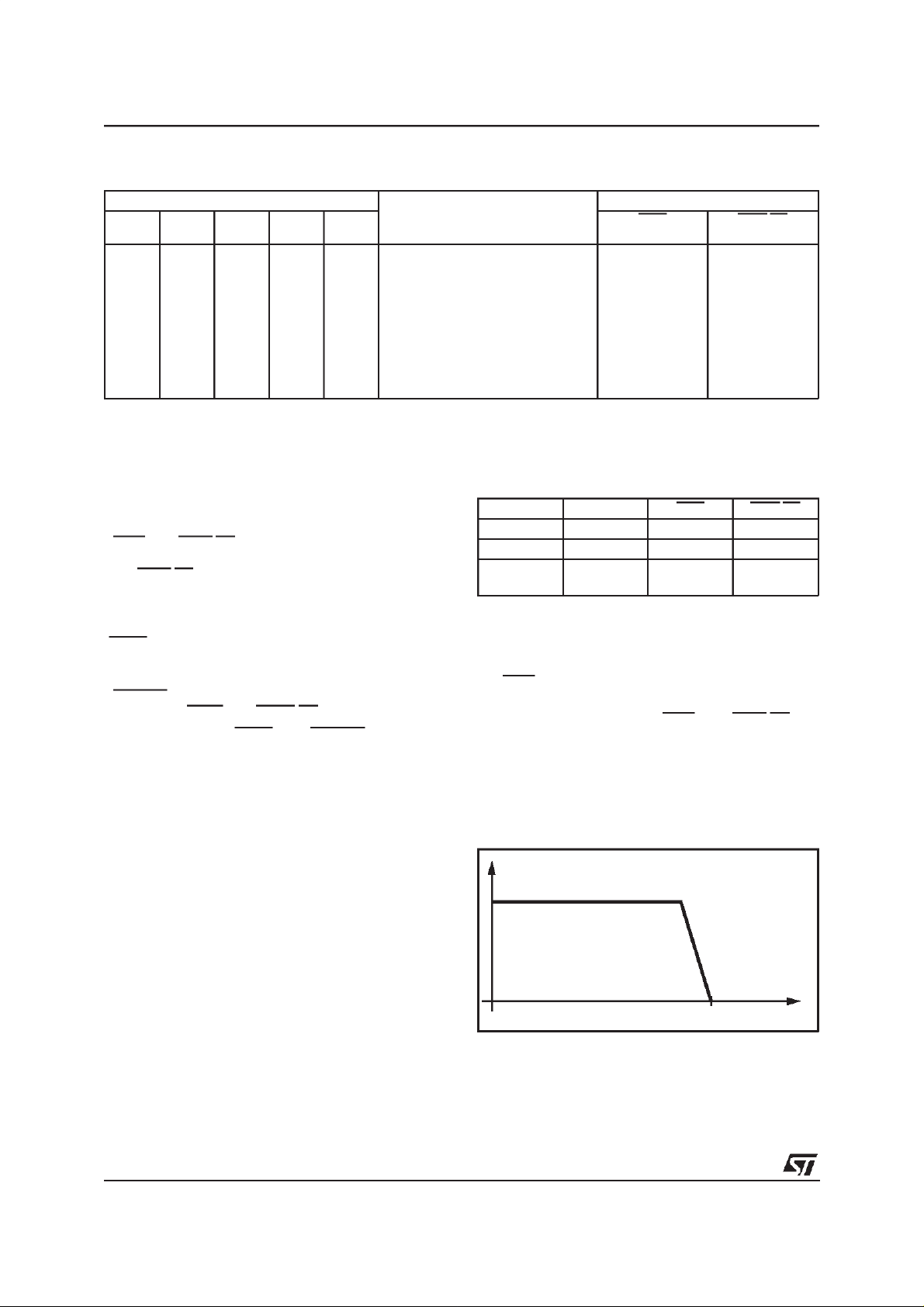
DC current is limited at 16mA (not programmable); feedingcharacteristicshown in fig.a.
The voltage drop in on-hook conditionis 7.8V.
Figurea: STLC3080 DC Characteristicin
Stand-ByMode.
I
16mA
R
=2R
D98TL307
FEED
V
BAT
-7.8V
P
V
Active
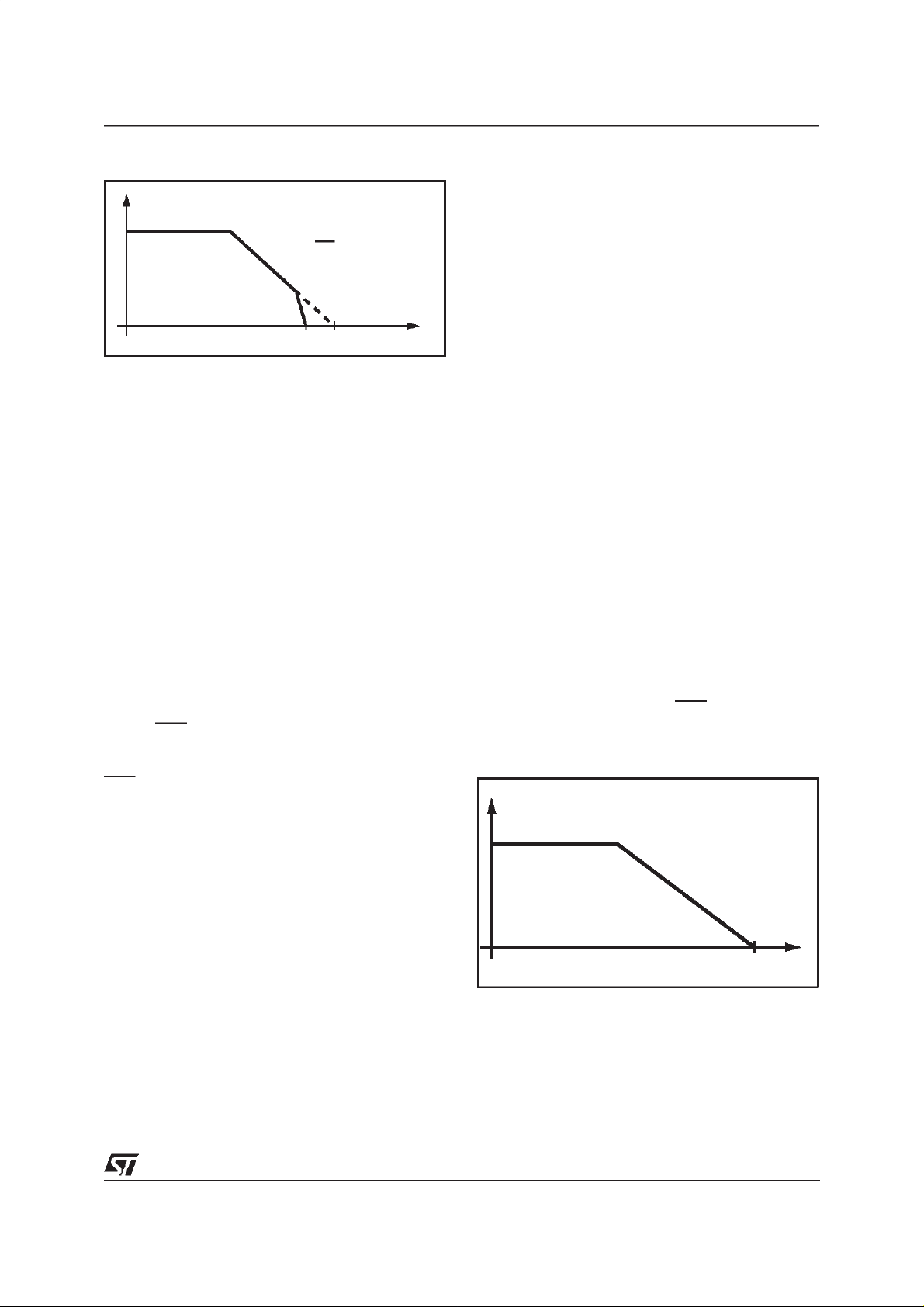
Mode selected to allow voice signal transmission.
When in ACTIVE mode the voltage drop in onhook condition is 7.8Vin orderto allowproper onhook transmission(Fig. b).
4/23
Page 5
STLC3080
Figure b. STLC3080DC Characteristicin
ActiveMode.
I
I
[20÷50mA]
LIM
R
R
=2R
FEED
FEED
V
P
BAT
=
-7.8V
R
DC
+2R
P
5
V
BAT
V
Resistive Region is programmable by means of
external resistor R
lected by R
LIM
, limiting current can be se-
DC
resistor.
Concerning AC characteristic the STLC3080 allows
to set 2W terminationimpedance by meansof one
external scaled impedance that may be complex.
Two to four wire conversion isprovidedby an external network.Such network can be avoidedin case
of applicationwith COMBOII,in this casethe two to
four wire conversion is implemented inside the
COMBOII by means of the programmableHybal filter.
When in ACTIVE mode it is also possible to perform battery reversal in soft mode (with programmable transition time) without affectingthe AC signaltransmission.
Ringing
When Ringing mode is selected the STLC3080
activates the ring relay injectingthe ringing signal
on the line. As the ring trip is detectedthe logic indicator DET is set low and the ringing is automatically disconnected without waiting for the card
controllercommand (auto ring trip).
DET remains latched Low untill the operative
mode is modified.
If required , the ringing relay drive signal RELR
can be synchronised to a clock applied to
CKRINGinput.
This clock is derived from the ringing signal with
proper time delay, according to the activation/deactivationtime of the relay.
RELR is activated on the low level of CKRING
clock. The duty cycleof CKRING can be modified
in order to activate the RELR when required:
CKRINGlow must last 1µs minimum.
If the synchronisation is not required, CKRING input must be steadily kept Low.
All the STLC3080 relay drivers are open drain
with the source connectedto theRGND pin. Each
relay drivers integrates a protection structure that
allows to avoid external kick - back diodes,using
both 5Vor 12V relays.
The ring trip circuit and its behaviour is described
in AppendixD.
Ground Start.
This mode is selected when the SLIC is adopted
in a system using the Ground Start feature. In this
mode the TIP termination is set in High Impedance (100kΩ) while the RING one is active and
fixed at Vbat +4.8V. In the case of connection of
RING termination to GND the sinked current is
limited to 30mA. When RING is connected to
GND both Off-Hook and Ground-Key detectors
become active. Power dissipation in this mode
with a -48Vbattery voltage is 100mW
High Impedance Feeding.
As Stand-By, this mode is set in On-Hook condition, with furtherreducedpower consumption.
Higher power efficiency turns back a lower immunity of the Off-Hook detector to line common
modecurrents.
The DC feeding shows a constant current characteristic (I
with an equivalent series resistance R
= 17mA) followed by a resistive range
lim
FEED
1600Ω+ 2Rp.
Thermal protection circuit is still active, preventing
the junction temperature, in case of fault condition, to exceed150°C
In High Impedance Feeding most of the circuit is
switched off, only the circuit, dedicated to OffHook detection, is powered. This allows to reduce
the total power consumptionin On-hookto 30mW
(typical).
The Off-Hook detection threshold is not programmablebut defined at a fixed IDET
= 8mA(max.)
HI
Figurec. STLC3080 DC Characteristicin High
ImpedanceFeeding
I
17mA
D98TL373
R
FEED
= 1600Ω +2R
V
BAT
P
-0.8V
=
V
5/23
Page 6

STLC3080
CONTROLINTERFACE
Automatic activation mode (MODE=High).
Inputs Operating Mode
R0 R1 D0 D1 D2
X X 0 0 0 1 Power Down disable disable
X X 0 0 1 1 Ringing Ring-Trip disable
X X 0 1 0 1 On-Hook Transmission
X X 0 1 1 1 On-Hook Transmission
X X 1 0 0 1 Active Direct Polarity
X X 1 0 1 1 Active Direct Polarity
X X 1 1 0 1 Active Reverse Polarity Off_Hook
X X 1 1 1 1 Active Direct Polarity
0/1 X X X X 1 R0 = 0/1: Rel0 = off/on (1) (1)
X 0/1 X X X 1 R1 = 0/1: Rel1 = off/on (1) (1)
XXXXX0Power Down; Rel0/1= off disable disable
DET: On/OffHook Signalling; togetherwith GDK/AL it is set Low also in case of Thermal Alarm or Ground-Key.
GDK/AL : Thermal Alarm or Ground-Key Signalling
(1) : DET and GDK/AL signallingfunction is relatedto D0,D1,D2 and it doesn’t depend on R0 and R1 setting.
RES DET GDK/AL
As in Slave mode the control is performed
through a parallel bus, with independent chip selects, CSIN and CSOUT, for inputs and outputs.
In Automatic Activation, once Active mode is selected the device automatically selects the proper
operating mode (Active,Stand By or H.I. feeding)
depending on the loop status in order to optimise
the power consumption.
In order to guaranteethe proper behaviour of the
internal state machine the ”CKRING” signal must
be always applied,this signalin fact is used to generatethe ”WTIME” delay(see Appendix)necessary
to properlyperformautomaticstatechange.
Power-Down
It’s an idle state characterised by a very low
power consumption; any functionalityis disabled;
only relays Rel0 and Rel1 can be driven by
proper settingof bitsR0 and R1.
It can be set during out of service periods just to
reduce the power consumption.
(Mode = High)
Off-Hook
Reverse Polarity
Off_Hook
Direct Polarity
Off_Hook
(default)
Off_Hook
(default)
Off_Hook
(default)
As a Ring-Trip is detected the logic indicator DET
is set Low and the ringing relay is automatically
switched-off without waiting for the card controller command(auto ring-trip).
DET remains latched Low until the operative
modeis modified.
Ringingrelay drive signal RELR must be synchronised to a clock applied to CKRING input. This
clock is derived from the ringing signal with
proper time delay, according to the activation /
deactivationtime of the relay.
RELR is activated on the low level of CKRING
clock. The duty cycle of CKRING can be modified
in order to activate the RELR when required:
CKRINGlow must last 1µs minimum.
All the relay drivers are open-drain with the
sourceconnectedto RGNDpin.
Each relay driver integrates a protectionstructure
to avoid external kick-back diodes using both 5V
or 12V relays.
The ring trip circuit and its behaviouris described
in AppendixD.
Outputs
Fault
Fault
Fault
Fault
Fault
Fault
It is worth noticing that two other conditions can
set theSlic in idle state but with some differences
as reported in the table:
Idle State Rel0/1 Drive DET GDK/AL
Power Down Enable Disable Disable
Reset Disable Disable Disable
Thermal
Alarm
Enable Low Low
On-HookTransmission.
Sets the Slic for conversation even thoughthe line
is in On-Hook; it is required for On/Hooktransmission purposes; Active mode cannot supporta conversationwhenthe lineis in On-Hookasit automatically turns in High ImpedanceFeeding.
Active.
Ringing
When Ringing mode is selected the STLC3080
activatesthe ringing relay injecting the ringing signal on the line.
6/23
The relevant feature of this setting is that when
Active Mode (D0D1D2=1XX) is set by the external control , internally, the device is ableto select
between three operative states according to the
statusof the line:
Fault
Fault
Fault
Fault
Fault
Fault
Page 7
STLC3080
- High Impedance Feeding :
entered aftera Power-On Resetor 1XX word, this
statusis setduringsteadyOn/Hookcondition;
most of the circuitry is idle and only a low power
Off-Hookdetection circuit iskept alive.
Direct Polarity only is assumed , independentlyof
the selectedone.
To minimisethepowerconsumptiontheOff-Hookde-
tectioncircuithaslowcommonmodecurrentrejection.
-Standby
Notice that in Stand-Bystate theOff-Hook detec-
tor is sensitive only to the transversal component
of the line current with high immunity to common
mode disturbances; this performance implies an
increasing in power consumption: for that reason
Stand-Byis notused as a quiescent state.
- Active state gets operative for conversation after an Off-Hook validity check performed in
Stand-Bystate, set after any Off-Hook detected in
High ImpedanceFeeding.
If the Off-Hook condition is confirmedin StandBy,
Active mode is set ; if not (in case of spuriousdetection), false activation is prevented, and High
ImpedanceFeeding is resumed.
In order to havethe device falling back in HI-feeding mode after the line is back in on-hook condition. It is necessaryto selectas input state the active direct polarity mode (default).
During Active state On/Off-Hook status will affect in real time DET signalling bit.
In order to allow Pulse-Mode Dialling, once Active state is set, it cannot be changed by fast OnHook , but it is turned back to High Impedance
Feeding only if an On-Hook condition lasts
longer than 128 x CKRING period.
Automatic activation (and deactivation) is based
on an internal state-machine which is clocked by
a freerunninginternal oscillator.
A detaileddescriptionis reportedin the AppendixA.
DUAL BATTERY CONFIGURATION
STLC3080 is also meant for low power consumption systems using Dual Battery solution. It is sufficient to connectthe collector of the external transistor, through a diode, to the reduced battery
(see Fig. 2 for single battery solution and Fig. 3
for dual battery solution). The activation of the
batteries is automatic, only depending on the DC
load at the RING and TIP terminals; no controllers
action is required.
PROTECTIONCIRCUIT
- Suggested protection circuit is based on programmable Trisils (like LCP1511/2) as shown
in Fig.2 and Fig. 3, and the surge current is
limited by the resistors RPT2 and RPR2, which
are PTC types , protecting the device against
both lightningand power-cross.
- Additionally, STLC3080 is provided with the
PCD input to directly monitor overvoltages applied to the line wires.
When the current injected into PCD exceeds a
threshold of 320µA (+/- 30%) , DET and GDK/AL
are set Low signalling a fault condition. No
change on theSLIC mode is performed.
Voltage threshold is defined by proper value of
the series resistors (see Fig.1)
This circuit gives the possibility to protect the device against power crosses through a relay instead of PTCs; once the fault condition is detected the controller drives this relay
disconnectingthe Slic from the line terminals.
METERINGPULSE INJECTION
Figure1.
TIP
RING
VCC
R
PCD
R
Ith
DET
GDK/AL
CSOUT
D98TL385
STLC3080 provides external pins and components for Metering Pulse injection. TTXIN pin is
the input for the 12kHz or 16kHz Metering Pulse
injection. This pin also provides a DC constant
current source that is injected into the external
RDA resistor (typ. 10kΩ to obtain 2.2Vrms on
200Ω) connected between TTXIN pin and AGND.
The voltage drop across TIP and RING line amplifiers and, consequentallythe AC swing available.
When Metering Pulse injection is not used and
voltage drop is not required, TTXIN must be
shorted to AGND and RTTX, RDA and CTTX external components must be removed. The TTX
cancellation is obtained through an external
RTTX and CTTX network connected between
TTXIN and CAC pins.
Fault detection
The device provides current sense on TIP and
RING wires that allow to detect longitudinal DC
current (I
). When this ILLcurrent becomes
LL
higher than a threshold (see detectors table inside electrical characteristics) a fault indication is
provided on DET and GDK pin (both outputs become low). The fault indication is active till the
fault cause persists. With this circuit the following
fault condition can be detected.
TIP to VB1
TIP to GND
RINGto VB1
RINGto GND
RINGto TIP to VB1
7/23
Page 8

STLC3080
When a fault is detected the line current is limited
in order to avoid any damage on the device itself
and also on the external transistor.
EXTERNALCOMPONENTS LIST
To set the SLIC into operation the following parametershave to be defined:
- The DC feeding resistance”Rfeed” defined as
MISCELLANEOUS
- Thermal overload: the integrated thermal protectionis activated when Tj reaches150°C typ.;
the Slic is forced in Power-down mode, DET
and AL are set Low. The RELR relay driver is
turned off while it is still possible to control
REL0and REL1throughR0 andR1 inputs.
- One low cost external transistor allows to reduce the power dissipatedin the SLIC itself allowing the use of extreme small size package
(TQFP44).The external transistor size/package
can be selected depending on the max. power
requestedby the particularapplication.
- The SLIC supports loop start lines and gives
the possibility to set loop current indicator
thresholdby means of one external resistor.
the resistance of the traditional feeding system (most common Rfeed values are: 400,
800, 1000 ohm).
- The AC SLIC impedanceat line terminals ”Zs”
to which the return loss measurements is referred. It can be real (typ. 600 ohm) or complex.
- The equivalent AC impedance of the line ”Zl”
used for evaluation of the trans-hybrid loss
performance (2/4wire conversion). It can be a
compleximpedance.
- The value of the two protectionresistors Rp in
series with the line termination.
- The reverse polarity transition time defined as
/∆T”.
”∆V
TR
- The constantcurrentlimit value”I
- Rth: sets the OFF/HookDETection threshold
Once, the above parameters are defined, it is
possible to calculate all the external components
using the followingtable.
EXTERNAL COMPONENTS
Name Function Formula Typical Value
CVCC Positive Supply Filter 100nF ±20%
CVB Battery Supply Filter 100nF ±20% 100V
(*) Internal current reference
R
REF
C
SVR
C
RT
R
DC
C
AC
R
S
ZAC 2 wire AC impedance Z
ZA SLIC impedance balancing network ZA = 25⋅Zs 15k
ZB Line impedance balancing network ZB = 25⋅Zl 15k
C
COMP
RR Feeding resistance for Ring Injection
RS1 Sensingresistor for Ring Trip 1000 ⋅ RR 600kΩ ±1%
RS2 Sensingresistor for Ring Trip 1000 ⋅ RR 600kΩ ±1%
RT Feeding resistancefor Ring Injection ≥0Ω 0Ω
Q
EXT
RPT1 Line series resistor ≥20
RPR1 Line series resistor ≥20
programming resistor
Battery ripple rejection capacitance
Ring Trip capacitance see Appendix D 470nF±20% 6V
DC sinthesized resistance
programming resistor
AC/DC splitter capacitance
Protection resistor image RS=25⋅2Rp 2.5kΩ ±1%
AC feedback compensation
capacitance
External transistor (1) BD140
1.16
I
=
REF
R
REF
2π
⋅ fp ⋅ 1.3MΩ
feed
2
fsp⋅R
π ⋅
=
2π ⋅ fo
1
1
-2Rp]
2
[100
DC
⋅ Rp]
=
C
SVR
RDC= 5[R
R
≥ 1kΩ
DC
C
=
AC
= 25[Zs - 2Rp] 12.5k
AC
C
COMP
400
≥
Ω
Ω
Ω
30.1kΩ ± 1%
100nF ±10% 100V
@ fp = 1.22Hz
@ 25Hz
1.5kΩ ±1%
10µF ±20% 15V
@ fsp = 10Hz
1%
Ω ±
1%
Ω ±
1%
Ω ±
220pF±20%
@ fo = 250kHz
600Ω2W
20Ω 1/4W ±1%
lim
”.
8/23
Page 9

STLC3080
EXTERNAL COMPONENTS
(continued)
Name Function Formula Typical Value
(*) Current limiting setting resistor
R
LIM
= 103⋅
1.16
I
LIM
R
LIM
51.1k
Ω ±
23.2kΩ ÷ 58kΩ
R
(**) OFF/HOOK DETection threshold
TH
setting resistor.
R
TH
=200 ⋅
1.16
I
TH
26.1k
Ω ±
21.1kΩ ÷ 77.3kΩ
C
REV
RDA OutputVoltageDropAdjustment
Polarity reversal transition time
programming
C
REV
RDA
K
=
∆V
TR
T
∆
∆Drop⋅ 20k
=
9.6
−∆Drop
;K=
3750
Ω
1
47nF for5.67V/ms
10kΩ (∆Drop = 3.2V) (2)
R1, R2 Power Cross Detection 240kΩ (3)
R
TTX
C
TTX
Teletax Cancellation Resistor R
Teletax Cancellation Capacitor
= 12.5 ⋅ [Re (ZL
TTX
=
C
TTX
12.5⋅I
(
)+2RP] 3.75kΩ
TTX
1
ZL
(
TTX
)⋅2π ⋅ f
m
20Ω 1/4W ±1%
)
TTX
RPT2 Protection resistor ≥ 8Ω
RPR2 Protection resistor ≥ 8Ω
D1 Overvoltage protection 1N4448
D2 Dual Battery Operation 1N4448
CH Trans-Hybrid Loss Frequency
CH = CCOMP 220pF ±30%
Compensation
1%
1%
Notes:
(1) Transistorcharacteristics: h
For SMD applicationpossible alternatives are MJD350 in D-PACKor BCP53 in SOT223
(2) Typicalvalue needed for 2.2Vrms metering pulse level, if no metering RDA = 0Ω.
(3) These resistors are needed to activate the power cross detection circuit, they should withstand the typical lighting voltage. If the power
cross detection is not needed R1, R2 can be avoided.
andRLIM should be connected close to the corresponding pins of STLC3080.
(*) R
REF
Avoid any digital line or high voltage swing line to pass close to I
(**) Inside the formula the coefficient 1.16 must be changed to 1.20 if theselected value of I
≥ 25, IC≥ 100mA, V
FE
≥ 60V, fT≥ 15MHz. PDISS depends on application,see Appendix.
CEO
REF
and R
pins. Eventuallyscreen these pins with a GND track.
LIM
islower than 5mA.
th
9/23
Page 10

STLC3080
Figure 2. Typicalapplicationdiagram.
V
V
CC
CV
CC
DD
VREL
V
CC
ZAC1
RX RX
TX
CTTX
ZAC
RS
TX
ZB
MODEMODE
D0
D1
D2
R0
R1
DETDET
GDK/AL
CSINCSIN
CSOUTCSOUT
TTXINTTX
CAC RDC
RSZAC
ZAZBCCOMP
CH
D0
D1
D2
CONTROL
INTERFACE
(1) This components are needed only for Power Cross Indication (normally not
(2) Components needed only for Metering pulse injection.
R0
R1
GDK/AL
RES RES
CKRING CKRING
RDA RTTX
(2)
AGND BGND REL1
V
DD
STLC3080
ILTF
+
CAC
RDC
CRT
CRT
used).
IREF
Figure 3. Typicaldual batteryapplicationdiagram.
RGND
RREF
RLIM
RLIM
RTH
RTH
RELRREL0
PCD
RING
RT1
RT2
VREG
BASE
VBAT
CSVR
CREV
TIP
CVB
CREV
RPT1
VB-
RPR1
RS1
RS2
1511
D1
CSVR
LCP
VB-
RT
QEXT
VB-
R2(1) R1(1)
RPT2
RPR2
RR
VRING
D98TL308C
LA
LB
V
CC
CV
CC
V
CC
ZAC1
RSZAC
D0
D1
D2
R0
R1
(2)
RDA RTTX
RX RX
TX
ZAZBCCOMP
CH
CONTROL
INTERFACE
GDK/AL GDK/AL
RES RES
CKRING CKRING
(1) This components are needed onlyfor Power Cross Indication (normally not
(2) Components needed only for Metering pulse injection.
ZAC
RS
TX
ZB
MODEMODE
D0
D1
D2
R0
R1
DETDET
CSINCSIN
CSOUTCSOUT
TTXINTTX
CTTX
CAC RDC
V
DD
AGND BGND REL1
V
DD
STLC3080
ILTF
+
CAC
RDC
CRT
CRT
used).
RGND
IREF
RREF
RLIM
RLIM
RTH
RELRREL0
PCD
RING
RT1
RT2
VREG
BASE
VBAT
CSVR
CREV
RTH
TIP
D1
CVB
CREV
RPT1
VB-
RPR1
RS1
RS2
VB-
CSVR
LCP
1511
VB2
RT
QEXT
D2
VB-
R2(1) R1(1)
RPT2
RPR2
RR
VRING
D98TL310C
VREL
LA
LB
10/23
Page 11

STLC3080
ELECTRICAL CHARACTERISTICS
V
= -48V, AGND = BGND = RGND, T
B-
(Test Condition, unless otherwise specified: V
=25°C).
amb
= 5V, VDD= 3.3V,
CC
Note: the limits below listed are guaranteed with the specified test condition and in the 0 to 70°C temperaturerange. Performancesover -40 to +85°Crange are guaranteed by product characterisation.
Symbol Parameter Test Condition Min. Typ. Max. Unit Fig.
AC CHARACTERISTICS
Zil Long. Impedance each wire 40
I
il
Long. Current Capability AC H.I. feeding per wire (ON-
5 mApk
HOOK)
STANDBY or ACTIVE per
13 mApk
wire (ON-HOOK)
ACTIVE per wire (OFF-
HOOK). I
= Transversal
T
80 -I
T
Current
L/T Long. to transv. NP with nominal R
NP with nominal R
NP with nominal R
T/L Transv. to long NP with nominal R
NP with nominal R
NP with nominal R
at 300Hz 60 dB C5
P
at 1020Hz 60 dB
P
at 3040Hz 55 dB
P
at 300Hz 37 dB
P
at 1020Hz 40 dB
P
at 3040Hz 40 dB
P
2wRL 2W returnloss. 300 to 3400Hz 22 dB C6
THL trans-hybrid loss. 1020Hz; 20Log|VRX/VTX| 30 dB C2
Ovl 2W overload level ACTIVE MODE at line
3.2 dBm
terminals on ref. imped.
TXoff TX output offset -200 200 mV
G24 Transmit gain abs. 0dBm 1020Hz -12.38 -12.02 dB C4
G42 Receive gain abs. 0dBm 1020Hz 5.74 6.1 dB C1
G24fq tx gain variation vs.
frequency
G42fq rx gain variation vs.
frequency
G24lv Tx gain variation vs. level f = 10120Hz, input level
G42lv Rx gain variation vs. level -0.1 0.1 dB
V2wp idlechannelnoise at line
terminals
V4wp idle channel noise at TX port psophometric, Active On
rel.1020Hz, 0dBm 300to
3400Hz
rel.1020Hz, 0dBm 300to
3400Hz
from 3dBm to -40dBm
psophometric, Active On
Hook
-0.1 0.1 dB
-0.1 0.1 dB
-0.1 0.1 dB
-82 -78 dBmp C8
-90 -84 dBmp C7
Hook
Thd total harm. dist. 2w-4w, 4w-2w0dBm, 1KHz Il = 20 to
-50 dB
45mA
G
TTX
Transfer Gain V
THD (TTX) TTX Harmonic Distortion 2.2V
= 100mVRMS @ 16kHz
TTX
G
TTX
with R
= 20Log
RMS
V
= 200
Ω
L
= on 200Ω 3%
V
TTX
14.5 dB
L
DC CHARACTERISTICS (TTX pin connected to ground)
Vlohi Line voltage Il = 0, H.I.feeding 47 47.4 47.8 V
Vlo Line voltage Il = 0, SBY/ACTIVE/ON-
38.9 39.9 40.9 V
HOOK
Ilims Short circ. curr. R
Ilimb Short circ. curr. R
Ilima Lim. current accuracy Rel to progr. val. 20 to 50mA
= 0, SBY 14 16 18 mA
loop
= 0, H.I. feeding 11 17 20 mA
loop
-10 10 %
ACTIVE NP, RP
V
IREF
Bang up reference 1.08 1.16 1.24 V
Rfeed Feed res. accuracy ACTIVE NP, RP -10 10 %
Rfeed H.I. Feeding resistance H.I. feeding 1100 2100 Ω
Ω
mApk
11/23
Page 12

STLC3080
ELECTRICALCHARACTERISTICS
(continued)
Symbol Parameter Test Condition Min. Typ. Max. Unit Fig.
Ilact Feed current ACTIVE ACTIVE NP, RP
18 20 mA
Rloop = 1900Ω RDC = 1.5kΩ
Ilsby Feed current STBY STY,Rloop = 2.2KΩ
13 mA
RDC = 1.5kΩ
I
TIP
I
GS
I
DA
Tip leackage current GroundStart 1 µA
Ring Lead Current Ground Start Ring to GND 33 mA
Reference current sourced
V
= 0V -70 -60 -45 µA
TTX
by TTX IN pin for Voltage
Drop programming
DETECTORS
I
det
I
H.I. Off-Hook currentthreshold H.I. feeding 5 8 mA
det
Hys Off/On hook hyst. ST-BY, ACTIVE 15% I
Off-hook current threshold
ST-BY, ACTIVE
Rel. to progr. val.7 to 11mA -10 +10 %
Rel. to progr. val.3 to 6mA -20 +20 %
det
mA
Td Dialling distortion ACTIVE -1 +1 ms
I
LL
Igst Ground Start detection
Ground Key Current
threshold
I
LL=IB-IA
threshold
TIP to RING to GND or
RING to GND
Igst = 2 ⋅ I
det
GROUND START
7.5 mA
-10 +10 %
DIGITAL INTERFACE
INPUTS: D0, D1, D2, R0, R1, CSIN, CSOUT
Vih Input high voltage V
Vil Input low voltage V
= 3.3V 2 V
DD
= 3.3V 0.8 V
DD
Iih Input high current 30 µA
Iil Input low current 10
A
µ
OUTPUTS: DET, GDK /AL
Vol Output low voltage Iol = 0.5mA; CSOUT = LOW 0.45 V
Voh Output high voltage Ioh = 0.1mA; CSOUT =
2.4 V
LOW
I
OZ
Tri-State Output Current CSOUT = High -10 +10 µA
OUTPUTS: RELR, REL0, REL1
Ird Current capability 40 mA
Vr Output voltage Ird = 40mA 0.6 V
Ird = 70mA 1.1 V
Iik Off leakagecurrent 3 µA
POWER SUPPLY REJECTION
PSRRC V
to 2W port Vripple = 0.1Vrms
CC
27 dB C9
50 to 4000Hz
PSRRB Vbat to 2W port Vripple = 0.1Vrms
30 dB C9
50 to 4000Hz
POWER CONSUMPTION
I
CC
VCCsupply current H. I. Feeding On-Hook
From 0 to 70°C
From -40 to 85°C
1.0
1.5
mA
mA
SBY On-Hook
From 0 to 70°C
From -40 to 85°C
3.5
4
mA
mA
Active On-Hook
From 0 to 70°C
From -40 to 85°C
5.0
5.5
mA
mA
Power Down
From 0 to 70°C
From -40 to 85°C
1.0
1.5
mA
mA
12/23
Page 13

STLC3080
ELECTRICALCHARACTERISTICS
(continued)
Symbol Parameter Test Condition Min. Typ. Max. Unit Fig.
I
BAT
V
supplycurrent H. I. Feeding On-Hook
BAT
From 0 to 70°C
From -40 to 85°C
0.5
1.0
mA
mA
SBY On-Hook
From 0 to 70°C
From -40 to 85°C
2.5
3.5
mA
mA
Active On-Hook
From 0 to 70°C
From -40 to 85°C
4.0
5.0
mA
mA
Power Down
From 0 to 70°C
From -40 to 85°C
I
DD
VDDSupply Current Any operating mode 100 µA
1.0
1.5
mA
mA
LOGIC INTERFACE INPUT TIMING
t3t1 t2
Min. Max
t1 100ns
t2 100ns
t3 250ns
t4 100ns
t5
t6
250ns
100ns
CSIN
D0.1.2,R0.1
CSOUT
DET, GDK
Note: All measurements are performed with 100pFon outputs pin and with TTL compatible voltage levels.
Figure 4. Test Circuit.
V
V
CC
DD
CH
220pF
ZA
15KΩ
CONTROL
INTERFACE
ZAC
12.5KΩ
RS 2.5KΩ
CCOMP
220pF
ZB
15KΩ
D0
D1
D2
R0
R1
GDK/AL GDK/AL
RES RES
CKRING CKRING
RDA
10K
RX RX
TX
RTTX
3.75K
CTTX
1µF
V
CC
ZAC1
ZAC
RS
TX
ZB
MODEMODE
D0
D1
D2
R0
R1
DETDET
CSINCSIN
CSOUTCSOUT
TTXINTTX
CAC RDC
CAC
+
10µF
AGND BGND REL1
V
DD
STLC3080
CRT
CRT
470nF
IREF
ILTF
RDC
1.5KΩ
RGND
REF
30.1KΩ
RLIM
RLIM
51.1KΩ
RTH
RELRREL0
PCD
TIP
RING
RT1
RT2
VREG
BASE
VBAT
CSVR
CREV
RTH
26.1KΩ
RPT1 20Ω
VB-
RPR1 20Ω
RS1 600KΩ
RS2 600KΩ
1N4448
CREV
47nF
t6t4 t5
LCP
1511
QEXT
D1
VB-
CSVR
100nF
RT
600Ω
BD140
VB-
D98TL313F
RPT2 30Ω
RPR2 30Ω
RR
VRING
D98TL312
VREL
LA
LB
13/23
Page 14

STLC3080
APPENDIX A
The flow-chart in Fig.A1 describes the sequence
of state machine supervising the STLC3080 operation when the control is set for Active mode,
D0 D1 D2= 1 X X.
The state machine is a synchronous sequential
circuit internally clocked by a free running oscillator ; the ringing frequency applied at the CKRING
input is used to generate the long time delay
WTIME=128xCKRING necessary for proper operation as further described.
External control is supposed to be set for Active
mode :
D0 D1 D2= 1 X X.
OH-HI : line status flag , set High when Off-Hook
condition is detected in High ImpedanceFeeding;
it differs from OHK because it’s sensitive to the
longitudinal current.
OHK: line status flag , set High when Off-Hook
condition is detected in Stand-By or in Active
mode; it differs from OH-HI for its immunity to longitudinal current .
DLY: time-out flag, it is set High to resume,with
a givendelay, the HighImpedanceFeeding when
an On-Hook condition (OHK=Low) is detected in
Stand-Byor Active state.
1) Note that in this section the word ”mode” has
been used to indicate the operating status set
with D0, D1 and D2 pin: the word ”state” has
been used to indicate an internal status of the
finite state machine.
Flow-chartDescription
H) A Reset condition, generated at Power On or
setting RES pin Low, forces a Power-Down
condition.
A) High Impedance Feeding is entered after the
Active mode word is set and its maintained un-
til an Off-Hook condition is detected (OHHI=High); in this case Stand-Bystate entered.
B) Stand-By state is set to perform a validity
check of the Off-Hook status of the line before
entering Active state. If it is confirmed
(OH=High), immediately Active state is entered.
If not , Stand-By state remains set for a time
period WTIME generated through a counter
that times out after 128 x CKRING ; DLY=High
signals the state machine the time out to resume the High ImpedanceFeeding.
An OHK = High detected during WTIME will immediatelyenter Active state.
C) Active state is set for conversation and
DET=Low signals to the controller the Off-Hook
conditionof the line.
The status remains set as long as OHK=High
(Off-Hook).
D) When OHK=Low is detected (On Hook), DET
is immediatelyset Highwhereas Activestate is
maintained for the period WTIME; when it expires DLY is set High and High Impedance
Feedingis resumed.
If, during WTIME, OHK=High is detected Off
Hook), the state is returned to C) , i.e. Active
with DET=Low.
E) Ringingmodeissetwhen D0=D1=0andD2=1.
After ring trip detection the SLIC is automatically set in Active state (reverse or normal polarity according to D2 value set before ringing
mode). Ring trip detection is indicated by DET
pin: when it happens the SW must remove the
ringing mode word (001) and set the Active
modeword (100).
F) On-Hook Tx mode is selected when D0 = 0,
D1 = 1 and D2 = X.
After Off Hook detection the SLIC is automatically set in Activestate.
14/23
Page 15

Figure A1.
STLC3080
15/23
Page 16

STLC3080
APPENDIX B
STLC3080: allowed Rfeed values vs. Ilim
The STLC3080 device has been designed in order to fit in a small SMD package (TQFP44). This
target has been achieved by using a dedicated
circuit for power management based on one externaltransistor(Qext).
The particular power management circuit adopted
allows to define the percentage of power dissipated on the SLIC itself and on the Qext. The
sharing percentageis defined by theRfeed value,
in particular the higher is Rfeed, the higher is the
percentagedissipatedon theSLIC.
Rfeed represents the DC feeding impedance at
TIP/RING terminals (including 2xRp) when the
SLIC is in the resistive feed region of the DC
characteristics.
Since the max. power dissipation inside the SLIC
is limited it is important to know which value of
Rfeed can be implemented without exceedingthe
max powerallowed in theSLIC.
In order to define the allowed Rfeed values several other parameters should be considered, in
particular:
Pdslic:
Max allowed power dissipation on SLIC, two values are considered:
1.1W for 70°CT
0.9W for 85°CT
application;
amb
application;
amb
Pdqext:
Max allowed power dissipation on Qext,three values are considered:
1.0W
Figure B1. Rfeed allowed valuesvs. Ilim(Vbat = -48V).
1.5W
2.0W
These values depend on the packageand the assemblyof the Qext.
Ilim:
Programmed constant current value, continuous
variationsare considered from20mA to50mA.
Vbat:
Batteryvoltage, threevalues are considered:
48V
54V
62V
The following diagrams show the allowed Rfeed
valuesdependingon the above parameters.three
diagramsare shown each one for a particularbattery (Vbat = -48V, -54V, -60V).
In each diagrams you can find an upper and a
lower limits for the Rfeed value:
The upper limit is definedby one of the two b1, b2
curves.
The lower limit is defined by one of the three a1,
a2, a3 curves.
b1 is the limit when max. power on SLIC is
equalto 0.9W(T
amb
=85°C)
b2 is the limit when max. power on SLIC is
equalto 1.1W(Tamb = 70°C)
a1 is the limit when max. power allowed on
Qextis equal to 1.0W
a2 is the limit when max. power allowed on
Qextis equal to 1.5W
a3 is the limit when max. power allowed on
Qextis equal to 2.0W
16/23
Page 17

Figure B2. Rfeed allowed valuesvs. Ilim(Vbat = -54V).
STLC3080
Figure B3. Rfeed allowed valuesvs. Ilim(Vbat = -60V).
EXAMPLE:
Consideringthe following parameters:
Vbat = -48V, max Tamb = 70°C, Ilim = 25mA,
Qext able to dissipate 1W, the possible values of
Rfeed can be found in fig. 1 andare limited by the
b2 curve (upper limit) and the a1 curve (lower
limit).
In particular considering the Ilim = 25mA the
Rfeed allowed range will be:
500Ω < Rfeed < 1700Ω
17/23
Page 18

STLC3080
APPENDIX C
STLC3080 Test Circuits referring to the application diagram shown in figure4 and using as external components the typ. values specified in the
Figure C1. Receive Gain.
300
300
TIP
STLC 3080
Vl
test circuit
RING
TX
RX
Vrx
G42 = 20log (Vl / Vrx )
Figure C3. T/L Transversalto Longitudinal
Conversion
Rp
TIP
300
Vl
Vtl
300
STLC3080
test circuit
RING
TX
RX
Vrx
”External Components”, find below the proper
configurationfor each measurement.
FigureC2. THL Trans Hybrid Loss.
Rp
300
VL
300
Rp
TIP
STLC 3080
test circuit
RING
TX
Vtx
RX
Vrx
THL = 20log (Vrx /Vtx)
FigureC4. TransmitGain.
600
TIP
STLC 3080
test circuitE
RING
TX
Vtx
RX
T/L = 20log (Vl / Vtl )
Figure C5. L/T Longitudinalto transversal
Conversion.
300
10uF
E
300
L/T = 20log ( E / Vac)
18/23
TIP
STLC 3080
Vac
RING
TX
test circuit
RX
G24 = 20log (2Vtx / E )
FigureC6. 2W Return Loss.
600
1000
E
1000
Vs
2WRL = 20log( E / 2Vs )
TIP
STLC 3080
test circuit
RING
TX
RX
Page 19

STLC3080
Figure C7. Idle channel psophometric noise
FigureC8. Idle channel psophometric noise
at TXport.
TIP
STLC 3080
600
test circuit
RING
V4wp = 20log(Vtx / 0.775V )
TX
Vtx
600
RX
V2wp = 20log (Vl / 0.775V)
Figure C9. PSRRC = Power Supply Rejection VCCto 2W Port
PSRRB = Power Supply RejectionV
600
Vl
to 2W Port
BAT
TIP
STLC 3080
test circuit
at line terminals.
TIP
STLC 3080
Vl
TX
test circuit
RING
TX
Vtx
RX
PSRRB = 20log (VnVbat / Vl )
PSRRC = 20log (VnVcc / Vl )
RING
RX
Vbat/Vcc
Vn = 0.1Vrms
19/23
Page 20

STLC3080
APPENDIX D
RINGING MODE AND RING TRIP DETECTION
In ringing mode the STLC3080 provides:
- Relay driver capability(relay is synchronized
withlow level of CKRING)
- Ring-Trip detection
The monitor of the line state is performed by
sensing the line current converted into a voltage
drop across the RR resistor connected in series
to the line. This voltageis read via RS1and RST2
input pins of a differential stage that identifies,
during the ringing phase, the ON/OFF HOOK
state of the line (see Fig.D1).
The Ring-Trip condition is detected by sensing
the DC component of the line current, rejecting
the AC component. With RR = 600Ωthe RingTrip thresholdis: Iline>7.5mA
When the Ring-Trip is detected, the STLC3080:
- deactivatesthe ringing relay RELR (if CKRING
islow);
- indicates the ring-trip detectionby setting
DET=low;
- forces theActive state.
The information at RELR and DET pins is lached
and it doesn’t change opening the current loop.
To reset the latched informations the Active or
On-Hook Transmission mode have to be entered
(in general changing the device mode the latched
informationis removed).
Although the ring-tripdetection sets DET to signal
the line status, there is a substantialdifference respect to the on/off-hook detection. In Ringing
mode on-hook condition, an AC current is present
on the line. The ring-trip detector rejects the AC
component by integrating the line current: the detection threshold can be reached only if the line
current has a DC component higher than the
threshold. As a consequence the response is not
immediate (as it is for off-hook in Active state): it
takes an amount of time that is dependenton the
DC current value (i.e. on the line length). The AC
rejection and the delay depend on the CRT capacitorvalue (see Fig.D1).
When the voltage on the capacitor exceeds 3V,
the Ring-Trip is detected (see fig.D3). CRT
should be selected in order to avoid that during
one half sinewave cycle, in on-hook, its voltage
VCRT exceeds 3V (ring-trip threshold). The minimum value of CRT can be carried out with thefollowingformula:
Ccrt> 6µF/Fring
WithFring = 20Hz, you obtain a Ccrt = 390nF.
When the CRT capacitor is selected, it must be
considered that it is also used for the rejection of
the common mode current. In this case the minimum value of the CRT capacitor can be carried
out with the following formula:
Ccrt> (Ip/Fl)⋅560µF
Where Ip is the peak of the longitutudinal current
and Fl is the frequency of this current. With Ip =
25mA@ Fl = 50Hz you obtain 330nF.
For this reasons the suggested value for typical
centraloffice applicationis 470nF.
Figure D1.ring trip circuit block diagram.
I
LINE
RS1
RR
RS2
20/23
VB
I
RING=ILINE
RS1/RR
RS1=RS2
I
RING
VCC
Ith=7.5uA(typ)
I
CRT
CRT
3Volt
COMP
DET
Page 21

Figure D2. relation between Icrt and Iline.
+30uA
th=IthRS1/RR
I
LINE
I
CRT
I
LINE
-30uA
I
th=7.5mA(typ)
LINE
(if RR=600Ω and RS1=RS2=600KΩ)
STLC3080
RS1 must be connected to the positive RR; RR
should be connecteddirectly to the ringing generator as it is in the figure. The ratio between RS1
and RR must be chosen considering that there is
an offset current in the input stage equal to
7.5µA. This offset has been introducedto take in
account the leackage current of theline.
In fig.D2 is shown the relation between the CRT
charging current I
and the line current I
CRT
LINE
.In
the range -30µA<ICRT<+30µA ICRT is proportional to ILINE while it remains limited to±30µA
for higher value of I
. Consequently,in case of
LINE
short loops, the ring-trip detection time is independent on the loop resistance, as the CRT
charging is performed at a fixed current. In case
of long loops the detection time will increase as
the I
decreases proportionally to the loop re-
CRT
sistance.
FigureD3. Ring Trip detection signals.
Vring=60Vrms @ f=25Hz VB=-48Volt
OFF_HOOK
RING-TRIP DETECTION
DET
RING
wire
CRT
21/23
Page 22

STLC3080
DIM.
mm inch
MIN. TYP. MAX. MIN. TYP. MAX.
A 1.60 0.063
A1 0.05 0.15 0.002
0.006
A2 1.35 1.40 1.45 0.053 0.055 0.057
B 0.30 0.37 0.45 0.012 0.014 0.018
C 0.09 0.20 0.004
0.008
D 12.00 0.472
D1 10.00 0.394
D3 8.00 0.315
e 0.80 0.031
E 12.00 0.472
E1 10.00 0.394
E3 8.00 0.315
L 0.45 0.60 0.75 0.018 0.024 0.030
L1 1.00 0.039
K 0°(min.),3.5°(typ.), 7°(max.)
OUTLINE AND
MECHANICAL DATA
TQFP44 (10 x 10)
D
D1
A1
2333
34
B
44
1
e
11
TQFP4410
22
E
E1
12
L
0.10mm
.004
Seating Plane
B
K
A
A2
C
22/23
Page 23

STLC3080
Information furnished is believed to be accurate and reliable. However, STMicroelectronics assumes no responsibility for the consequences
of use of such information nor for any infringement of patents or other rights of third parties which may result from its use. No license is
granted by implication or otherwise under any patent or patent rights of STMicroelectronics. Specification mentioned in this publication are
subject to change without notice. This publicationsupersedes and replaces all information previously supplied. STMicroelectronics products
are not authorized for use as critical components in life support devices or systems without express written approval of STMicroelectronics.
The ST logo is a registered trademark of STMicroelectronics
1999 STMicroelectronics – Printed in Italy – AllRights Reserved
STMicroelectronics GROUP OF COMPANIES
Australia - Brazil - China - Finland - France - Germany - HongKong - India - Italy - Japan - Malaysia - Malta - Morocco -
Singapore - Spain - Sweden - Switzerland - United Kingdom - U.S.A.
http://www.st.com
23/23
 Loading...