

Page 1
STLC3055
WLL & ISDN-TA SUBSCRIBER LINE INTERFACE CIRCUIT
MONOCHIP SLIC OPTIMISED FOR WLL &
ISDN-TAAPPLICATIONS
IMPLEMENT ALL KEY FEATURES OF THE
BORSHTFUNCTION
SINGLESUPPLY(5.5 TO 15.8V)
BUILT IN DC/DC CONVERTER CONTROL-
LER.
SOFT BATTERY REVERSAL WITH PRO-
GRAMMABLE TRANSITIONTIME.
ON-HOOKTRANSMISSION.
PROGRAMMABLE OFF-HOOK DETECTOR
THRESHOLD
METERING PULSE GENERATION AND FIL-
TER
INTEGRATEDRINGING
INTEGRATEDRINGTRIP
PARALLEL CONTROL INTERFACE (3.3V
LOGICLEVEL)
PROGRAMMABLE CONSTANT CURRENT
FEED
SURFACE MOUNTPACKAGE
INTEGRATEDTHERMALPROTECTION
-40 TO +85°COPERATINGRANGE
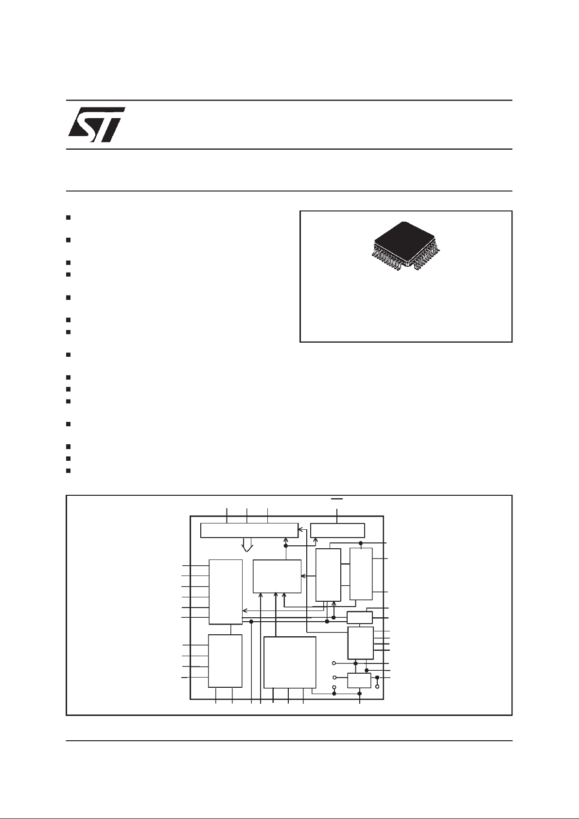
BLOCKDIAGRAM
ORDERING NUMBERS: STLC3055Q
DESCRIPTION
The STLC3055 is a SLIC device specifically designed for WLL (Wireless Local Loop) and ISDNTerminalAdaptors. One of the distinctive characteristic of this device is theability to operate with
a single supply voltage (from +5.5V to +15.8V)
and self generate the negative battery by means
of an on chip DC/DC converter controller that
drives an externalMOSswitch.
The battery level is properly adjusted depending
on the operatingmode. A useful characteristic for
TQFP44
STLC3055QTR
October 1999
TX
RX
ZAC1
ZAC
RS
ZB
CKTTX
CTTX1
CTTX2
FTTX
D0 D1 D2 DET
INPUT LOGICAND DECODER
Status and functions
SUPERVISION
AC PROC
TTX PROC
RTTX CAC ILTF RD IREF RLIM RTH
REFERENCE
OUTPUT LOGIC
LINE
DRIVER
Vcc
Vss
Agnd
OUTPUT
STAGE
DC PROC
DC/DC
CONV.
VOLT.
REG.
AGND
Vbat
BGND
TIP
RING
CREV
CSVR
CLK
RSENSE
GATE
VF
CVCC
VPOS
VBAT
1/22
Page 2
STLC3055
DESCRIPTION (continued)
these applications is the integratedringing generator.
The control interface is a parallel type with open
drainoutput and3.3V logiclevels.
The metering pulses are generated on chip starting fromtwo logic signals(0, 3.3V) one define the
metering pulse frequency and the other the meteringpulse duration. An on chipcircuit then provides the proper shaping and filtering. Metering
pulse amplitude and shaping (rising and decay
time) can be programmed by external components. A dedicated cancellation circuit avoid pos-
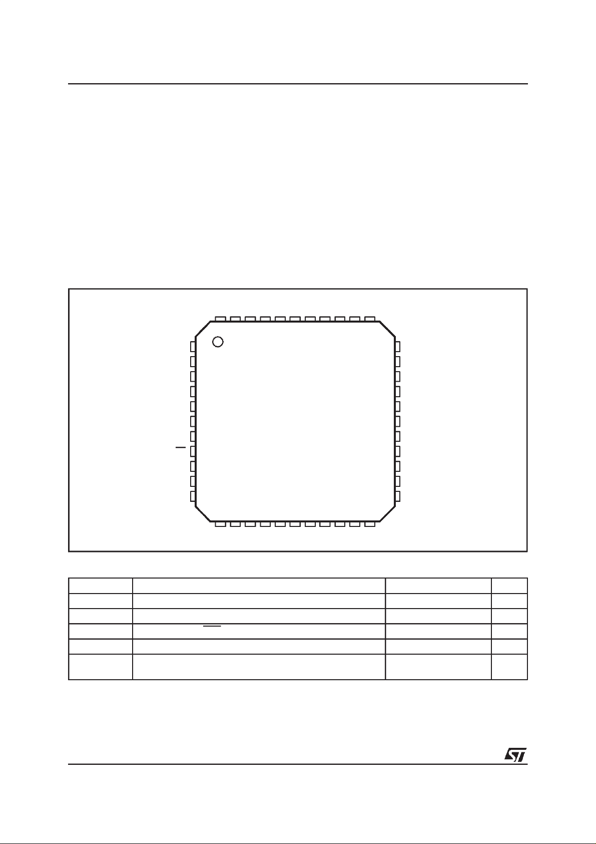
PIN CONNECTION
VBAT1
CREV
N.C.
TIP
44 43 42 41 3940 38 37 36 35 34
sible CODEC input saturation due to Metering
pulse echo.
Constant current feed can be set from 20mA to
40mA. Off-hook detection threshold is programmable from 5mAto 9mA.
The device, developed in BCD100II technology
(100V process), operates in the extended temperature range and integrates a thermal protection that sets the device in power down when Tj
exceeds140°C.
N.C.
N.C.
N.C.
RING
N.C.
VBAT
BGND
RES
N.C.
N.C.
DET
CKTTX
CTTX1
CTTX2
1
D0
2
D1
3
D2
4
PD
5
6
7
8
9
10
12 13 14 15 16
RX
FTTX
RTTX
171118 19 20 21 22
ZB
RS
ZAC
ZAC1
CAC
TX
VF
CLK
33
32
31
30
29
28
27
26
25
24
23
D97TL279A
CSVR
ILTF
RD
RTH
IREF
RLIM
AGND
CVCC
VPOS
RSENSE
GATE
ABSOLUTEMAXIMUM RATINGS
Symbol Parameter Value Unit
V
pos
A/BGND AGND to BGND -1 to +1 V
V
dig
T
j
(1)
V
btot
Positive Supply Voltage -0.4 to +17 V
Pin D0, D1, D2, DET, CKTTX -0.4 to 5.5 V
Max. junction Temperature 150 °C
Vbtot=|Vpos|+|Vbat|. (Totalvoltage applied tothe device
100 V
supply pins).
(1) Vbat is selfgenerated bythe on chip DC/DC converter and can be programmed via RF1 and RF2.
RF1and RF2 shall beselected in order tofulfil the a.mlimits (see External Components Table page 10)
2/22
Page 3
STLC3055
OPERATINGRANGE
Symbol Parameter Value Unit
V
pos
A/BGND AGND to BGND -100 to +100 V
V
dig
T
op
(1)
V
bat
(1) Vbat is selfgenerated bythe on chip DC/DC converter and can be programmed via RF1 and RF2.
RF1and RF2 shall beselected in order tofulfil the a.mlimits (see External Components Table page 10)
THERMALDATA
Symbol Parameter Value Unit
R
thj-amb
PIN DESCRIPTION
N. Name Function
25 VPOS Positive supply inputranging from 5.5Vto 15.8V.
34 BGND Battery Ground, must beshorted with AGND.
27 AGND Analog Ground, must be shortedwith BGND.
16 ZAC AC impedance synthesis.
15 ZAC1 RX bufferoutput, the AC impedanceis connected fromthis node to ZAC.
17 RS Protection resistors image (theimage resistor is connectedfrom this node to ZAC).
18 ZB Balance Networkfor 2 to 4 wire conversion (the balanceimpedance ZB is connectedfrom this
20 TX 4 wire output port (TXoutput). The signal is referred toAGND. If connected to single supply
14 RX 4 wireinput port (RX input); 300KΩinput impedance. This signal is referred to AGND. If
19 CAC AC feedbackinput, AC/DC split capacitor (CAC).
32 ILTF Transversal line current image output.
41 TIP 2 wire port; TIP wire (Ia is the current sourced from this pin).
37 RING 2 wire port;RING wire (Ib is the current sunk into thispin).
28 RLIM Constant current feedprogramming pin (viaRLIM). RLIM should be connected close to this
30 RTH Off-hook threshold programming pin (via RTH).RTH should be connected close to this pin
29 IREF Internal bias current setting pin. RREF should be connected close to this pin and PCB layout
43 CREV Reverse polaritytransition time control.One proper capacitor connected between thispin and
31 RD DC feedback and ring trip input. RD should be connected closeto this pin and PCBlayout
Positive Supply Voltage 5.5 to +15.8 V
Pin D0, D1, D2, DET, CKTTX, PD -0.25 to 5.25 V
Ambient Operating Temperature Range -40 to +85 °C
Self Generated Battery Voltage -74 max. V
Thermal Resistance Junctionto Ambient Typ. 60 °C/W
node to AGND. ZA impedance is connected from this node to ZAC1).
CODEC input it must beDC decoupled with proper capacitor.
connected to single supply CODECoutput itmust beDC decoupledwith proper capacitor.
pin andPCB layout should avoid noise injection on this pin.
and PCB layout should avoid noise injectionon this pin.
should avoid noise injection on this pin.
AGND is setting the reverse polarity transitiontime. This is the same transitiontime used to
shape the”trapezoidal ringing” during ringing injection.
should avoid noise injection on this pin.
3/22
Page 4
STLC3055
PIN DESCRIPTION (continued)
N. Name Function
4 PD Power Down input. Normally connected to CVCC (or to logic level high). Can beused to set
26 CVCC Internal positive voltage supplyfilter.
35 VBAT Regulated battery voltage self generated by the device via DC/DC converter. Must be shorted
23 GATE Driver for external Power MOS transistor.
21 VF Feedback inputfor DC/DC converter controller.
22 CLK Power Switch ControllerClock (typ. 125KHz). From version marked STLC3055 A5, this pin
24 RSENSE Voltage input for current sensing. RSENSE should beconnected close to this pin and VPOS
1 D0 Control Interface: input bit0.
2 D1 Control Interface: input bit1.
3 D2 Control interface: input bit 2.
8 DET Logic interface output of the supervision detector(active low).
33 CSVR Battery supply filter capacitor.
12 RTTX Metering pulse cancellation buffer output. TTX filter network should be connected to this point.
13 FTTX Metering pulse buffer input this signal is sent to the line andused to perform TTX filtering.
10 CTTX1 Metering burst shaping external capacitor.
11 CTTX2 Metering burst shaping external capacitor.
9 CKTTX Metering pulse clock input (12 KHz or 16KHz square wave).
44 VBAT1 Frame connection. Must be shorted to VBAT.
5 RES Reserved, must be connected toAGND.
6, 7,36,
38,39,
40,42
NC Not connected.
FUNCTIONALDESCRIPTION
The STLC3055 is a device specifically developed
for WLL and ISDN-TAapplications.
It is based on a SLIC core, on purpose optimised
for these applications, with the addition of a
DC/DC converter controller to fulfil the WLL and
ISDN-TAdesignrequirements.
The SLIC performs the standard feeding, signallingand transmissionfunctions.
It can be set in three different operating modes
via the D0, D1, D2 pins of the control logic interface (0 to 3.3V logic levels). The loop status is
carriedout onthe DET pin (activelow).
The DETpin is an opendrain output to alloweasy
interfacingwithboth 3.3Vand 5Vlogic levels.
The fourpossible SLIC’soperatingmodes are:
Power Down
TIP andRing terminals in open circuitsetting PD=0 and D0=D1=0.
to VBAT1.
can also be connected to CVCC or AGND. Whenthe CLK pin is connected toCVCC an
internal auto-oscillation is internally generatedand it is used instead of the external clock.
When the CLK pin is connected to AGND, theGATE output is disabled.
pin. The PCB layoutshould minimize the extra resistanceintroduced bythe copper tracks.
If notused should be left open.
HighImpedanceFeeding (HI-Z)
Active
Ringing
Table 1shows how to set the differentSLIC operatingmodes.
Table1. SLICoperatingmodes.
PD D0 D1 D2 Operating Mode
0 0 0 X Power Down
1 0 0 X H.I. Feeding(HI-Z)
1 0 1 0 Active NormalPolarity
1 0 1 1 Active ReversePolarity
1 1 1 0 Active TTX injection (N.P.)
1 1 1 1 Active TTX injection (R.P.)
1 1 0 0/1 Ring (D2 bit toggles @ fring)
4/22
Page 5

STLC3055
The DC/DC converter controller is driving an external power MOS transistor (P-Channel) in order
to generate the negative battery voltage needed
for device operation.
The DC/DC converter controller is synchronised
withan externalCLK (125KHZtyp.).
From version marked STLC3055 A5, it can be
synchronisedto an internalclock generatedwhen
the pin CLK is connected to CVCC. One sensing
resistor in series to Vpos supply allows to fix the
maximumallowed input peakcurrent.This feature
is implemented in order to avoid overload on
Vpos supply in case of line transient (ex. ring trip
detection).
The typical value is obtained for a sensing resistor equal to 110mΩ that will guarantee an average current consumptionfrom Vpos < 700mA.
When in on-hook the self generated battery voltage is set to a predefinedvalue.
This value can be adjustedvia one externalresistor (RF1) and it is typical -50V. When RINGmode
is selectedthis valueis increasedto -70V typ.
Once the line goes in off-hook condition, the
DC/DC converter automatically adjust the generated battery voltage in order to feed the line with
a fixedDC current(programmablevia RLIM) optimising in this way the power dissipation.
This operating mode is normally selected when
the telephoneis in on-hook in order to monitorthe
line status keeping the power consumption at the
minimum.
The output voltage in on-hook condition is equal
totheself generatedbatteryvoltage(-50V typ).
When off-hook occurs the DET becomes active
(lowlogic level).
The off-hook threshold in HI-Z mode is the same
value asprogrammed inACTIVE mode.
The DC characteristic in HI-Z mode is just equal
to the self generated battery with 2x(1500W+Rp)
in series (see fig.1), where Rp is the externalprotectionresistance.
Figure1. DCCharacteristicin HI-Z Mode.
IL
Vbat
2x(R1+Rp)
Slope: 2x(R1+Rp)
(R1=1500ohm)
OPERATINGMODES
Power Down
DC CHARACTERISTIC& SUPERVISION
Whenthis modeis selected theSLIC is switched
off and the TIP and RING pins are in high impedance. Also the line detectorsare disabled thereforethe off-hookconditioncannot be detected.
This mode can be selected in emergency condition when it is necessary to cut any current deliveredto the line.
This mode is alsoforced by STLC3055 in case of
thermaloverload(Tj > 140°C).
In this case the device goes back to the previous
status as soon as the junction temperature decreaseunder the hysteresisthreshold.
AC CHARACTERISTICS
The 2W port is set in high impedance, the TX
output buffer is a low impedance output, no AC
transmissionis possible.
High Impedance Feeding (HI-Z)
DC CHARACTERISTIC& SUPERVISION
VL
Vbat (-50V)
AC CHARACTERISTICS
The AC impedance shown at the 2W port
(TIP/RING) is the same as the DC one. The
TIP/RINGAC impedance will be 2x(1500Ω+ Rp)
or highimpedance.
Active
DC CHARACTERISTICS & SUPERVISION
When this mode is selected the STLC3055 pro-
videsboth DC feedingandAC transmission.
The STLC3055 feedsthe line witha constantcur-
rent fixed by RLIM (20mA to 40mA range). The
on-hook voltage is typically 40V allowing on-hook
transmission;the selfgeneratedVbat is-50V typ.
If the loop resistance is very high and the line
current cannot reach the programmed constant
currentfeed value,the STLC3055 behaveslike a
40V voltage source with a series impedance
equal to the protection resistors 2xRp (typ.
2x41Ω) plus the internal resistance. Fig. 2 shows
thetypical DCcharacteristicin ACTIVE mode.
5/22
Page 6

STLC3055
Figure2. DC characteristicin ACTIVE mode
IL
Ilim
(20 to
40mA)
2Rp
10V
VL
Vbat (-50V)
The line status (on/off hook) is monitored by the
SLIC’s supervision circuit. The off-hook threshold
can be programmed via the externalresistor R
TH
in the range from5mA to 9mA.
Independentlyon the programmed constant cur-
rent value, the TIP and RING buffers have a currentsource capabilitylimited to70mA typ.
Moreover the power available at Vbat is controlled by the DC/DC converter that limits the peak
current drawn from the Vpos supply. The maximum allowed current peak is set by the R
SENSE
resistorand it is typically900mApk.
POLARITYREVERSAL
The D2 bit controls the line polarity, the transition
betweenthe two polaritiesis performed in a ”soft”
way. This means that the TIP and RING wire exchange their polarities following a ramp transition
(see fig.3). The transition time is controlled by an
external capacitor CREV. This capacitor is also
setting the shape of the ringing trapezoidal waveform.
Whenthe control pins set battery reversal the line
polarity is reversed with a proper transition time
setvia an externalcapacitor(CREV).
Figure3. TIP/RING typical transitionfrom
Directto ReversePolarity
GND
TIP
4V typ.
40V typ
ON-HOOK
dV/dT set
by CREV
RING
AC CHARACTERISTICS
The SLIC provides the standard SLIC transmis-
sion functions:
Input impedance synthesis: can be real or
complex and is set by a scaled (x50) external
ZACimpedance.
Transmit and receive: The AC signal present
on the 2W port (TIP/RING)is transferredto the
TX outputwith a -6dBgain and from the RX input to the2W portwith a 0dBgain.
2 to 4 wire conversion: The balance impedance can be real or complex, the proper cancellation is obtained by means of two external
impedanceZA and ZB.
Once in Active mode (D1=1) the SLIC can operate in different states setting properly D0 and D2
controlbits (see also Table 2).
Table2. SLICstates in ACTIVEmode
D0 D1 D2 Operating Mode
0 1 0 Active Normal Polarity
0 1 1 Active Reverse Polarity
1 1 0 Active TTX injection (N.P.)
1 1 1 Active TTX injection (R.P.)
METERING PULSE INJECTION(TTX)
The metering pulses circuit consist of a burst
shaping generator that gives a square wave
shaped and a low pass filter to reduce the harmonic distortionof theoutput signal.
The metering pulse is obtained starting from two
logicsignals:
CKTTX: is a square wave at the TTX frequency (12 or 16KHz) and should be permanently applied to the CKTTX pin or at least for
all the duration of the TTX pulse (including rising and decayphases).
D0: enable the TTX generation circuit and definethe TTXpulse duration.
This two signals are then processed by a dedicated circuitry integrated on chip that generate
the metering pulse as an amplitude modulated
shaped squarewave (SQTTX)(see fig.4).
Both the amplitude and the envelope of the
squarewave (SQTTX) can be programmed by
means of external components. In particular the
amplitudeis set by the two resistorsRLV and the
6/22
Page 7
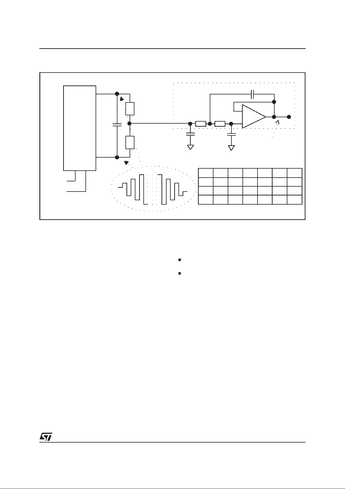
Figure4. Meteringpulse generationcircuit.
CTTX1
STLC3055
Low PassFilter
C1
RLV
BURST
SHAPING
GENERATOR
D0
CKTTX
Square wavepulse metering
CS
CTTX2
SQTTX
RLV
shapingby thecapacitorCS.
The waveform so generated is then filtered and
injectedon the line.
The lowpass filtercan be obtained usingthe inte-
grated buffer OP1 connected between pin FTTX
(OP1 non inverting input) and RTTX(OP1 output)
(see fig.4) and implementing a ”Sallen and Key”
configuration.
Dependingon the externalcomponents count it is
possible to build an optimised application depending on the distortion level required. In particular harmonic distortion levels equal to 13%,
6% and 3% can be obtained respectively with
first,second andthirdorder filters(see fig.4).
The circuit showed in the ”Applicationdiagram” is
relatedto thesimple firstorderfilter.
Once the shaped and filtered signal is obtained at
RTTX buffer outputit is injectedon the TIP/RING
pins with a +6dBgain.
It should be noted that this is the nominal condition obtained in presence of ideal TTX echo cancellation(obtained via proper settingof RTTXand
CTTX). In addition the effective level obtained on
the line will depend on the line impedance, the
protection resistor value and the series switch
(SW1or SW2)on resistance.
In the typical application (TTX line impedance
=200Ω ,RP=41Ω, SW1,2 on resistance = 9Ω
and ideal TTX echo cancellation) the metering
pulse level on the line will be 1.33 timesthe level
appliedto theRTTX pin.
RTTX
R1
CFL
R2
FTTX
OP1
+
C2
Sinusoidalwave
pulse metering
Required external components vs.filter order.
Order CFL R1 C! R2 C2 THD
1 X 13%
2 XXXX6%
3XXXXX3%
As already mentioned the metering pulse echo
cancellationis obtained by means of two external
components(RTTXand CTTX) thatshould match
the line impedance at the TTX frequency. This
simplenetwork has a doubleeffect:
Synthesise a low output impedance at the
TIP/RINGpins at theTTXfrequency.
Cut the eventual TTX echo that will be transferredfromthe line tothe TX output.
Ringing
When this mode is selected STLC3055 self generate an higher negativebattery (-70V typ.) in order to allow a balanced ringing signal of typically
65Vpeak.
In this condition both the DC and AC feedback
loop are disabled and the SLIC line drivers operateas voltagebuffers.
The ring waveform is obtained toggling the D2
controlbit atthedesired ringfrequency.This bitin
fact controls the line polarity (0=direct; 1=reverse). As in the ACTIVE mode the line voltage
transition is performed with a ramp transition,obtaining in this way a trapezoidal balanced ring
waveform(seefig.5).
The shaping is defined by the CREV external
capacitor.
Selecting the proper capacitor value it is possible
toget differentcrest factorvalues.
The following table shows the crest factor values
7/22
Page 8

STLC3055
Figure 5. TIP/RING typical ringingwaveform
GND
2.5V typ.
TIP
65V
typ.
dV/dT set
byCREV
RING
VBAT
2.5V typ.
obtained with a 20Hz and 25Hz ring frequency
and with 1REN. This value are valid either with
Europeanor USA specification:
CREV
22nF 1.2 1.26
27nF 1.25 1.32
33nF 1.33 Not significant (*)
(*) Distorsion already less than 10%.
CREST
FACTOR
@20Hz
CREST
FACTOR
@25Hz
If for any reason the ringer load will be too high
the self generated battery will drop in order to
keep thepower consumptionto thefixed limit and
therefore also the ring voltage level will be reduced.
In the typical application with R
SENSE
= 110mΩ
the peak current from Vpos is limited to about
900mA, which correspond to an average current
of 700mA max. In this condition the STLC3055
can drive up to 3REN with a ring frequency
fr=25Hz (1REN = 1800Ω + 1.0µF, European
standard).
In order to drive up to 5REN (1REN= 6930Ω +
8µF, US standard) it is necessary to modify the
externalcomponentsas follows:
CREV = 15nF
RD = 2.2KΩ
Power On Requirements
In order to avoid damage to the device when
Vpos is first appliedit is recommendedto keep all
the logic inputs to a lowlogic level (0V)until Vpos
is >5.5V.
In case this power up sequence cannot be guaranteed it’s recommended to connect a shottkydiode (BAT46 or equivalent) between VBAT and
BGNDsee figurebelow.
The ring trip detection is performed sensing the
variation of the AC line impedance from on hook
(relatively high) to off-hook (low). This particular
ring tripmethod allows to operatewithoutDC offset superimposed on the ring signal and therefore
obtaining the maximumpossible ring level on the
load starting from a givennegative battery.
It should be noted that such a method is optimised for operationon shortloop applicationsand
may not operateproperly in presenceof long loop
applications(>500Ω ).
Once ring trip is detected,the DET output is activated (logic level low), at this point the card controller or a simple logic circuitshould stop the D2
toggling in order to effectivelydisconnect the ring
signal and then set the STLC3055 in the proper
operatingmode (normallyACTIVE).
RING LEVEL IN PRESENCE OF MORE TELEPHONEIN PARALLEL
As already mentioned above the maximum current that can be drawn from the Vpos supply is
controlledand limitedvia theexternal RSENSE.
This will limit also the power available at the self
generatednegative battery.
Figure 6. Shottkydiode connection
BGND
STLC3055
VBAT
BAT46
8/22
Page 9

STLC3055
LayoutRecommendation
A properly designed PCB layout is a basic issue
to guarantee a correct behaviour and good noise
performances.
Particularcare must be taken on the ground connection and in this case the star configuration allowssurely to avoid possibleproblems(see ApplicationDiagram Fig. 7).
The ground of the power supply (VPOS) has to
be connected to the center of the star, let’s call
this point PGND. This point shouldshow a resistance as low as possible, that means it should be
a groundplane.
Noise sources can be identified in not enough
good grounds, not enough low impedance supplies and parasitic coupling between PCB tracks
and high impedancepins of the device.
In particular to avoid noise problems the layout
should prevent any coupling between the DC/DC
converter components and analog pins that are
referred to AGND (ex: RD, IREF, RTH, RLIM,
VF). As a first reccomendation the components
CV, L, D1, CVPOS, RSENSE should be kept as
close as possible to each other and isolated from
the other components.
Additionalimprovements can be obtained:
decoupling the center of the star from the analog ground of STLC3055using smallchokes.
adding a capacitor in the range of 100nF between VPOS and AGND in order to filter the
switchfrequency on VPOS.
ExternalComponents List
In order to properly define the external components value the following system parameters
have to be defined:
The ACinput impedanceshown by the SLIC at
the line terminals ”Zs” to which the return loss
measurement is referred. It can be real (typ.
600Ω) or complex.
The AC balance impedance, it is the equivalent impedance of the line ”Zl” used for evaluation of the trans-hybrid loss performances
(2/4 wire conversion). It is usually a complex
impedance.
The value of the two protection resistors Rp in
series with theline termination.
The line impedance at the TTX frequency
”Zlttx”.
The metering pulse level amplitude measured
at line termination ”V
der filtering, V
LOTTX
”. In case of low or-
LOTTX
represents the amplitude
(Vrms) of the fundamental frequency component.(typ 12 or 16KHz).
Pulse metering envelope rise and decay time
constant”τ”.
The slope of the ringing waveform”∆V
TR
/
”.
∆
T
The value of the constant current limit current
”Ilim”.
The value of the off-hook current threshold
”.
”I
TH
The value of the ring trip rectified average
thresholdcurrent”I
RTH
”.
The value ofthe requiredself generated negative battery ”V
” in ring mode (max value
BATR
is 70V). This value can be obtained from the
desiredring peak level +5V.
The value of the maximum current peak sunk
fromVpos ”IPK”.
9/22
Page 10

STLC3055
EXTERNAL COMPONENTS
Name Function Formula Typ. Value
RREF Bias setting current RREF = 1.3/Ibias
Ibias = 50µA
CSVR Negative Battery Filter CSVR = 1/(2π ⋅ fp ⋅ 1.8MΩ)
fp = 50Hz
RD Ring Trip threshold setting
resistor
RD = 100/I
RTH
2KΩ<RD<5K
Ω
CAC AC/DC split capacitance 22µF 20% 15VL
RP Line protection resistor Rp > 30Ω 41Ω 1%
RS Protection and series switches
RS = 100 ⋅ (Rp + 9Ω)5kΩ@Rp=41Ω
resistance image
ZAC Two wire AC impedance ZAC = 50⋅(Zs - 2Rp -18Ω) 25kΩ1%
ZA (1) SLIC impedancebalancing
ZA = 50 ⋅ Zs 30kΩ 1%
network
ZB (1) Line impedance balancing
ZB = 50⋅Zl 30kΩ1%
network
CCOMP AC feedback loop compensation CCOMP = 1/(2π⋅fo⋅100⋅(RP+9Ω))
fo = 250kHz
CH Trans-Hybrid Loss frequency
CH = CCOMP 120pF 10% 10VL
compensation
RLIM Current limiting programming RLIM = 1300/Ilim
RTH Off-hook threshold programming
(ACTIVE mode)
CREV Reverse polarity transition time
32.5kΩ< RLIM < 65k
RTH = 260/I
TH
27kΩ <RTH < 52kΩ
CREV = (1/3750) ⋅ ∆T/∆V
Ω
) 22nF 10% 10V
TR
programming
RTTX (3) Pulse metering cancellation
RTTX = 50Re[(Zlttx+2Rp+18Ω)] 15k
resistor
CTTX (3) Pulse metering cancellation
CTTX = 1/{50⋅2π⋅fttx[-lm(Zlttx)]} 100nF 10% 10V (2)
capacitor
RLV Pulse metering level resistor RLV = 63.3⋅10
= (|Zlttx + 2Rp + 18Ω|/|Zlttx|)
α
CS Pulse metering shaping
CS =τ/(2⋅RLV) 100nF 10% 10V
capacitor
3
⋅α⋅V
LOTTX
@τ= 6ms, RLV = 27.1k
CFL Pulse metering filter capacitor CFL = 2/(2π⋅fttx⋅RLV) 1nF 10% 10V
RDD Pull up resistors 100k
CVCC Internally supply filter capacitor 100nF 20% 10V
CVpos Positive supply filter capacitor
with low impedance for switch
mode power supply
CV Battery supply filter capacitor
with low impedance for switch
mode power supply
CVB High frequencynoise filter 470nF 20% 100VL
26kΩ1%
1.5nF 10%
100VL
4.12kΩ1%
@ IRTH =24mA
@ RD = 4.12kΩ
@ Zs= 600
@ Zs= 600Ω
@ Zl = 600
120pF 10% 10VL
@Rp=41
52.3kΩ1%
@ Ilim = 25mA
28.7kΩ1%
@ITH= 9mA
@ 12V/ms
@Zlttx = 200Ωreal
@ Zlttx = 200Ω real
27kΩ 1%
@V
LOTTX
@fttx = 12kHz
RLV = 27k
100µF(4)
100µF 20% 100V(5)
Ω
Ω
Ω
Ω
= 275mVrms
Ω
Ω
Ω
10/22
Page 11

EXTERNAL COMPONENTS(continued)
Name Function Formula Typ. Value
CRD (6) High frequency noise filter 100nF 10% 15VL
Q1 DC/DC converter switch P ch.
MOS transistor
RDS(ON)≤1.2Ω,VDS = -100V
Total gate charge=20nC max.
with VGS=4.5Vand VDS=1V
ID>500mA
D1 DC/DC converter series diode Vr > 100V, t
RSENSE DC/DC converter peak current
RSENSE = 100mV/I
50ns SMBYW01-200
≤
RR
PK
limiting
L (8) DC/DC converterinductor DC Resistance≤0.1Ω(9) L=125µH RFP1304PV
CF1 DC/DC converter feedback loop
stability
RF1 Negative battery programming
250KΩ<RF1<300KΩ(7) 300kW 1%
level
RF2 Negative battery programming
level
Possible choiches:
IRF9510 or IRF9520or
IRF9120 or equivalent
or equivalent
110mΩ
@I
= 900mA
PK
(Manuf.: All Inductive)
or SUMIDA CDRH125
or equivalent
220pF to470pF (10)
@V
BATR
9.1kΩ 1%
STLC3055
= -70V
(1) In caseZs=Zl, ZA and ZB can bereplaced by two resistors of same value:RA=RB=|Zs|.
(2) In thiscase CTTXis justoperating as a DC decouplingcapacitor (fp=100Hz).
(3) Defining ZTTXas theimpedance ofRTTX in series with CTTX,RTTX and CTTXcanalso be calculated from the following formula:
ZTTX=50*(Zlttx+2Rp+18Ω).
(4) CVpos should be defined depending on the power supply currentcapability and maximum allowable ripple.
(5) For lowripple application use 2x47µF in parallel.
(6) Can be saved if proper PCB layout avoid noise coupling on RD pin (high impedanceinput).
(7) RF1 setsthe selfgenerated battery voltage in RING and ACTIVE(Il=0) mode asfollows:
267k
Ω
V
BAT(ACTIVE)
V
BATR(RING)
VBATR should be defined considering the ringpeak level required (Vringpeak=VBATR-6V typ.).
The above relation is valid provided that the Vpos power supply current capability and the RSENSE programming allow to source all the
current requested by the particularringer loadconfiguration.
(8) Core: MICROMETALS T50-26CIRON POWDER, AL-VALUE 61nH/N2
Current rating: 2A (50/60Hz)
Operating Temperature -25° to+60° Centigrades
Inductance: 14µH +/-15% at1KHz, 1mA
DC resistance of winding:MAX.100 mOhm
Code: RFY1303
Wire: UEW2,0,60 mm
Turns: 50
Inductance (f=1KHz): >125µH
(9) For highefficiency in HI-Z mode coil resistance @125kHz must be <3ohm
(10) Functionof thiscapacitor is to introduce a zero at the resonance frequency for loopstability.In case some parasitic resistance are already
present in the loop (Coil, CVBAT, PCB layout), the presence of this capacitor can degrade the device noise performances; in this case CF1
should be removedbeing the loop stabilityalready guaranteed by theparasitic resistance.
-46V -48V -49V -50V
-62V -65V -68V -70V
280k
Ω
294kW 300k
Ω
11/22
Page 12

STLC3055
Figure6. ApplicationDiagram.
CCOMP
CONTROL
INTERFACE
SUGGESTED GROUND LAY-OUT
TTX CLOCK
D0
D1
D2
SUPPLY GND
CFL
VDD
CH
RDD
RLV
RLV
ZAC
RD
CVPOS
RD
VPOS
RSENSE
GATE
VBAT
CLK
RING
CSVR
CREV
RTH
RLIM
IREF
CRD
RSENSE
TIP
CLK
RREF
CVB
RP
RP
CREV
RLIM
CF1
D96TL275D
TIP
RING
RF1
RF2
RTH
CSVR
Q1
D1
L
CVVF
RX
TX
TX
AGND VPOS
RS
RX
RS
ZAC
ZAC1
ZA
ZB
ZB
DETDET
D0
D1
D2
CKTTX
CTTX1
CS
CTTX2
FTTX
RTTX
RTTX
AGND
BGND
PGND
CTTX
CVCC
BGND CVCC
STLC3055
CAC
ILTF
CAC
Figure7. ApplicationDiagramwithout MeteringPulse Generation.
RD
CVPOS
RD
VPOS
RSENSE
GATE
VBAT
CLK
RING
CSVR
CREV
RTH
RLIM
IREF
CRD
RSENSE
TIP
CCOMP
CONTROL
INTERFACE
SUGGESTED GROUND LAY-OUT
TTX CLOCK
D0
D1
D2
SUPPLY GND
VDD
CH
RDD
ZAC
RX
TX
TX
AGND VPOS
RS
RX
RS
ZAC
ZAC1
ZA
ZB
ZB
CVCC
BGND CVCC
STLC3055
DETDET
D0
D1
D2
CKTTX
CTTX1
CTTX2
FTTX
AGND
BGND
PGND
RTTX
CAC
ILTF
CAC
CLK
RREF
CVB
RP
RP
CREV
RLIM
CF1
D98TL380A
TIP
RING
RF1
RF2
RTH
CSVR
Q1
D1
L
CVVF
12/22
Page 13

STLC3055
ELECTRICAL CHARACTERISTICS
Testconditions:V
Externalcomponentsas listedin the ”Typical Values” columnof EXTERNAL COMPONENTSTable.
Note: Testing of all parameteris performedat 25°C. Characterisation aswell as design rules used allow
correlationof tested performancesat other temperatures.All parameterslisted here are met in the operating range: -40to +85°C.
DC CHARACTERISTICS
Symbol Parameter Test Condition Min. Typ. Max. Unit
V
lohi
V
lohi
V
loa
V
loa
Ilim Lim. currentprogramming range ACTIVE mode 20 40 mA
Ilima Lim. current accuracy ACTIVE mode.
Rfeed HI Feeding resistance HI-Z (High Impedance feeding) 2.4 3.6 k
Zrx RX port input impedance 280 k
AC CHARACTERISTICS
L/T Long. totransv.
T/L Transv. to long.
T/L Transv. to long.
2WRL 2W return loss 300 to 3400Hz,
THL Trans-hybrid loss 300 to 3400Hz,
Ovl 2W overload level at line terminals on ref. imped.
TXoff TX output offset ACTIVE N. P., R
G24 Transmit gain abs. 0dBm @ 1020Hz,
G42 Receive gain abs. 0dBm @ 1020Hz,
G24f TX gain variation vs. freq. rel. 1020Hz; 0dBm,
Line voltage Il = 0,HI-Z
Line voltage Il = 0,HI-Z
Line voltage Il = 0,ACTIVE
Line voltage Il = 0,ACTIVE
(see Appendix for test circuit)
(see Appendix for test circuit)
(see Appendix for test circuit)
= 6.0V,AGND = BGND,NormalPolarity,T
pos
(High impedance feeding)
T
= 0 to 85°C
amb
(High impedance feeding)
T
= -40to 85°C
amb
T
= 0 to 85°C
amb
T
= -40to 85°C
amb
Rel. to programmed value
20mA to 40mA
Rp = 41Ω, 1% tol.,
ACTIVE N. P., R
f = 300 to 3400Hz
Rp = 41Ω, 1% tol.,
ACTIVE N. P., R
f = 300 to 3400Hz
Rp = 41Ω, 1% tol.,
ACTIVE N. P., R
f = 1kHz
ACTIVE N. P., R
20Log|VRX/VTX|,
ACTIVE N. P., R
ACTIVE N. P., R
ACTIVE N. P., R
ACTIVE N. P., R
300 to 3400Hz,
ACTIVE N. P., R
=25°C.
amb
44 50 V
42 48 V
33 40 V
31 37 V
-10 10 mA
48 50 dB
= 600Ω(*)
L
40 45 dB
= 600Ω(*)
L
48 53 dB
= 600Ω (*)
L
22 26 dB
= 600Ω(*)
L
30 dB
= 600Ω(*)
L
10 dBm
= 600Ω(*)
L
= 600Ω(*) -150 150 mV
L
-6.4 -5.6 dB
= 600Ω (*)
L
-0.4 0.4 dB
= 600Ω(*)
L
-0.12 0.12 dB
= 600Ω (*)
L
Ω
Ω
13/22
Page 14

STLC3055
ELECTRICAL CHARACTERISTICS(continued)
Symbol Parameter Test Condition Min. Typ. Max. Unit
G42f RX gain variation vs.freq. rel. 1020Hz; 0dBm,
300 to 3400Hz,
ACTIVE N. P., R
= 600Ω(*)
L
V2Wp Idle channelnoise at line psophometric filtered
ACTIVE N. P., R
T
= 0 to +85°C
amb
= 600Ω (*)
L
V2Wp Idle channelnoise at line psophometric filtered
ACTIVE N. P., R
T
= -40to +85°C
amb
= 600Ω(*)
L
V4Wp Idle channelnoise at line psophometric filtered
ACTIVE N. P., R
T
= 0 to +85°C
amb
= 600Ω(*)
L
V4Wp Idle channelnoise at line psophometric filtered
ACTIVE N. P., R
T
= -40to +85°C
amb
Thd Total Harmonic Distortion ACTIVE N. P., R
= 600Ω (*)
L
= 600Ω(*) -46 dB
L
VTTX Metering pulse level on line ACTIVE - TTX
Zl = 200Ωfttx = 12kHz
CLKfreq CLK operatingrange -10% 125 10% kHz
-0.12 0.12 dB
-73 -68 dBmp
-68 dBmp
-75 -70 dBmp
-75 dBmp
200 250 mVrms
(*) RL: Line Resistance
RING
Vring Line voltage RING D2 toggling@ fr = 25Hz
Load = 3REN;
Crest Factor =1.25
1REN = 1800Ω+ 1.0µF
T
= 0 to +85°C
amb
Vring Line voltage RING D2 toggling@ fr = 25Hz
Load = 3REN;
Crest Factor =1.25
1REN = 1800Ω + 1.0µF
T
= -40to +85°C
amb
DETECTORS
IOFFTHA Off/hook current threshold ACT. mode, RTH = 28.7kΩ1%
(Prog. ITH =9mA)
ROFTHA Off/hook loopresistance
threshold
ACT. mode, RTH = 28.7kΩ1%
(Prog. ITH =9mA)
IONTHA On/hook current threshold ACT. mode, RTH = 28.7kΩ 1%
(Prog. ITH =9mA)
RONTHA On/hook loopresistance
threshold
ACT. mode, RTH = 28.7kΩ1%
(Prog. ITH =9mA)
IOFFTHI Off/hook current threshold Hi Z mode, RTH =28.7kΩ1%
(Prog. ITH =9mA)
ROFFTHI Off/hook loop resistance
threshold
Hi Z mode, RTH = 28.7kΩ 1%
(Prog. ITH =9mA)
IONTHI On/hook current threshold Hi Z mode, RTH = 28.7kΩ1%
(Prog. ITH =9mA)
RONTHI On/hook loop resistance
threshold
Hi Z mode, RTH = 28.7kΩ1%
(Prog. ITH =9mA)
45 49 Vrms
44 48 Vrms
10.5 mA
3.4 k
Ω
6mA
8k
Ω
10.5 mA
800 Ω
6mA
8k
Ω
14/22
Page 15

STLC3055
ELECTRICAL CHARACTERISTICS(continued)
Symbol Parameter Test Condition Min. Typ. Max. Unit
Irt Ring Trip detectorthreshold
range
Irta Ring Trip detectorthreshold
accuracy
Trtd Ring trip detection time RING TBD ms
Td Dialling distortion ACTIVE -1 1 ms
Rlrt (1) Loop resistance 500 Ω
ThAl Tj for th. alarmactivation 160 °C
(1) Rlrt =Maximum loop resistance (incl.telephone) for correctring trip detection.
DIGITAL INTERFACE
INPUTS: D0, D1, D2, PD, CLK
OUTPUTS: DET
Vih In put highvoltage 2 V
Vil Input low voltage 0.8 V
Iih Input highcurrent -10 10
Iil Input low current -10 10
Vol Output low voltage Iol = 1mA 0.45 V
PSRR AND POWER CONSUMPTION
PSERRC Power supply rejection Vpos to
2W port
Ivpos Vpos supply current @ ii = 0 HI-Z On-Hook
Ipk Peak currentlimiting accuracy RING Off-Hook
RING 20 50 mA
RING -15 15 %
Vripple = 100mVrms
50 to 4000Hz
ACTIVE On-Hook,
RING (line open)
RSENSE = 110m
Ω
26 36 dB
52
93
120
-20% 950 +20% mApk
60
115
140
µ
µ
mA
mA
mA
A
A
15/22
Page 16

STLC3055
APPENDIX A
STLC3055Test Circuits
Referring to the application diagram shown in fig. 7 of the STLC3055 datasheet and using as external
components the Typ. Values specified in the ”External Components” Table (page 13) find below the
properconfigurationfor eachmeasurement.
All measurements requiring DC current termination should be performed using ”Wandel & Goltermann
DC Loop HoldingCircuit GH-1” or equivalent.
FigureA1. 2W Return Loss
2WRL= 20Log(|Zref+ Zs|/|Zref-Zs|) = 20Log(E/2Vs)
W&G GH1
Zref
TIP
600ohm
1Kohm
E
1Kohm
Vs
100µF
100mA
DC max
Zin = 100K
200 to 6kHz
100µF
STLC3055
application
circuit
TX
FigureA2. THLTrans HybridLoss
THL = 20Log|Vrx/Vtx|
W&GGH1
100µF
100mA
600ohm
DCmax
Zin= 100K
200 to 6kHz
100µF
TIP
STLC3055
application
RING
circuit
RING
RX
TX
Vtx
RX
Vrx
16/22
Page 17

FigureA3. G24TransmitGain
G24 = 20Log|2Vtx/E|
STLC3055
W&G GH1
600ohm
E
FigureA4. G42Receive Gain
G42 = 20Log|VI/Vrx|
Vl
600ohm
100µF
100mA
DC max
Zin = 100K
200to 6kHz
100µF
100µF
100mA
DC max
Zin = 100K
200 to 6kHz
100µF
W&G GH1
TIP
STLC3055
application
RING
TIP
RING
TX
Vtx
circuit
RX
TX
STLC3055
application
circuit
RX
FigureA5. PSRRCPowersupply rejection Vpos to 2Wport
PSSRC= 20Log|Vn/Vl|
W&G GH1
TIP
100µF
Vl
600ohm
100mA
DC max
Zin = 100K
200 to 6kHz
100µF
RING
STLC3055
application
circuit
VPOS
~
Vrx
TX
RX
Vn
17/22
Page 18

STLC3055
FigureA6. L/TLongitudinal toTransversal Conversion
L/T = 20Log|Vcm/Vl|
W&G GH1
100µF
100mA
DC max
Zin = 100K
200 to 6kHz
100µF
Vcm
300ohm
300ohm
100µF
Impedance matching
betterthan 0.1%
100µF
FigureA7. T/LTransversalto LongitudinalConversion
T/L = 20Log|Vrx/Vcm|
W&G GH1
100µF
100mA
DC max
Zin = 100K
200 to 6kHz
100µF
600ohm
Vcm
300ohm
100µF
Impedancematching
better than 0.1%
TIP
TX
STLC3055
Vl
application
circuit
RING
TIP
RX
TX
STLC3055
application
circuit
RING
RX
Vrx
300ohm
100µF
FigureA8. VTTXMeteringPulse level on line
Vlttx
200ohm
18/22
TIP
STLC3055
application
RING
circuit
CKTTX
TX
RX
fttx (12 or 16kHz)
Page 19

FigureA9. V2Wpand W4Wp: Idle channelpsophometric noise at line and TX.
V2Wp= 20Log|Vl/0.774l|;V4Wp = 20Log|Vtx/0.774l|
W&G GH1
STLC3055
TIP
100µF
STLC3055
application
circuit
RING
Vl
psophometric
filtered
600ohm
100mA
DC max
Zin = 100K
200 to 6kHz
100µF
APPENDIX B
STLC3055OvervoltageProtection
FigureB1. Simplifiedconfiguration for indoor overvoltage protection
BGND
2x
SM4T39RX
STLC3055
TIP
RING
RP1
RP1 RP2
RP2
TX
Vtx
psophometric
filtered
RX
TIP
RING
VBAT
RP2: Fuse orPTC
FigureB2. Standard overvoltage protection configurationfor K20compliance
BGND
2x
SM4T39RX
STLC3055
TIP
RING
VBAT
RP1 RP2
LCP1511
RP1 RP2
RP2:Fuse or PTC
TIP
RING
19/22
Page 20

STLC3055
APPENDIX C
TYPICALSTATEDIAGRAM FOR STLC3055OPERATION
FigureC1.
Tj>Tth
PD=0,D0=D1=0
Power
Down
Ring Burst
Normally used for
On Hook
Transmission
Active
On Hook
Ring Burst
Ring Pause
D0=0, D1=1,
D2=0
D0=1, D1=0, D2=0/1
PD=1, D0=D1=0
On HookDetection for T>Tref
HI-Z
Feeding
Active
On Hook Condition
Off Hook Detection
Off Hook
D0=0, D1=1,
D2=0
Note: all state transitionsare underthe microprocessor control.
Ringing
Ring Trip
Detection
Off HookDetection
20/22
Page 21

STLC3055
21/22
Page 22

STLC3055
Information furnished is believed to be accurate and reliable. However, STMicroelectronics assumes noresponsibility for the consequences
of use of such informationnor for any infringement of patents or other rights of third parties which may result from its use. No license is
granted by implication or otherwise under any patent or patent rights of STMicroelectronics. Specification mentioned in thispublication are
subject to change without notice. This publication supersedes and replaces all information previously supplied. STMicroelectronics products
are not authorized foruse as critical components in lifesupport devices or systems without express written approval of STMicroelectronics.
The ST logo is a registered trademark of STMicroelectronics
1999STMicroelectronics –Printed in Italy– AllRights Reserved
STMicroelectronics GROUP OF COMPANIES
Australia - Brazil- China - Finland - France- Germany- Hong Kong - India- Italy - Japan - Malaysia - Malta - Morocco -
Singapore- Spain - Sweden- Switzerland - United Kingdom -U.S.A.
http://www.st.com
22/22
 Loading...