

Page 1
STGW20NB60H
N-CHANNEL 20A - 600V TO-247
PowerMESH IGBT
TYPE V
CES
V
CE(sat)
I
C
ST G W20NB60H 600 V < 2 . 8 V 20 A
■ HIGHINPUT IMPEDANCE
(VOLTAGEDRIVEN)
■ LOW ON-VOLTAGEDROP (V
■ LOW GATECHARGE
■ HIGHCURRENTCAPABILITY
■ VERYHIGH FREQUENCYOPERATION
■ OFFLOSSES INCLUDETAIL CURRENT
CESAT
)
DESCRIPTION
Using the latest high voltage technology based
on a patented strip layout, STMicroelectronics
has designed an advanced family of IGBTs, the
PowerMESH IGBTs, with outstanding
perfomances. The suffix ”H” identifies a family
optimized to achieve very low switching times for
high frequencyapplications(<120kHz).
APPLICATIONS
■ HIGHFREQUENCY MOTOR CONTROLS
■ WELDINGEQUIPMENTS
■ SMPSAND PFC IN BOTH HARDSWITCH
AND RESONANTTOPOLOGIES
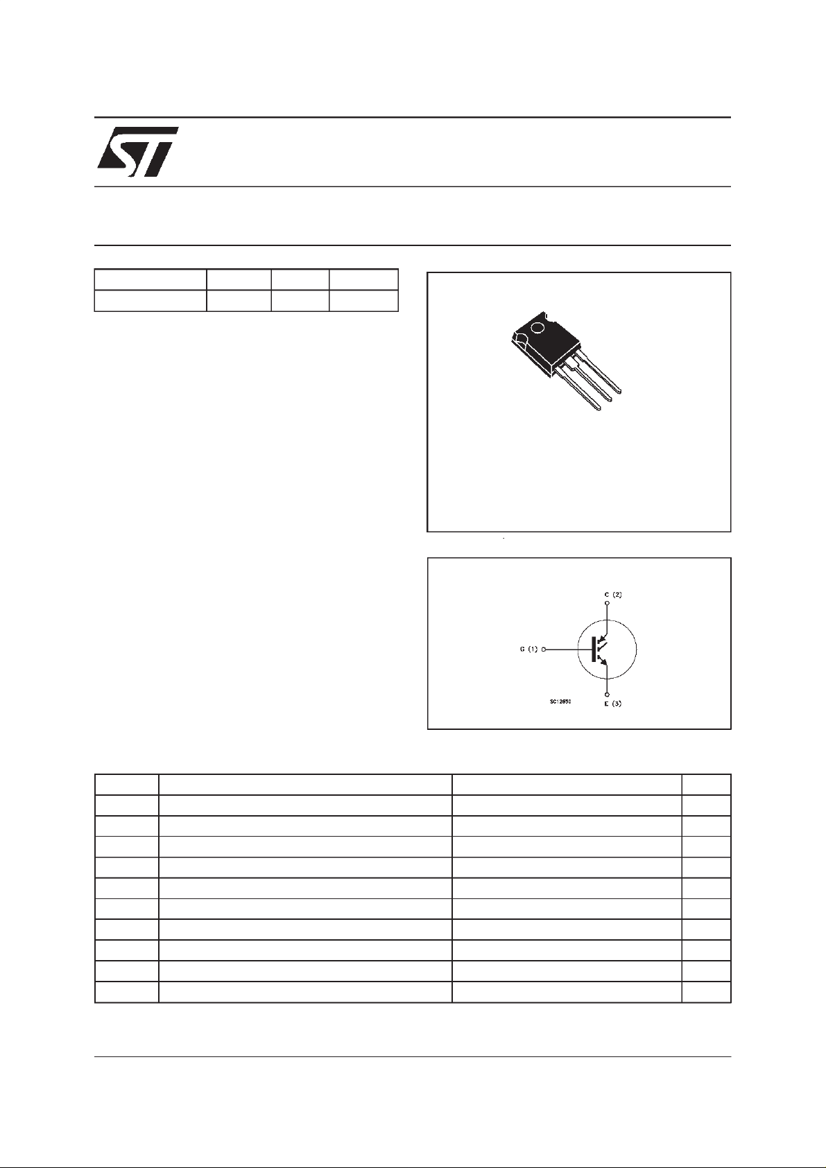
3
2
1
TO-247
INTERNAL SCHEMATIC DIAGRAM
ABSOLUTE MAXIMUM RATINGS
Symbol Parameter Value Unit
V
V
V
I
CM
P
T
(•) Pulsewidth limited by safeoperating area
June 1999
Collect o r -Em i t t er Voltage (VGS= 0) 600 V
CES
Emit t er-Collect or Voltage 20 V
ECR
Gate-Emitter V oltage
GE
I
Collect o r Curr ent (continuous) at Tc=25oC40A
C
I
Collect o r Curr ent (continuous) at Tc= 100oC20A
C
20 V
±
(•) Collect o r Curr ent (pulsed) 160 A
Tot al Dissipat ion at Tc=25oC 150 W
tot
Derat ing Factor 1.2 W/
Sto rage Tem perature - 65 to 150
stg
T
Max. Operat ing Junc tion Tem per ature 150
j
o
C
o
C
o
C
1/8
Page 2
STGW20NB60H
THERMAL DATA
R
thj-case
R
thj-amb
R
thc-h
Ther mal Resistanc e Junction-case Max
Ther mal Resistanc e Junction-ambient Max
Ther mal Resistanc e C as e - heatsink Typ
0.83
30
0.1
o
C/W
oC/W
o
C/W
ELECTRICAL CHARACTERISTICS
=25oC unless otherwise specified)
(T
j
OFF
Sym bol Param e t er Test Conditions Min . Typ. Max. Unit
V
BR(CES)
Collector-Emitter
IC=250µAVGE= 0 600 V
Break dow n Volt age
I
I
CES
GES
Collect o r cut - off
=0)
(V
GE
Gat e- Em i t t er Leakage
Current (V
CE
=0)
V
=MaxRating Tj=25oC
CE
=MaxRating Tj=125oC
V
CE
V
= ± 20 V VCE=0 ±100 nA
GE
10
100
ON(∗)
Sym bol Param e t er Test Conditions Min . Typ. Max. Unit
V
GE(th)
Gate Th reshold
VCE=VGEIC= 250 µ A35V
Voltage
V
CE(SAT)
Collector-Emitter
Sat urat ion Volt age
VGE=15V IC=20A
V
=15V IC=20A Tj= 125oC
GE
2.3
1.9
2.8 V
DYNAMIC
Sym bol Param e t er Test Conditions Min . Typ. Max. Unit
C
C
C
Q
Q
g
Q
I
CL
Forward
fs
Tr ansc on duc tance
Input Capacitanc e
ies
Out put Capacitance
oes
Reverse Transfer
res
Capacit a nc e
Tot al Gate Charge
G
Gate-Emitt er C harge
GE
Gat e- Col lect or C har ge
GC
Latc hing Curr ent V
VCE=25 V IC=20A 7.0 10 S
VCE=25V f=1MHz VGE= 0 1200
140
VCE= 480 V IC=20A VGE= 15 V 110
28
1700
200
40
2200
260
52
145 nC
13
51
=480V RG=10 Ω
clamp
T
= 150oC
j
80 A
µA
µ
V
pF
pF
pF
nC
nC
A
SWITCHINGON
Sym bol Param e t er Test Conditions Min . Typ. Max. Unit
(di/dt)
2/8
t
d(on)
E
Delay Time
t
Rise Time
r
Tur n-on Current Slope
on
Turn-on
on
Switching Losses
VCC= 480 V IC=20A
=15V RG=10Ω
V
GE
VCC=480V IC=20A
=10Ω VGE=15V
R
G
T
=125oC
j
20
70
350
300
ns
ns
A/µs
J
µ
Page 3
STGW20NB60H
ELECTRICAL CHARACTERISTICS
(continued)
SWITCHINGOFF
Sym bol Param e t er Test Conditions Min . Typ. Max. Unit
t
tr(v
t
d(off
E
off
E
t
tr(v
t
d(off
E
off
E
(•) Pulse width limited by max. junction temperature
(∗) Pulsed: Pulse duration = 300 µs, duty cycle 1.5%
(**)Losses Include Also The Tail (Jedec Standardization)
Cross-Over Time
c
Off Voltage Rise Time
)
off
)
Delay Time
t
Fall T ime
f
(**)
Turn-off Switching Loss
Tot al Switching Loss
ts
Cross-Over Time
c
)
Off Voltage Rise Time
off
)
Delay Time
t
Fall T ime
f
(**)
Turn-off Switching Loss
Tot al Switching Loss
ts
VCC=480V IC=20A
R
GE
=10
Ω
VGE=15V
VCC = 480 V IC=20A
R
GE
= 125oC
T
j
=10
Ω
VGE=15V
115
32
170
75
0.4
0.65
190
55
210
140
0.7
1.0
ns
ns
ns
ns
mJ
mJ
ns
ns
ns
ns
mJ
mJ
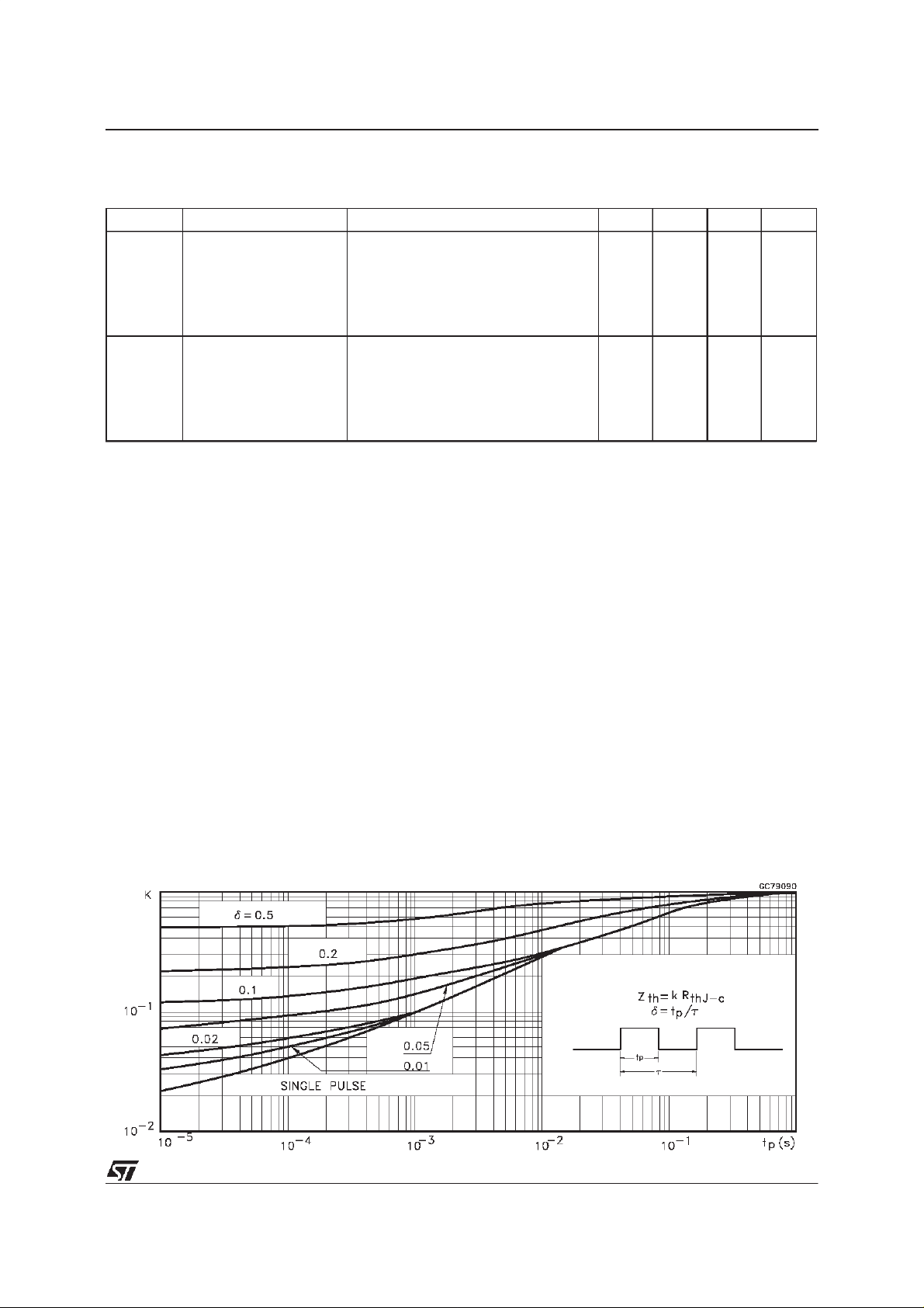
ThermalImpedance
3/8
Page 4

STGW20NB60H
OutputCharacteristics
Transconductance
TransferCharacteristics
Collector-EmitterOnVoltagevs Temperature
Collector-EmitterOnVoltagevs Collector Current
4/8
Gate Thresholdvs Temperature
Page 5

STGW20NB60H
NormalizedBreakdown Voltage vs Temperature
Gate Chargevs Gate-EmitterVoltage
CapacitanceVariations
TotalSwitchingLossesvs Gate Resistance
TotalSwitchingLossesvs Temperature
TotalSwitchingLossesvs Collector Current
5/8
Page 6

STGW20NB60H
SwitchingOff SafeOperatingArea
Fig. 1: GateChargetest Circuit
Fig. 3
: SwitchingWaveforms
Fig. 2: Test Circuit For InductiveLoad Switching
6/8
Page 7

TO-247 MECHANICAL DATA
STGW20NB60H
DIM.
MIN. TYP. MAX. MIN. TYP. MAX.
A 4.7 5.3 0.185 0.209
D 2.2 2.6 0.087 0.102
E 0.4 0.8 0.016 0.031
F 1 1.4 0.039 0.055
F3 2 2.4 0.079 0.094
F4 3 3.4 0.118 0.134
G 10.9 0.429
H 15.3 15.9 0.602 0.626
L 19.7 20.3 0.776 0.779
L3 14.2 14.8 0.559 0.582
L4 34.6 1.362
L5 5.5 0.217
M 2 3 0.079 0.118
mm inch
P025P
7/8
Page 8

STGW20NB60H
Information furnished is believedtobeaccurateand reliable.However, STMicroelectronics assumesno responsibility forthe consequences
of use of such information nor for any infringement of patents or other rights of third parties which may resultfrom its use. No license is
granted by implication orotherwise under any patent or patentrights of STMicroelectronics. Specificationmentioned in this publicationare
subjecttochange without notice.Thispublicationsupersedes andreplacesall information previously supplied. STMicroelectronics products
are not authorized for use as critical components in life support devicesor systems without expresswritten approval of STMicroelectronics.
The ST logo is a trademark of STMicroelectronics
1999STMicroelectronics – Printed in Italy – All Rights Reserved
STMicroelectronics GROUP OF COMPANIES
Australia - Brazil - China- Finland - France - Germany - Hong Kong - India - Italy - Japan - Malaysia - Malta - Morocco -
8/8
Singapore - Spain - Sweden - Switzerland - United Kingdom - U.S.A.
http://www.st.com
.
 Loading...