

Page 1
N-CHANNEL 12A - 600V TO-247
TYPE V
CES
ST G W12NB6 0H 600 V < 2. 8 V 12 A
■ HIGHINPUTIMPEDANCE
(VOLTAGEDRIVEN)
■ LOW ON-VOLTAGEDROP(V
■ LOW GATE CHARGE
■ HIGHCURRENT CAPABILITY
■ VERYHIGH FREQUENCYOPERATION
■ OFFLOSSES INCLUDE TAIL CURRENT
DESCRIPTION
Using the latest high voltage technology based
on a patented strip layout, STMicroelectronics
has designed an advanced family of IGBTs, the
PowerMESH IGBTs, with outstanding
perfomances. The suffix ”H” identifies a family
optimized to achieve very low switching times for
high frequency applications (<120kHz).
APPLICATIONS
■ HIGHFREQUENCYMOTORCONTROLS
■ SMPSAND PFC IN BOTH HARD SWITCH
AND RESONANTTOPOLOGIES
V
CE(sat)
CESAT
I
C
)
STGW12NB60H
PowerMESH IGBT
PRELIMINARY DATA
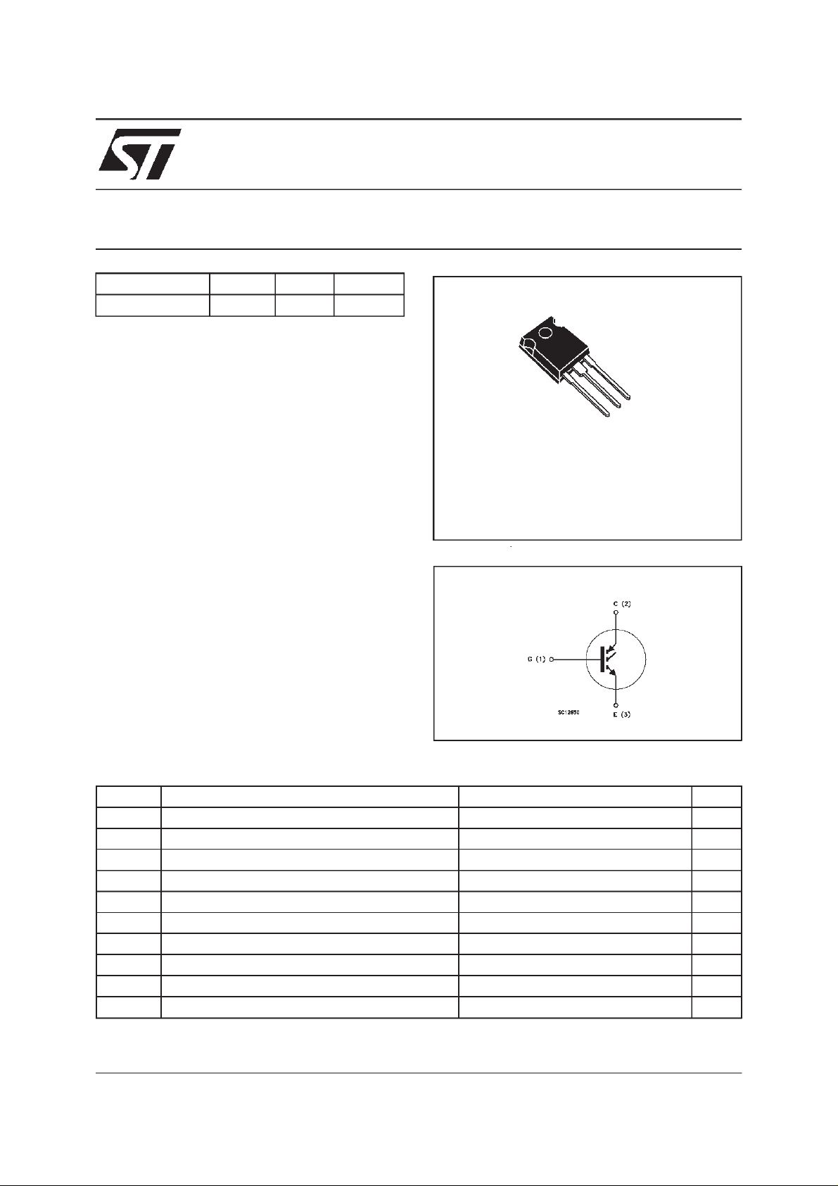
3
2
1
TO-247
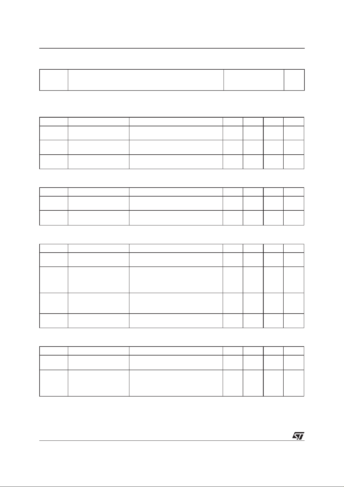
INTERNAL SCHEMATIC DIAGRAM
ABSOLUTE MAXIMUM RATINGS
Symbol Parameter Value Unit
V
V
V
I
CM
P
T
(•) Pulse width limitedby safe operatingarea
June 1999
Collect o r -Em i t t er Voltage (VGS= 0) 600 V
CES
Emit t er-Coll ect or Voltage 20 V
ECR
Gate-Emitter Voltage
GE
I
Collect o r Current (continuous) at Tc=25oC24A
C
I
Collect o r Current (continuous) at Tc= 100oC12A
C
20 V
±
(•) Collect o r Current (pulsed) 96 A
Tot al Diss i pat ion at Tc=25oC 120 W
tot
Derat ing Factor 0.96 W/
Sto rage Temperature -65 to 150
stg
T
Max. O perating Junction T emperature 150
j
o
C
o
C
o
C
1/8
Page 2
STGW12NB60H
THERMAL DATA
R
thj-case
R
thj-amb
R
thc-h
Ther mal Resistanc e Junct ion-case Max
Ther mal Resistanc e Junct ion-ambie nt Max
Ther mal Resistanc e Case-heatsink Typ
1.04
30
0.1
o
C/W
oC/W
o
C/W
ELECTRICAL CHARACTERISTICS
=25oC unless otherwisespecified)
(T
j
OFF
Sym bol Param e t er Test Condition s Min . Typ. Max. Unit
V
BR(CES)
Collector-Emitter
IC=250µAVGE= 0 600 V
Break dow n V o lt age
I
I
CES
GES
Collect o r cut- off
=0)
(V
GE
Gat e- Em i t t er Leak age
Current (V
CE
=0)
V
=MaxRating Tj=25oC
CE
=MaxRating Tj=125oC
V
CE
V
= ± 20 V VCE=0 ±100 nA
GE
10
100
ON(∗)
Sym bol Param e t er Test Condition s Min . Typ. Max. Unit
V
GE(th)
Gate Threshold
VCE=VGEIC= 250 µA35V
Voltage
V
CE(SAT)
Collector-Emitter
Sat urat ion Voltage
VGE=15V IC=12A
V
=15V IC=12A Tj= 125oC
GE
2.0
1.7
2.8 V
DYNAMIC
Sym bol Param e t er Test Condition s Min . Typ. Max. Unit
C
C
C
Q
Q
g
Q
I
CL
Forward
fs
Tr ansc on duc tance
Input Capaci t anc e
ies
Out put Capac it ance
oes
Reverse Tr ansfer
res
Capacit a nc e
Tot al Gate Charge
G
Gate-Emitt er Charge
GE
Gat e- Col lect or C harge
GC
Latc hing C urrent V
VCE=25 V IC=12A 9.5 S
VCE=25V f=1MHz VGE= 0 950
120
27
VCE= 480 V IC=12A VGE=15V 68
10
30
=480 RG=10 Ω
clamp
T
= 150oC
j
48 A
µA
µ
V
pF
pF
pF
nC
nC
nC
A
SWITCHINGON
Sym bol Param e t er Test Condition s Min . Typ. Max. Unit
(di/dt)
2/8
t
d(on)
E
Delay T ime
t
Rise Tim e
r
Tur n-on Current Slope
on
Turn-on
on
Switching Losses
VCC= 480 V IC=12A
=15V RG=10Ω
V
GE
VCC=480V IC=12A
=10Ω VGE=15V
R
G
T
=125oC
j
5
46
1000
290
ns
ns
A/µs
J
µ
Page 3
STGW12NB60H
ELECTRICAL CHARACTERISTICS
(continued)
SWITCHINGOFF
Sym bol Param e t er Test Condition s Min . Typ. Max. Unit
t
tr(v
t
d(off
E
off
E
t
tr(v
t
d(off
E
off
E
(•) Pulse width limited by max. junction temperature
(∗) Pulsed: Pulse duration = 300 µs, duty cycle 1.5 %
(**)Losses Include Also The Tail (Jedec Standardization)
Cross-O ver Time
c
Off Voltage Rise Time
)
off
)
Delay T ime
t
Fall T ime
f
(**)
Turn-off Switching Loss
Tot al Switching Los s
ts
Cross-O ver Time
c
)
Off Voltage Rise Time
off
)
Delay T ime
t
Fall T ime
f
(**)
Turn-off Switching Loss
Tot al Switching Los s
ts
VCC=480V IC=12A
R
GE
=10
Ω
VGE=15V
VCC=480V IC=12A
R
GE
= 125oC
T
j
=10
Ω
VGE=15V
150
27
76
92
0.21
0.49
230
76
95
200
0.45
0.74
ns
ns
ns
ns
mJ
mJ
ns
ns
ns
ns
mJ
mJ
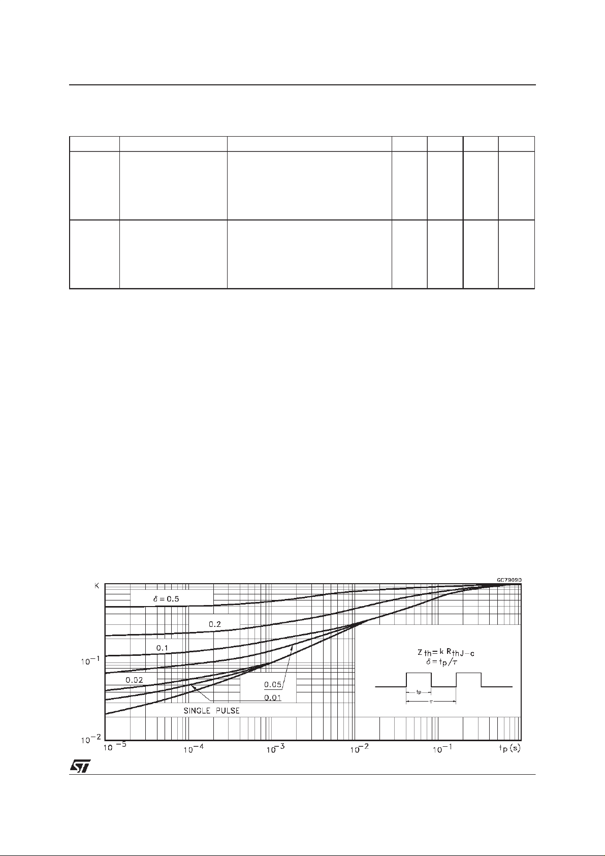
ThermalImpedance
3/8
Page 4

STGW12NB60H
OutputCharacteristics
Transconductance
TransferCharacteristics
Collector-EmitterOn Voltage vs Temperature
Collector-EmitterOn Voltage vs Collector Current
4/8
Gate Threshold vs Temperature
Page 5

STGW12NB60H
NormalizedBreakdownVoltagevs Temperature
Gate Chargevs Gate-EmitterVoltage
CapacitanceVariations
TotalSwitching Losses vs Gate Resistance
TotalSwitching Losses vs Temperature
TotalSwitching Losses vs Collector Current
5/8
Page 6

STGW12NB60H
SwitchingOff Safe Operating Area
Fig. 1: Gate Chargetest Circuit Fig. 2: TestCircuit For InductiveLoad Switching
Fig. 3
: SwitchingWaveforms
6/8
Page 7

TO-247 MECHANICAL DATA
STGW12NB60H
DIM.
MIN. TYP. MAX. MIN. TYP. MAX.
A 4.7 5.3 0.185 0.209
D 2.2 2.6 0.087 0.102
E 0.4 0.8 0.016 0.031
F 1 1.4 0.039 0.055
F3 2 2.4 0.079 0.094
F4 3 3.4 0.118 0.134
G 10.9 0.429
H 15.3 15.9 0.602 0.626
L 19.7 20.3 0.776 0.779
L3 14.2 14.8 0.559 0.582
L4 34.6 1.362
L5 5.5 0.217
M 2 3 0.079 0.118
mm inch
P025P
7/8
Page 8

STGW12NB60H
Information furnishedis believed tobe accurate and reliable.However, STMicroelectronics assumes no responsibilityfor the consequences
of use of such information nor for any infringement of patents or other rights of third parties which may result from its use. No license is
granted by implication or otherwise under any patent or patent rights of STMicroelectronics. Specificationmentioned in this publication are
subjecttochange without notice.This publication supersedes andreplaces all information previouslysupplied.STMicroelectronics products
are not authorized for use as critical components in life support devices or systemswithout express written approval of STMicroelectronics.
The STlogo is a trademark of STMicroelectronics
1999 STMicroelectronics – Printed in Italy – All Rights Reserved
STMicroelectronics GROUP OF COMPANIES
Australia - Brazil - China - Finland - France - Germany - Hong Kong - India - Italy - Japan- Malaysia - Malta - Morocco -
8/8
Singapore - Spain - Sweden - Switzerland - United Kingdom - U.S.A.
http://www.st.com
.
 Loading...