

Page 1
®
SMALL SIGNAL NPN TRANSI STOR
Type Marking
STF42 642
■ SILICON EPI TAX IA L PLANAR N PN HIGH
VOLTAGE TRANSISTOR
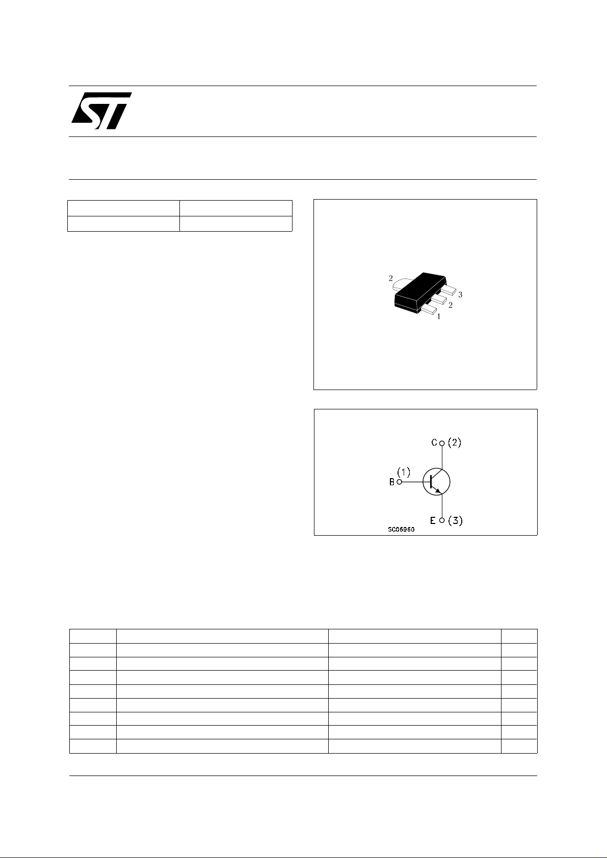
■ MINIATURE SOT-89 PLASTIC PACKAGE
FOR SURFACE MOUNTING CIRCUITS
■ TAPE AND REEL PACKING
■ THE PNP COMPLEMENTARY TYPE IS
STF92
STF42
PRELIMINARY DATA
APPLICATIONS
■ VIDEO AMPLIFIER CIRC UITS (RGB
SOT-89
CATHODE CURRENT CONTROL)
■ TELEPHONE WIRELINE INTERFACE (HOOK
SWITCHES, DIALER CIRCUITS)
INTER NAL SCH E M ATI C DIAG RA M
ABSOLUTE MAXIMUM RATINGS
Symbol Parameter Value Unit
V
V
V
I
P
T
Collector-Base Voltage (IE = 0) 300 V
CBO
Collector-Emitter Voltage (IB = 0) 300 V
CEO
Emitter-Base Voltage (IC = 0) 5 V
EBO
Collector Current 0.1 A
I
C
Collector Peak Current 0.2 A
CM
Total Dissipation at TC = 25 oC 1.3 W
tot
Storage Temperature -65 to 150
stg
Max. Operating Junction Temperature 150
T
j
o
C
o
C
May 2002
1/4
Page 2

STF42
THERMAL DATA
R
• Device mounted on a PCB area of 1 cm
• Thermal Resistance Junction-Ambient Max 96.1
thj-amb
o
2
C/W
ELECTRICAL CHARACTERISTICS (T
= 25 oC unless otherwise specified)
case
Symbol Parameter Test Conditions Min. Typ. Max. Unit
I
CBO
I
EBO
V
(BR)CBO
Collector Cut-off
Current (I
= 0)
E
Emitter Cut-off Current
(I
= 0)
C
Collector-Base
= 200 V
V
CB
V
= 200 V TC = 150 oC
CB
V
= 300 V
CB
= 5 V 50 nA
V
EB
= 100 µA
I
C
300 V
10
10
100
Breakdown Voltage
(I
= 0)
E
V
(BR)CEO
∗ Collector-Emitter
I
= 10 mA 300 V
C
Breakdown Voltage
(I
= 0)
B
V
(BR)EBO
Emitter-Base
= 100 µA
I
E
5V
Breakdown Voltage
(I
= 0)
C
V
∗ Collector-Emitter
CE(sat)
IC = 30 mA IB = 5 mA 0.6 V
Saturation Voltage
V
∗ Base-Emitter
BE(sat)
IC = 30 mA IB = 5 mA 1.2 V
Saturation Voltage
h
∗ DC Current Gain IC = 30 mA VCE = 10 V 75
FE
f
C
CBO
Transition Frequency IC = 15 mA VCE = 10 V f = 20 MHz 60 MHz
T
Collector-Base
IE = 0 VCB = 10 V f = 1 MHz 6 pF
Capacitance
C
EBO
Emitter-Base
IC = 0 VEB = 2 V f = 1 MHz 22 pF
Capacitance
∗ Pulsed: Pulse duration = 300 µs, duty cycle ≤ 1.5 %
nA
µA
µA
2/4
Page 3

SOT-89 MECHANICAL DATA
STF42
DIM.
MIN. TYP. MAX. MIN. TYP. MAX.
A 1.4 1.6 55.1 63.0
B 0.44 0.56 17.3 22.0
B1 0.36 0.48 14.2 18.9
C 0.35 0.44 13.8 17.3
C1 0.35 0.44 13.8 17.3
D 4.4 4.6 173.2 181.1
D1 1.62 1.83 63.8 72.0
E 2.29 2.6 90.2 102.4
e 1.42 1.57 55.9 61.8
e1 2.92 3.07 115.0 120.9
H 3.94 4.25 155.1 167.3
L 0.89 1.2 35.0 47.2
mm mils
P025H
3/4
Page 4

STF42
Information furnished is believed to be accurate and reliable. However, STMicroelectronics assumes no responsibility for the consequences
of use of such inform ation nor for any infringe ment o f patents or other rig hts o f third par ties which ma y resul t from i ts use. N o li cen se is
granted by implicatio n or otherwise un der any patent or patent rights of STMicroelectronics. Specification mentioned in this publication are
subject to change without notice. This publication supersedes and replaces all information previously supplied. STMicroelectronics products
are not authorized for use as critical compo nents in life support devices or systems without express written approval of STMicroelectronics.
The ST logo is a trademark of STMicroelectronics
© 2002 STMicroelectro nics – Printed in Italy – All Rights Reserved
STMicroelectronics GROUP OF COMPANIES
Australia - Brazil - Canada - China - Finland - France - Germany - Hong Kong - India - Israel - Italy - Japan - Malaysia - Malta - Morocco -
Singapore - Spain - Sweden - Switzerland - United Kingdom - United States.
http://www.st.com
4/4
 Loading...