

Page 1
STD17NE03L
N - CHANNEL 30V - 0.034Ω - 17A - DPAK/IPAK
STripFET POWER MOSFET
TYPE V
DSS
R
DS(on)
I
D
ST D1 7NE03L 30 V < 0.05 Ω 17 A
■ TYPICALR
■ EXCEPTIONAL dv/dt CAPABILITY
■ 100%AVALANCHETESTED
■ APPLICATIONORIENTED
DS(on)
= 0.034 Ω
CHARACTERIZATION
■ ADDSUFFIX ”T4” FORORDERING INTAPE
& REEL
DESCRIPTION
This Power MOSFET is the latest developmentof
STMicroelectronics unique ”Single Feature
Size” strip-based process. The resulting transistor shows extremely high packing density for
low on-resistance, rugged avalanche characteristicsand less critical alignmentsteps therefore
a remarkablemanufacturingreproducibility.
APPLICATIONS
■ SOLENOIDAND RELAYDRIVERS
■ MOTORCONTROL, AUDIO AMPLIFIERS
■ DC-DCCONVERTERS
■ AUTOMOTIVE ENVIRONMENT
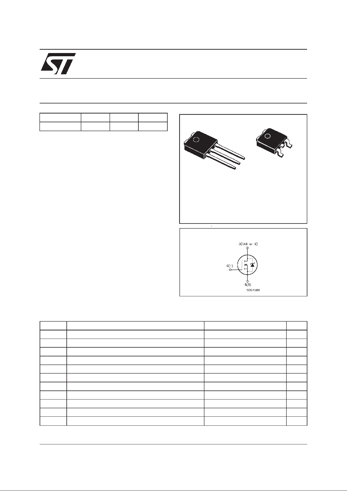
3
1
2
1
IPAK
TO-251
(Suffix”-1”)
DPAK
TO-252
(Suffix ”T4”)
INTERNAL SCHEMATIC DIAGRAM
3
ABSOLUTE MAXIMUM RATINGS
Symbol Parameter Value Unit
V
V
V
I
DM
P
dv/ dt Peak Diode Recovery voltage slope 6 V/ns
T
(•) Pulse width limited by safeoperating area (1)I
June 1999
Drain-source Voltage (VGS=0) 30 V
DS
Dra in- gate Voltage (RGS=20kΩ)
DGR
Gate -sourc e Vo ltage
GS
I
Drain Current (co ntinuous) at Tc=25oC17A
D
I
Drain Current (co ntinuous) at Tc=100oC12A
D
30 V
20 V
±
(•) Drain C urrent (pulsed) 68 A
Total Dissipation at Tc=25oC35W
tot
Derating Factor 0.23 W/
St orage Temperature -65 to 175
stg
T
Max. Op erating Junc tion Te mperature 175
j
≤
17 A, di/dt≤300 A/µs, V
SD
DD
≤
V
(BR)DSS,Tj
≤
T
JMAX
o
C
o
C
o
C
1/9
Page 2
STD17NE03L
THERMAL DATA
R
thj-case
Rthj-amb
R
thc-sink
T
AVALANCHE CHARACTERISTICS
Symbol Para meter Max V al ue Uni t
I
AR
E
Ther mal Resist ance Junction-c ase Max
Ther mal Resist ance Junction-am b ient Max
Thermal Resistance Case-sink Typ
Maximum Lead Temperature Fo r S old er ing Pur p ose
l
Avalanche Current, Re petitive or No t -Repetit ive
(pulse width limited by T
Single Pulse Avalanche En ergy
AS
(starting T
=25oC, ID=IAR,VDD=25V)
j
max)
j
4.28
100
1.5
275
17 A
50 mJ
o
C/W
oC/W
o
C/W
o
C
ELECTRICAL CHARACTERISTICS (T
=25oC unless otherwisespecified)
case
OFF
Symbol Parameter Test Conditions Min. Typ. Max. Unit
V
(BR)DSS
Drain-source
=250µAVGS=0
I
D
30 V
Break d own V o lt age
I
DSS
I
GSS
Zero Gate Voltage
Drain Cu rr ent (V
GS
Gat e- b ody Le aka ge
Current ( V
DS
=0)
=0)
V
=MaxRating
DS
= Max Rating Tc=125
V
DS
o
C
= ± 20 V
V
GS
1
10
± 100 nA
ON(∗)
Symbol Parameter Test Conditions Min. Typ. Max. Unit
V
GS(th)
Gate Threshold
V
DS=VGSID
= 250 µ A
11.72.5V
Voltage
R
DS(on)
I
D(on)
Static Drain-source On
Resistance
VGS=10V ID=8.5A
=10V ID=8.5A
V
GS
On State Dra in Current VDS>I
D(on)xRDS(on )max
0.034
0.049
17 A
0.05
0.06
VGS=10V
DYNAMIC
µA
µ
Ω
A
Symbol Parameter Test Conditions Min. Typ. Max. Unit
g
(∗)Forward
fs
VDS>I
D(on)xRDS(on )maxID
=8.5 A 5 11 S
Tr ansconductance
C
C
C
Input Cap ac i t an c e
iss
Out put Capacitance
oss
Reverse Transfer
rss
VDS=25V f=1MHz VGS=0 680
160
60
Capacitance
2/9
pF
pF
pF
Page 3
STD17NE03L
ELECTRICAL CHARACTERISTICS
(continued)
SWITCHING ON
Symbol Parameter Test Conditions Min. Typ. Max. Unit
t
d(on)
Q
Q
Q
Turn-on delay Time
t
Rise Time
r
Total Gate Charge
g
Gat e- Source Charge
gs
Gate-Drain Charge
gd
VDD=15V ID=10A
=4.7 Ω VGS=5V
R
G
VDD=24V ID=22A VGS=5V 13
15
70
18 nC
6
6
SWITCHING OFF
Symbol Parameter Test Conditions Min. Typ. Max. Unit
t
r(Voff)
t
t
Off -voltage Rise T ime
Fall Time
f
Cross-over Ti m e
c
VDD=24V ID=20A
=4.7 Ω VGS=5V
R
G
13
33
55
SOURCEDRAIN DIODE
Symbol Parameter Test Conditions Min. Typ. Max. Unit
I
SD
I
SDM
V
SD
t
Q
I
RRM
(∗) Pulsed:Pulse duration = 300µs, dutycycle 1.5%
(•) Pulse width limited by safeoperating area
Source-drain Curr ent
(•)
Source-drain Curr ent
17
68
(pulsed)
(∗) F orward On Voltage ISD=17A VGS=0 1.5 V
Reverse R ec o v ery
rr
Time
Reverse R ec o v ery
rr
= 22 A di/dt = 100 A/µs
I
SD
=15V Tj= 150oC
V
DD
40
0.45
Charge
Reverse R ec o v ery
2.2
Current
ns
ns
nC
nC
ns
ns
ns
A
A
ns
nC
A
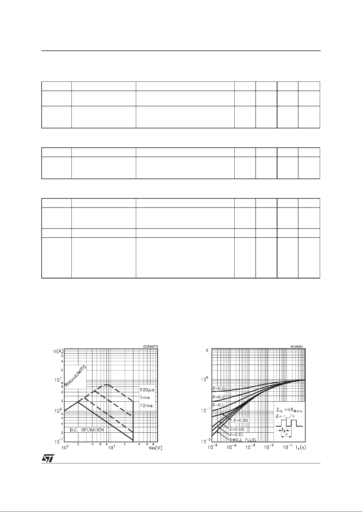
SafeOperating Area Thermal Impedance
3/9
Page 4

STD17NE03L
OutputCharacteristics
Transconductance
TransferCharacteristics
Static Drain-sourceOn Resistance
Gate Charge vs Gate-sourceVoltage
4/9
CapacitanceVariations
Page 5

STD17NE03L
Normalized GateThreshold Voltagevs
Temperature
Source-drainDiode Forward Characteristics
Normalized On Resistance vs Temperature
5/9
Page 6

STD17NE03L
Fig. 1:
UnclampedInductive LoadTest Circuit
Fig. 3: SwitchingTimes Test CircuitsFor
ResistiveLoad
Fig. 2:
UnclampedInductiveWaveform
Fig. 4: Gate Charge test Circuit
Fig. 5:
Test Circuit For InductiveLoad Switching
And Diode Recovery Times
6/9
Page 7

TO-252 (DPAK) MECHANICALDATA
STD17NE03L
DIM.
mm inch
MIN. TYP. MAX. MIN. TYP. MAX.
A 2.2 2.4 0.086 0.094
A1 0.9 1.1 0.035 0.043
A2 0.03 0.23 0.001 0.009
B 0.64 0.9 0.025 0.035
B2 5.2 5.4 0.204 0.212
C 0.45 0.6 0.017 0.023
C2 0.48 0.6 0.019 0.023
D 6 6.2 0.236 0.244
E 6.4 6.6 0.252 0.260
G 4.4 4.6 0.173 0.181
H 9.35 10.1 0.368 0.397
L2 0.8 0.031
L4 0.6 1 0.023 0.039
H
A
E
C2
L2
B2
==
==
DETAIL”A”
D
2
13
L4
A1
C
A2
DETAIL”A”
B
G
==
0068772-B
7/9
Page 8

STD17NE03L
TO-251(IPAK) MECHANICAL DATA
DIM.
MIN. TYP. MAX. MIN. TYP. MAX.
mm inch
A 2.2 2.4 0.086 0.094
A1 0.9 1.1 0.035 0.043
A3 0.7 1.3 0.027 0.051
B 0.64 0.9 0.025 0.031
B2 5.2 5.4 0.204 0.212
B3 0.85 0.033
B5 0.3 0.012
B6 0.95 0.037
C 0.45 0.6 0.017 0.023
C2 0.48 0.6 0.019 0.023
D 6 6.2 0.236 0.244
E 6.4 6.6 0.252 0.260
G 4.4 4.6 0.173 0.181
H 15.9 16.3 0.626 0.641
L 9 9.4 0.354 0.370
L1 0.8 1.2 0.031 0.047
L2 0.8 1 0.031 0.039
H
8/9
A
E
==
C2
L2
B2
==
D
B3
2
13
L1
B6
A1
C
A3
L
B
B5
G
==
0068771-E
Page 9

STD17NE03L
Information furnished is believed tobeaccurateand reliable. However, STMicroelectronics assumesno responsibility for the consequences
of use of such information nor for any infringement of patents or other rights of third parties which may resultfrom its use. No license is
granted by implication or otherwise under any patent or patent rights of STMicroelectronics. Specificationmentioned in this publicationare
subjecttochange without notice.Thispublication supersedesand replacesall information previouslysupplied.STMicroelectronics products
are not authorizedfor useas critical components in lifesupport devices or systems without express written approval of STMicroelectronics.
The STlogo is a trademark of STMicroelectronics
1999 STMicroelectronics – Printed in Italy – All Rights Reserved
STMicroelectronics GROUP OF COMPANIES
Australia - Brazil - Canada - China -France - Germany - Italy- Japan- Korea- Malaysia - Malta - Mexico - Morocco - The Netherlands -
Singapore - Spain - Sweden - Switzerland - Taiwan- Thailand - UnitedKingdom - U.S.A.
http://www.st.com
.
9/9
 Loading...