

Page 1
STD17N05L
STD17N06L
N - CHANNEL ENHANCEMENT MODE
LOW THRESHOLD POWER MOS TRANSISTOR
TYPE V
DSS
R
DS(on)
I
D
STD 17N05L 50 V < 0. 085 Ω 17 A
STD 17N06L 60 V < 0. 085 Ω 17 A
■ TYPICAL R
■ AVALANCHE RUGGED TECHNOLOGY
■ 100% AVALANCHE TESTED
■ REPETITIVE AVALANCHE DATA AT 100
■ LOW GATE CHARGE
■ LOGIC LEVEL COMPATIBLE INPUT
o
■ 175
■ APPLICATION ORIENTED
C OPERATING TEMPERATURE
DS(on)
= 0.065 Ω
o
C
CHARACTERIZATION
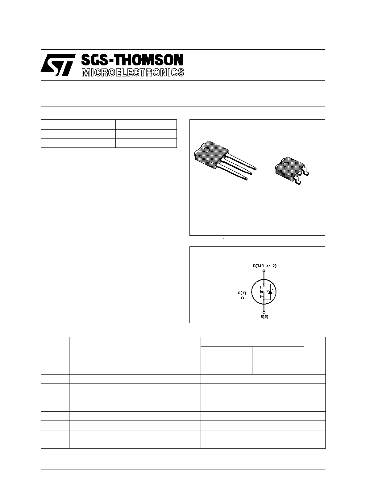
■ THROUGH-HOLE IPAK (TO-251) POWER
PACKAGE IN TUBE (SUFFIX ”-1”)
■ SURFACE-MOUNTINGDPAK (TO-252)
POWER PACKAGE IN TAPE & REEL
(SUFFIX ”T4”)
APPLICATIONS
■ HIGH CURRENT, HIGH SPEED SWITCHING
■ SOLENOID AND RELAY DRIVERS
■ REGULATORS
■ DC-DC & DC-AC CONVERTERS
■ MOTOR CONTROL, AUDIO AMPLIFIERS
■ AUTOMOTIVE ENVIRONMENT (INJECTION,
ABS, AIR-BAG, LAMPDRIVERS, Etc.)
3
2
1
IPAK
TO-251
(Suffix ”-1”)
INTERNAL SCHEMATIC DIAGRAM
1
DPAK
TO-252
(Suffix ”T4”)
3
ABSOLUTE MAXIMUM RATINGS
Symb o l Paramet er Val u e Unit
STD 17N05L STD17N06L
V
V
V
I
DM
P
T
(•) Pulsewidth limited bysafe operating area
January 1995
Drain - s ource Voltage (VGS=0) 50 60 V
DS
Drain- gate Voltage (RGS=20kΩ)5060V
DGR
Gate-source Voltage ± 15 V
GS
Drain Current (continuous) at Tc=25oC17A
I
D
Drain Current (continuous) at Tc=100oC12A
I
D
(•) Drain Current (pulsed) 68 A
Total D i ssipation at Tc=25oC55W
tot
Derating F actor 0.37 W/
St or a ge Tem perature -65 to 175
stg
Max. Operating Junctio n Temperatur e 175
T
j
o
o
o
C
C
C
1/10
Page 2
STD17N05L/STD17N06L
THERMAL DATA
R
thj-case
R
thj-amb
R
thc-sink
T
AVALANCHE CHARACTERISTICS
Symbol Parameter Max Value Uni t
I
AR
E
E
I
AR
Thermal Resistance Junction - cas e Max
Thermal Resistance Junction- ambient Max
Thermal Resistance Case-sink Typ
Maximum Lead T emperature For Soldering Purp ose
l
Avalanc h e Cu rr ent , Repet itive or Not-R epetitive
(pulse width limited by Tjmax, δ <1%)
Single Pul se Avalanche Ener gy
AS
(starti ng Tj=25oC, ID=IAR,VDD=25V)
Repetitive Avalanc he Energ y
AR
(pulse width limited by Tjmax, δ <1%)
Avalanc h e Cu rr ent , Repet itive or Not-R epetitive
(Tc= 100oC, puls e width limited by Tjmax, δ <1%)
2.73
100
1.5
275
17 A
60 mJ
15 mJ
12 A
o
C/W
o
C/W
o
C/W
o
C
ELECTRICAL CHARACTERISTICS (T
=25oC unless otherwise specified)
case
OFF
Symbol Parameter Test Co ndition s Min. Typ. Max. Unit
V
(BR)DSS
I
DSS
I
GSS
Drain - s ource
Break d own Volta ge
Zer o Gate Voltage
Drain Current (VGS=0)
Gat e- body Leakage
ID=250µAVGS=0
for STD17 N05L
for STD17 N06L
VDS=MaxRating
VDS= Max R ating x 0.8 Tc=125oC
50
60
250
1000µAµA
VGS= ± 15 V ± 100 nA
Current (VDS=0)
ON (∗)
Symbol Parameter Test Co ndition s Min. Typ. Max. Unit
V
GS(th)
R
DS(on)
I
D(on)
Gate Threshold Voltage VDS=VGSID=250µA11.62.5V
St at ic Drain-s our ce O n
Resistance
On St ate Dra in Current VDS>I
VGS=5V ID=8.5A
V
=5V ID=8.5A Tc= 100oC
GS
D(on)xRDS(on)max
0.065 0.085
0.17
17 A
VGS=10V
DYNAMIC
Symbol Parameter Test Co ndition s Min. Typ. Max. Unit
(∗)Forward
g
fs
Tr ansconductance
C
C
C
Input Capacitance
iss
Out put Capacitance
oss
Reverse Transfer
rss
Capacitance
VDS>I
D(on)xRDS(on)maxID
=8.5A 5 12 S
VDS=25V f=1MHz VGS=0 700
250
70
1000
350
100
V
V
Ω
Ω
pF
pF
pF
2/10
Page 3
STD17N05L/STD17N06L
ELECTRICAL CHARACTERISTICS (continued)
SWITCHING RESISTIVE LOAD
Symbol Parameter Test Co ndition s Min. Typ. Max. Unit
t
d(on)
(di/dt)
Q
Q
Q
Turn-on Time
t
Rise Time
r
Turn-on C urrent Slope VDD=40V ID=17A
on
Total Gate Charge
g
Gat e- Source Charge
gs
Gate-Drain Charge
gd
SWITCHING INDUCTIVE LOAD
Symbol Parameter Test Co ndition s Min. Typ. Max. Unit
t
r(Voff)
t
Off -voltage R ise Time
t
Fall Time
f
Cross-over Time
c
SOURCE DRAIN DIODE
VDD=30V ID=8.5A
RGS=50 Ω VGS=5V
60
35090500
(see test circuit, figure 3)
130 A/µs
RGS=50 Ω VGS=5V
(see test circuit, figure 5)
VDD=40V ID=17A VGS=5V 18
6
9
VDD=40V ID=17A
RGS=50 Ω VGS=5V
(see test circuit, figure 5)
70
100
180
26 nC
100
150
260
ns
ns
nC
nC
ns
ns
ns
Symbol Parameter Test Co ndition s Min. Typ. Max. Unit
I
I
SDM
SD
Source-drain Current
(•)
Source-drain Current
17
68
(pulsed)
V
(∗) For w ar d On Volt age ISD=17A VGS=0 1.5 V
SD
t
Reverse Recovery
rr
Time
Q
Reverse Recovery
rr
ISD= 17 A di/dt = 100 A /µs
VDD=30V Tj=150oC
(see test circuit, figure 5)
65
0.13
Charge
I
RRM
Reverse Recovery
4
Current
(∗) Pulsed:Pulse duration = 300 µs, dutycycle 1.5 %
(•) Pulse widthlimited by safeoperating area
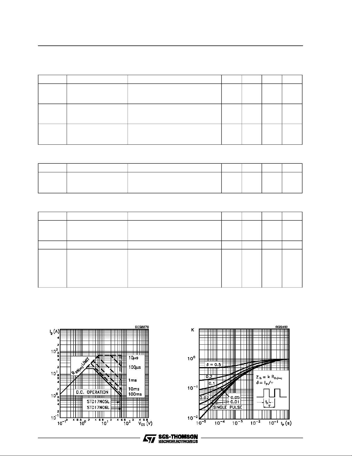
Safe Operating Area Thermal Impedance
A
A
ns
µC
A
3/10
Page 4

STD17N05L/STD17N06L
Derating Curve
Transfer Characteristics
Output Characteristics
Transconductance
Static Drain-source On Resistance
4/10
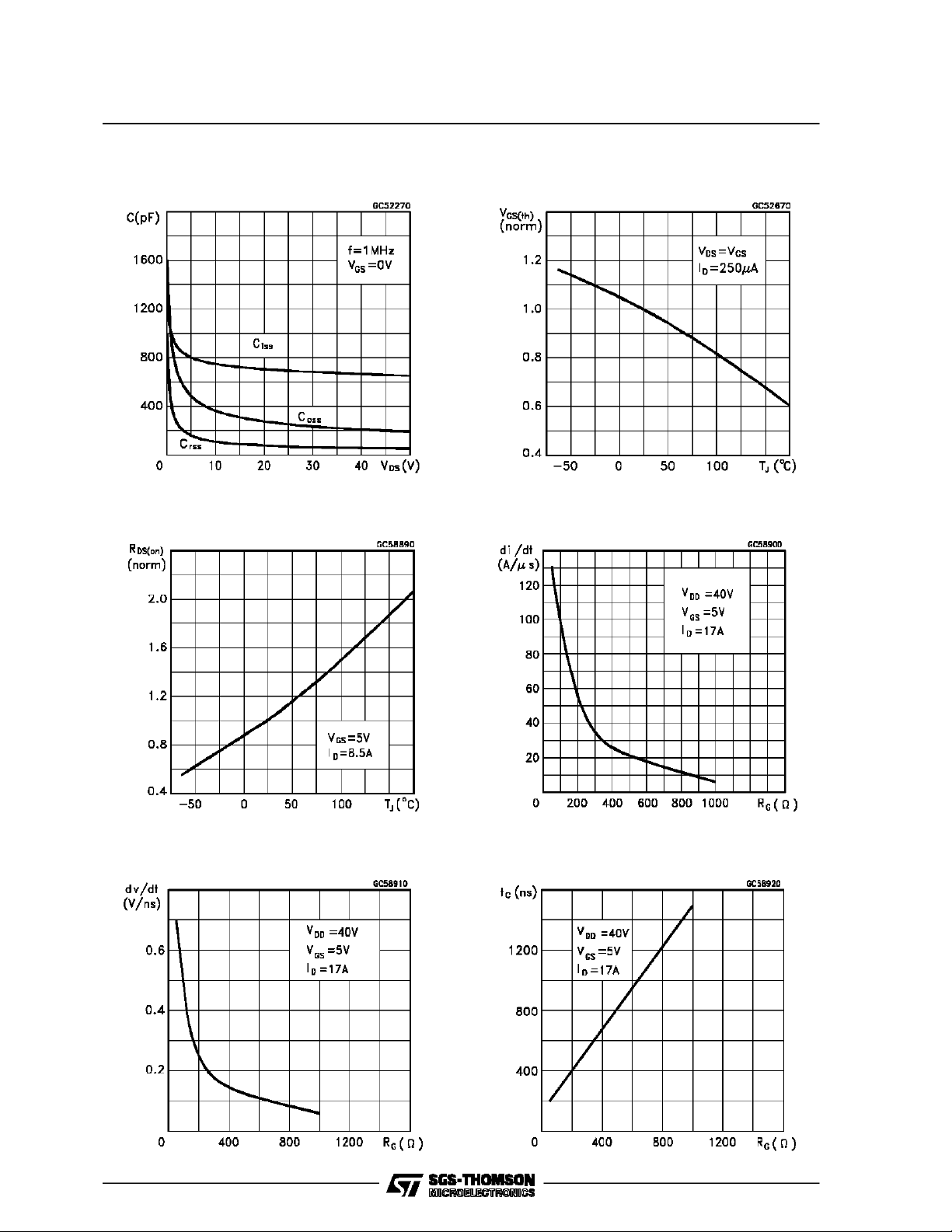
Gate Charge vs Gate-source Voltage
Page 5
STD17N05L/STD17N06L
Capacitance Variations Normalized Gate Threshold Voltage vs
Temperature
Normalized On Resistance vs Temperature Turn-on Current Slope
Cross-over TimeTurn-off Drain-source Voltage Slope
5/10
Page 6

STD17N05L/STD17N06L
Switching SafeOperating Area Accidental Overload Area
Source-drain Diode Forward Characteristics
Fig. 1: Unclamped Inductive Load Test Circuits Fig. 2: Unclamped Inductive Waveforms
6/10
Page 7

STD17N05L/STD17N06L
Fig. 3: Switching Times Test Circuits For
Resistive Load
Fig. 5: Test Circuit For Inductive Load Switching
And Diode Recovery Times
Fig. 4: Gate Charge Test Circuit
7/10
Page 8

STD17N05L/STD17N06L
TO-251 (IPAK) MECHANICAL DATA
DIM.
mm inch
MIN. TYP. MAX. MIN. TYP. MAX.
A 2.2 2.4 0.086 0.094
A1 0.9 1.1 0.035 0.043
A3 0.7 1.3 0.027 0.051
B 0.64 0.9 0.025 0.031
B2 5.2 5.4 0.204 0.212
B3 0.85 0.033
B5 0.3 0.012
B6 0.95 0.037
C 0.45 0.6 0.017 0.023
C2 0.48 0.6 0.019 0.023
D 6 6.2 0.236 0.244
E 6.4 6.6 0.252 0.260
G 4.4 4.6 0.173 0.181
H 15.9 16.3 0.626 0.641
L 9 9.4 0.354 0.370
L1 0.8 1.2 0.031 0.047
L2 0.8 1 0.031 0.039
8/10
A
E
==
C2
L2
B2
==
H
C
A3
A1
B6
L
B
B5
G
==
D
B3
2
13
L1
0068771-E
Page 9

TO-252 (DPAK)MECHANICAL DATA
STD17N05L/STD17N06L
DIM.
mm inch
MIN. TYP. MAX. MIN. TYP. MAX.
A 2.2 2.4 0.086 0.094
A1 0.9 1.1 0.035 0.043
A2 0.03 0.23 0.001 0.009
B 0.64 0.9 0.025 0.035
B2 5.2 5.4 0.204 0.212
C 0.45 0.6 0.017 0.023
C2 0.48 0.6 0.019 0.023
D 6 6.2 0.236 0.244
E 6.4 6.6 0.252 0.260
G 4.4 4.6 0.173 0.181
H 9.35 10.1 0.368 0.397
L2 0.8 0.031
L4 0.6 1 0.023 0.039
H
A
E
==
C2
L2
B2
==
DETAIL”A”
D
2
13
L4
A1
C
A2
DETAIL”A”
B
G
==
0068772-B
9/10
Page 10

STD17N05L/STD17N06L
Information furnished isbelieved to be accurateand reliable. However, SGS-THOMSONMicroelectronics assumes noresponsability for the
consequences of use of suchinformation nor for any infringementof patents orother rights of third parties whichmay results from its use. No
license isgrantedby implicationor otherwiseunder anypatentor patentrights ofSGS-THOMSON Microelectronics.Specificationsmentioned
in this publicationare subjectto change without notice.This publication supersedes and replacesall information previouslysupplied.
SGS-THOMSON Microelectronicsproducts arenotauthorizedfor useascriticalcomponents inlifesupportdevices orsystemswithout express
written approvalof SGS-THOMSON Microelectonics.
1994 SGS-THOMSONMicroelectronics - All Rights Reserved
Australia - Brazil- France - Germany -Hong Kong -Italy - Japan - Korea - Malaysia -Malta - Morocco - The Netherlands -
Singapore -Spain - Sweden- Switzerland -Taiwan - Thailand - United Kingdom -U.S.A
SGS-THOMSON Microelectronics GROUP OF COMPANIES
10/10
 Loading...