

Page 1
STB11NB40
N - CHANNEL ENHANCEMENT MODE
PowerMESH MOSFET
TYPE V
DSS
R
DS(on)
I
D
ST B11NB40 400 V < 0. 5 5 Ω 10.7 A
■ TYPICALR
■ EXTREMELY HIGH dV/dt CAPABILITY
■ 100% AVALANCHETESTED
■ VERYLOW INTRINSIC CAPACITANCES
■ GATECHARGEMINIMIZED
DS(on)
=0.48 Ω
DESCRIPTION
Using the latest high voltage MESH OVERLAY
process, SGS-Thomson has designed an
advanced family of power MOSFETs with
outstanding performances. The new patent
pending strip layout coupled with the Company’s
proprietary edge termination structure, gives the
lowest RDS(on) per area, exceptional avalanche
and dv/dt capabilities and unrivalled gate charge
and switchingcharacteristics.
APPLICATIONS
■ HIGH CURRENT, HIGH SPEEDSWITCHING
■ SWITCHMODEPOWER SUPPLIES(SMPS)
■ DC-ACCONVERTERS FORWELDING
EQUIPMENTAND UNINTERRUPTIBLE
POWERSUPPLIESAND MOTORDRIVE
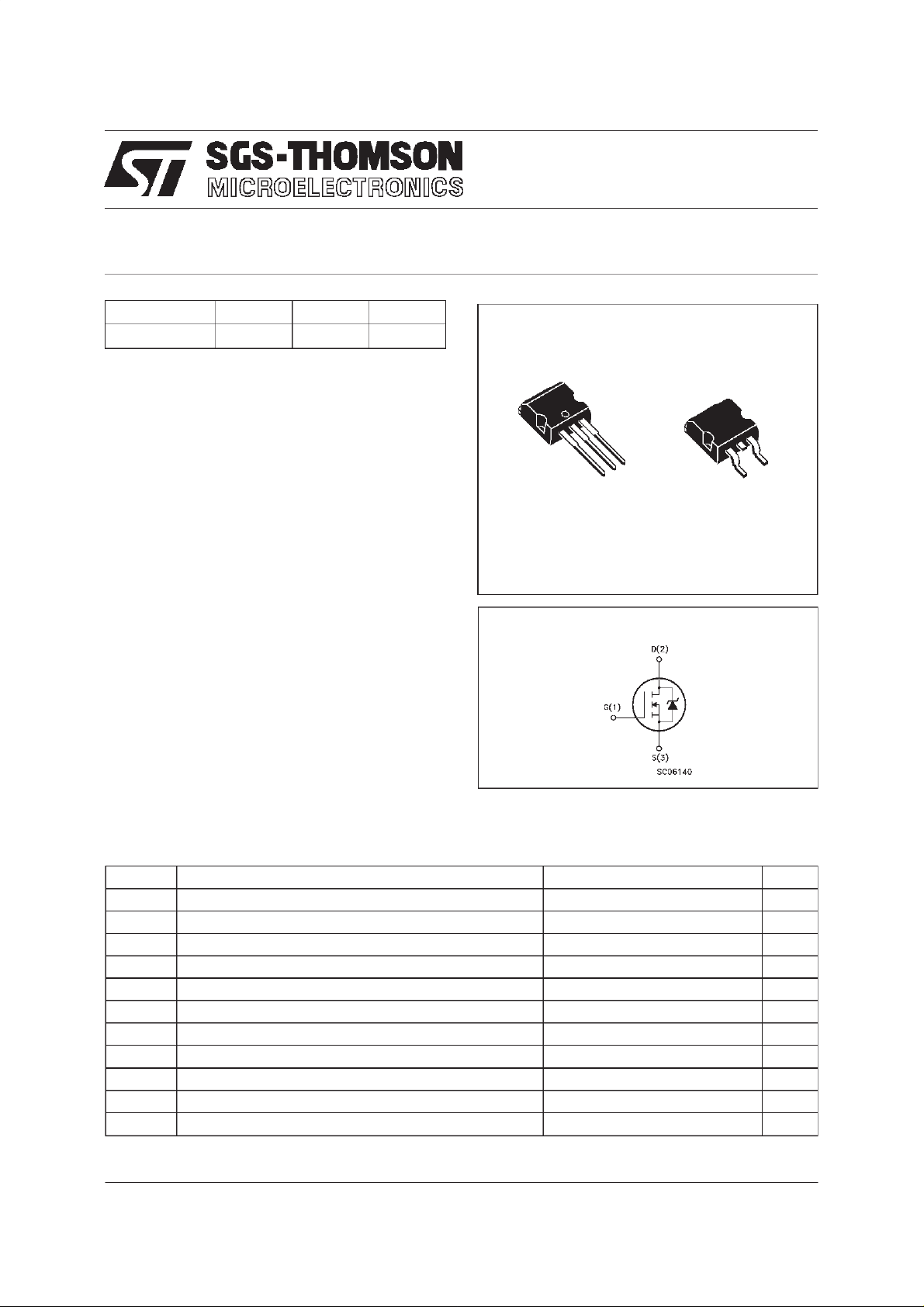
3
2
I2PAK
TO-262
(suffix ”-1”)
1
(suffix ”T4”)
1
D2PAK
TO-263
INTERNAL SCHEMATIC DIAGRAM
3
ABSOLUTE MAXIMUM RATINGS
Symb o l Para meter Value Uni t
V
V
V
I
DM
P
dv/dt(
T
(•) Pulse width limited by safe operating area (1)ISD≤ 11A, di/dt ≤ 200 A/µs, VDD≤ V
March 1998
Drain-source Volt age (VGS=0) 400 V
DS
Drain- gate Voltage ( RGS=20kΩ)
DGR
Gat e- sourc e Vo lt age ± 30 V
GS
I
Drain C urr ent ( contin uous) at Tc=25oC10.7A
D
I
Drain C urr ent ( contin uous) at Tc=100oC6.7A
D
400 V
(•) Dra in C urr ent ( pul sed) 42.8 A
Tot al Diss ip at i on at Tc=25oC125W
tot
Derating Factor 1.0 W/
1) Peak Diode Re c overy vo lt age slope 4.5 V/ns
Sto rage Tempe r ature -65 to 150
stg
T
Max. Operatin g J u nct ion T emper at u r e 150
j
,Tj≤T
(BR)DSS
JMAX
o
C
o
C
o
C
1/9
Page 2
STB11NB40
THERMAL DATA
R
thj-case
Rthj-amb
R
thc-sin k
T
AVALANCHE CHARACTERISTICS
Symbol Para met e r Max Valu e Unit
I
AR
E
Ther mal Resist ance Junctio n- case Max
Ther mal Resist ance Junctio n- ambient Max
Ther mal Resist ance Case-si nk Typ
Maximum Lea d Tempera t u re F or Sold eri ng Purpose
l
Avalanche Curre nt , Repetitive or Not-Repet it ive
(pulse w idth limited by T
Single Pulse Avalanche Energy
AS
(starting T
=25oC, ID=IAR,VDD=50V)
j
max, δ <1%)
j
1.0
62.5
0.5
300
10.7 A
530 mJ
o
C/W
oC/W
o
C/W
o
C
ELECTRICAL CHARACTERISTICS (T
=25oC unlessotherwisespecified)
case
OFF
Symbol Parameter Test Condition s Min. Typ. Ma x. Unit
V
(BR)DSS
Drain-sourc e
=250µAVGS=0
I
D
400 V
Breakdown Volt age
I
DSS
I
GSS
Zer o Gat e V o lt age
Drain Current (V
GS
Gat e-body Leak a ge
Current (V
DS
=0)
=0)
=MaxRating
V
DS
V
=MaxRating Tc=125oC
DS
= ± 30 V
V
GS
1
50
± 100 nA
ON (∗)
Symbol Parameter Test Condition s Min. Typ. Ma x. Unit
V
GS(th )
Gate Threshold
V
DS=VGSID
=250µA
345V
Voltage
R
DS(on)
Stati c Drain-so urce On
VGS=10V ID= 5.3 A 0.48 0.55 Ω
Resistance
I
D(on)
On S tate Drain Curr e nt VDS>I
D(on)xRDS(on)max
10.7 A
VGS=10V
DYNAMIC
Symbol Parameter Test Condition s Min. Typ. Ma x. Unit
g
(∗)Forward
fs
Tr ansconduc tanc e
C
C
C
Input Ca pacitan ce
iss
Out put C apa c itanc e
oss
Reverse Trans fer
rss
Capa cit an c e
VDS>I
D(on)xRDS(on)maxID
=5.3A 5 6.5 S
VDS=25V f=1MHz VGS= 0 1115
210
22
1450
280
30
µA
µA
pF
pF
pF
2/9
Page 3
STB11NB40
ELECTRICAL CHARACTERISTICS (continued)
SWITCHINGON
Symbol Parameter Test Condition s Min. Typ. Ma x. Unit
t
d(on)
Turn-on Time
r
Rise Time
t
VDD=200V ID=5.3A
=4.7 Ω VGS=10V
R
G
17
10
(see test circuit, figure 3)
Q
Q
Q
Total Gate Charge
g
Gat e-Sou rc e Cha rge
gs
Gate-Drain Charge
gd
VDD=320V ID=10.7A VGS= 10 V 29.5
10.6
11.8
SWITCHINGOFF
Symbol Parameter Test Condition s Min. Typ. Ma x. Unit
t
r(Voff)
t
t
Of f - voltag e Rise Time
Fall Time
f
Cross-ov er T ime
c
VDD=320V ID=10.7A
=4.7 Ω VGS=10V
R
G
(see test circuit, figure 5)
10
10
17
SOURCE DRAIN DIODE
Symbol Parameter Test Condition s Min. Typ. Ma x. Unit
I
SD
I
SDM
V
SD
t
Q
I
RRM
(∗) Pulsed: Pulse duration =300 µs, duty cycle1.5 %
(•) Pulse width limited by safe operating area
Source-drain Curre nt
(•)
Source-drain Curre nt
(pulsed)
(∗) For ward On Vo lt age ISD=10.7A VGS=0 1.6 V
Reverse Rec ov er y
rr
Time
Reverse Rec ov er y
rr
= 10. 7 A di/dt = 100 A /µs
I
SD
=100V Tj=150oC
V
DD
(see test circuit, figure 5)
400
3.4
Charge
Reverse Rec ov er y
17
Current
25
15
43 nC
14
14
25
10.7
42.8
ns
ns
nC
nC
ns
ns
ns
A
A
ns
µC
A
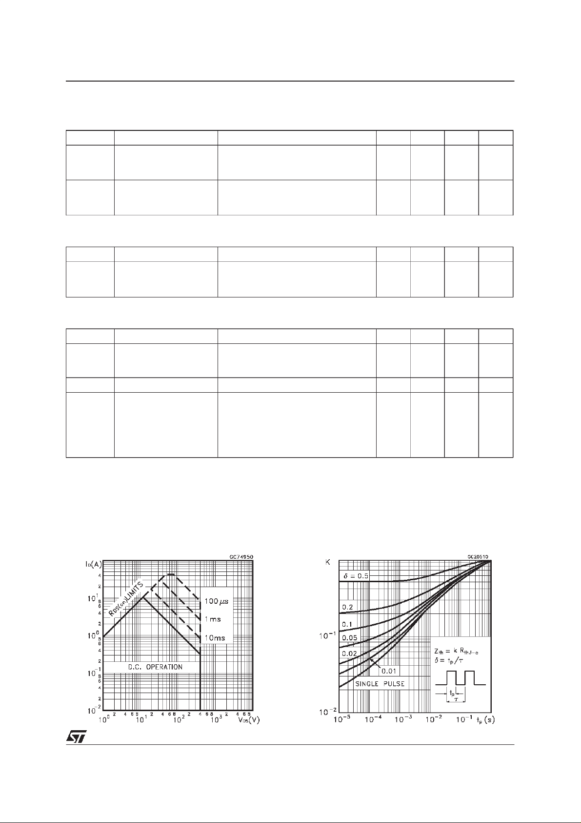
Safe Operating Area ThermalImpedance
3/9
Page 4

STB11NB40
OutputCharacteristics
Transconductance
TransferCharacteristics
StaticDrain-sourceOn Resistance
GateCharge vs Gate-sourceVoltage
4/9
CapacitanceVariations
Page 5

STB11NB40
Normalized Gate Threshold Voltage vs
Temperature
Source-drainDiode Forward Characteristics
Normalized On Resistancevs Temperature
5/9
Page 6

STB11NB40
Fig. 1: Unclamped InductiveLoad Test Circuit
Fig. 3: SwitchingTimes Test Circuits For
ResistiveLoad
Fig. 2: Unclamped Inductive Waveform
Fig. 4: Gate Chargetest Circuit
Fig. 5: Test Circuit For InductiveLoad Switching
And Diode RecoveryTimes
6/9
Page 7

TO-262(I2PAK) MECHANICAL DATA
STB11NB40
DIM.
MIN. TYP. MAX. MIN. TYP. MAX.
A 4.3 4.6 0.169 0.181
A1 2.49 2.69 0.098 0.106
B 0.7 0.93 0.027 0.036
B1 1.2 1.38 0.047 0.054
B2 1.25 1.4 0.049 0.055
C 0.45 0.6 0.017 0.023
C2 1.21 1.36 0.047 0.053
D 8.95 9.35 0.352 0.368
e 2.44 2.64 0.096 0.104
E 10 10.28 0.393 0.404
L 13.2 13.5 0.519 0.531
L1 3.48 3.78 0.137 0.149
L2 1.27 1.4 0.050 0.055
mm inch
CA1
A
C2
B2
B
e
E
L1
L2
D
L
P011P5/C
7/9
Page 8

STB11NB40
TO-263 (D2PAK) MECHANICAL DATA
DIM.
MIN. TYP. MAX. MIN. TYP. MAX.
A 4.3 4.6 0.169 0.181
A1 2.49 2.69 0.098 0.106
B 0.7 0.93 0.027 0.036
B2 1.25 1.4 0.049 0.055
C 0.45 0.6 0.017 0.023
C2 1.21 1.36 0.047 0.053
D 8.95 9.35 0.352 0.368
E 10 10.28 0.393 0.404
G 4.88 5.28 0.192 0.208
L 15 15.85 0.590 0.624
L2 1.27 1.4 0.050 0.055
L3 1.4 1.75 0.055 0.068
mm inch
E
A
C2
L2
D
L
L3
B2
B
A1
C
G
P011P6/C
8/9
Page 9

STB11NB40
Information furnished is believed to be accurate and reliable. However, SGS-THOMSON Microelectronics assumes no responsability for the
consequences of use of such information nor for anyinfringementofpatents or other rightsof third parties which may results from itsuse. No
license is granted by implication or otherwise underanypatent orpatent rights of SGS-THOMSON Microelectronics. Specifications mentioned
in thispublication are subject to change without notice. This publication supersedes and replaces all information previously supplied.
SGS-THOMSON Microelectronics productsarenot authorizedforuseas criticalcomponentsinlifesupport devices orsystems without express
written approval ofSGS-THOMSON Microelectonics.
1998 SGS-THOMSON Microelectronics - Printedin Italy - All Rights Reserved
Australia - Brazil - Canada -China - France - Germany- Italy - Japan- Korea - Malaysia - Malta- Morocco - The Netherlands -
Singapore - Spain - Sweden- Switzerland - Taiwan -Thailand - United Kingdom - U.S.A
SGS-THOMSON Microelectronics GROUP OF COMPANIES
...
9/9
 Loading...