

Page 1
STB10NB20
N - CHANNEL200V - 0.30Ω - 10A - D2PAK
PowerMESH MOSFET
TYPE V
DSS
R
DS(on)
I
D
ST B10NB20 200 V < 0.40 Ω 10 A
■ TYPICALR
■ EXTREMELYHIGH dv/dt CAPABILITY
■ 100%AVALANCHETESTED
■ VERYLOW INTRINSIC CAPACITANCES
■ GATECHARGE MINIMIZED
■ FORTHROUGH-HOLE VERSIONCONTACT
DS(on)
= 0.30 Ω
SALESOFFICE
DESCRIPTION
Using the latest high voltage MESH OVERLAY
process, STMicroelectronis has designed an
advanced family of power MOSFETs with
outstanding performances. The new patent
pending strip layout coupled with the Company’s
proprietary edge termination structure, gives the
lowest RDS(on) per area, exceptional avalanche
and dv/dt capabilities and unrivalled gate charge
and switching characteristics.
APPLICATIONS
■ HIGHCURRENT, HIGH SPEEDSWITCHING
■ SWITCHMODE POWER SUPPLIES (SMPS)
■ DC-AC CONVERTERS FOR WELDING
EQUIPMENTANDUNINTERRUPTIBLE
POWERSUPPLIESAND MOTORDRIVE
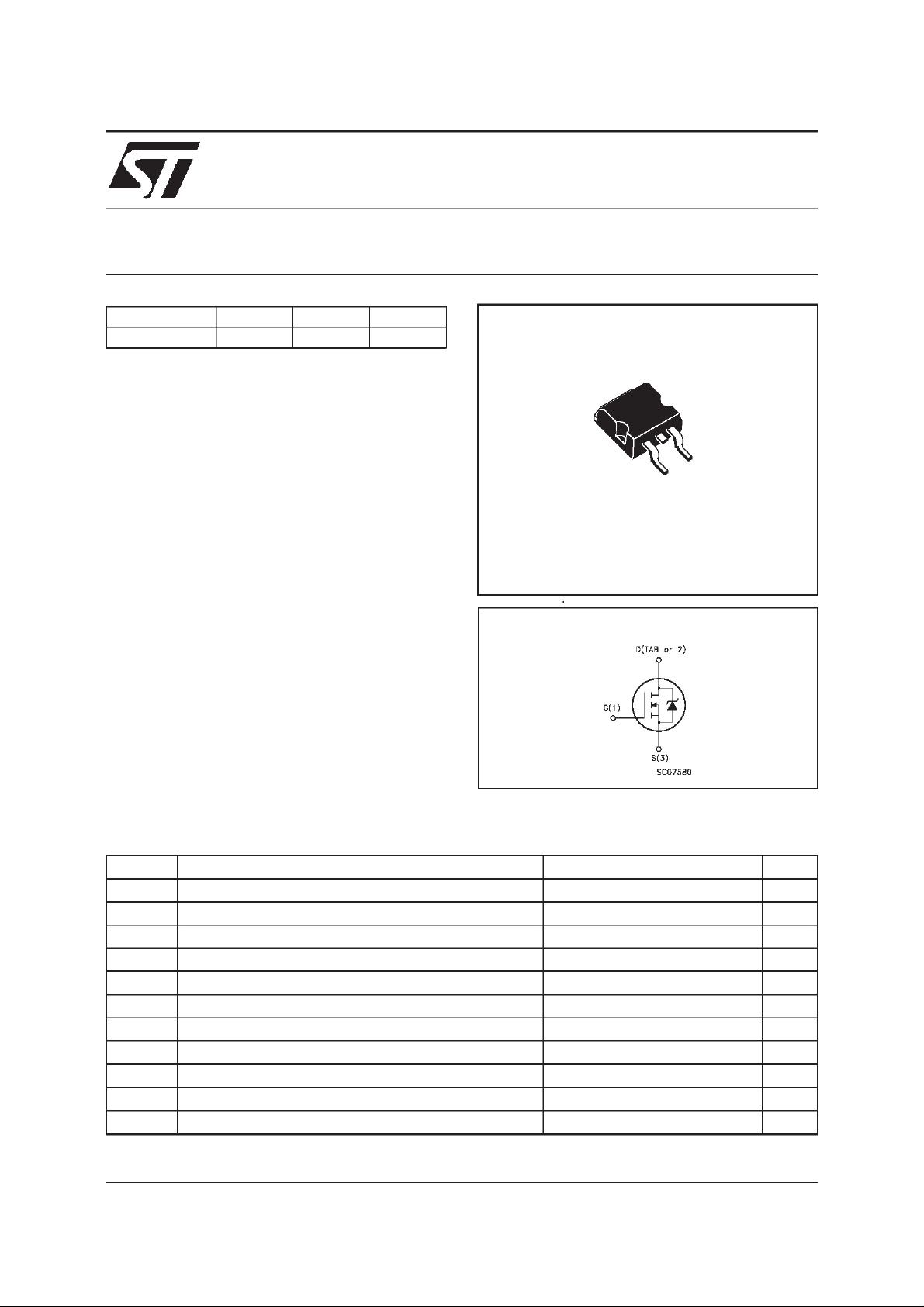
3
1
D2PAK
TO-263
(suffix ”T4”)
INTERNAL SCHEMATIC DIAGRAM
ABSOLUTE MAXIMUM RATINGS
Symb o l Parameter Val u e Uni t
V
V
V
I
DM
P
dv/dt(
T
(•) Pulse width limited by safe operatingarea (1)ISD≤ 10A, di/dt ≤ 300A/µs,VDD≤ V
November 1998
Drain-source V o lt age (VGS=0) 200 V
DS
Drain- gate Vol ta ge (RGS=20kΩ)200V
DGR
Gate-s ource Voltage ± 30 V
GS
I
Drain Curr ent (c ont i nuous) at Tc=25oC10A
D
I
Drain Curr ent (c ont i nuous) at Tc= 100oC6A
D
(•) Drain Current ( pulsed) 40 A
Total Dissipation at Tc=25oC85W
tot
Derating Fact or 0.68 W/
1) Peak D iode Recove r y vo lt age s lope 5.5 V/ ns
St orage Temperature -65 to 150
stg
T
Max. O per ating Jun ct ion Temp erat ure 150
j
,Tj≤T
(BR)DSS
JMAX
o
C
o
C
o
C
1/8
Page 2
STB10NB20
THERMAL DATA
R
thj-case
Rthj-a mb
R
thc-sink
T
AVALANCHE CHARACTERISTICS
Symbol Parameter Max Value Unit
I
AR
E
Ther mal Resistanc e Junct ion-case Max
Ther mal Resistanc e Junct ion-ambie nt Max
Ther mal Resistanc e Case-sink Ty p
Maximum Lead Te m pe ra t ure For Soldering Purpos e
l
Avalanche Current, Repetitive or Not-Repetitive
(pulse width limited by T
Single P ul se Avalanche E ner gy
AS
(starting T
=25oC, ID=IAR,VDD=50V)
j
max)
j
1.47
62.5
0.5
300
10 A
150 mJ
o
C/W
oC/W
o
C/W
o
C
ELECTRICAL CHARACTERISTICS
=25oC unless otherwisespecified)
(T
case
OFF
Symbol Parameter Test Conditions Min. Typ. M ax. Unit
V
(BR)DSS
Drain-source
ID=250µAVGS= 0 200 V
Break dow n Voltage
I
DSS
I
GSS
Zero Gate Voltage
Drain Cur re nt ( V
GS
Gat e- bod y L eakage
Current (V
DS
=0)
=0)
V
=MaxRating
DS
=MaxRating Tc=125oC
V
DS
V
=± 30 V
GS
1
10
100 nA
±
ON (∗)
Symbol Parameter Test Conditions Min. Typ. M ax. Unit
V
GS(th)
R
DS(on)
Gate Threshold Voltage VDS=VGSID= 250 µA 345V
Sta t ic Drain -s ource On
VGS=10V ID= 5 A 0.30 0.40
Resistance
I
D(on)
On State Drain Current VDS>I
D(on)xRDS(on)max
10 A
VGS=10V
DYNAMIC
Symbol Parameter Test Conditions Min. Typ. M ax. Unit
g
(∗)Forward
fs
Tr ansc on duc tance
C
C
C
Input Capac i t ance
iss
Out put Capacitance
oss
Reverse Tr ansfer
rss
Capacit a nc e
VDS>I
D(on)xRDS(on)maxID
=5 A 3 4 S
VDS=25V f=1MHz VGS= 0 470
135
22
650
190
30
µ
µA
Ω
pF
pF
pF
A
2/8
Page 3
STB10NB20
ELECTRICAL CHARACTERISTICS
(continued)
SWITCHING ON
Symbol Parameter Test Conditions Min. Typ. M ax. Unit
t
d(on)
t
r
Turn-on Time
Rise Ti me
VDD=100V ID=5A
R
=4.7
G
Ω
VGS=10V
10
15
14
20
(see test circuit, figure 3)
Q
Q
Q
Tot al Gat e Charge
g
Gat e- Source Charge
gs
Gate-Drain Charge
gd
VDD= 160 V ID=10A VGS=10V 17
7.5
5.5
24 nC
SWITCHING OFF
Symbol Parameter Test Conditions Min. Typ. M ax. Unit
t
r(Voff)
t
t
Off-voltage Rise T ime
Fall T ime
f
Cross-over Time
c
VDD=160V ID=10A
=4.7 Ω VGS=10V
R
G
(see test circuit, figure 5)
10
20
8
11
14
28
SOURCEDRAINDIODE
Symbol Parameter Test Conditions Min. Typ. M ax. Unit
I
SD
I
SDM
V
SD
t
Q
I
RRM
(∗) Pulsed:Pulse duration= 300µs, duty cycle 1.5%
(•) Pulse width limited by safe operatingarea
Source-drain Current
(•)
Source-drain Current
10
40
(pulsed)
(∗)ForwardOnVoltage ISD=10 A VGS=0 1.5 V
Reverse Recovery
rr
Time
Reverse Recovery
rr
ISD=10 A di/dt = 10 0 A/µs
=50V Tj= 150oC
V
DD
(see test circuit, figure 5)
170
980
Charge
Reverse Recovery
11.5
Current
ns
ns
nC
nC
ns
ns
ns
A
A
ns
nC
A
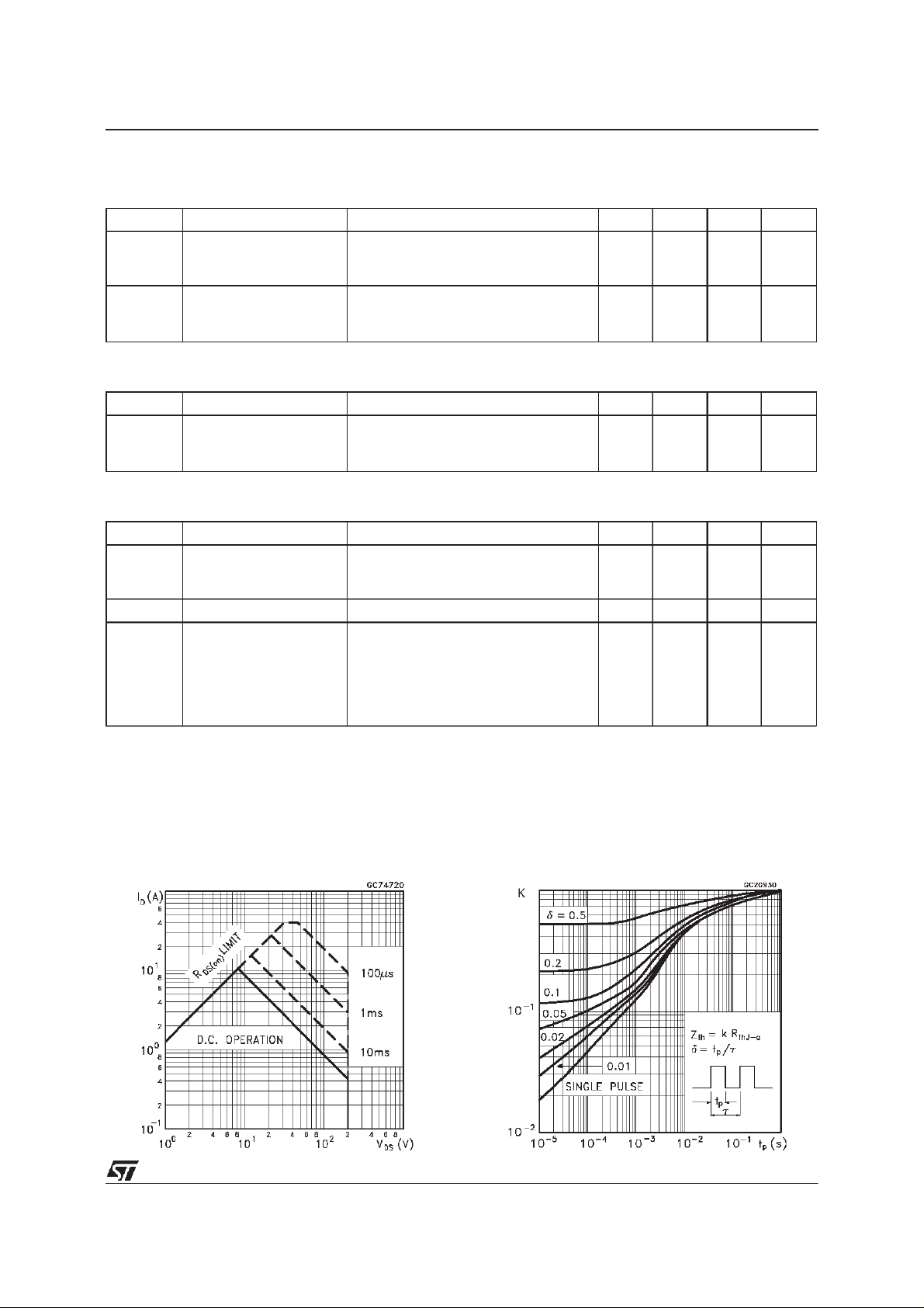
SafeOperating Area ThermalImpedance
3/8
Page 4

STB10NB20
OutputCharacteristics
Transconductance
TransferCharacteristics
Static Drain-sourceOn Resistance
Gate Charge vs Gate-sourceVoltage
4/8
CapacitanceVariations
Page 5

STB10NB20
NormalizedGate ThresholdVoltage vs
Temperature
Source-drainDiode Forward Characteristics
NormalizedOn Resistancevs Temperature
5/8
Page 6

STB10NB20
Fig. 1: Unclamped Inductive Load Test Circuit
Fig. 3: Switching Times Test Circuits For
ResistiveLoad
Fig. 2: Unclamped InductiveWaveform
Fig. 4: Gate Chargetest Circuit
Fig. 5: Test Circuit For InductiveLoad Switching
And Diode Recovery Times
6/8
Page 7

TO-263 (D2PAK) MECHANICAL DATA
STB10NB20
DIM.
MIN. TYP. MAX. MIN. TYP. MAX.
A 4.3 4.6 0.169 0.181
A1 2.49 2.69 0.098 0.106
B 0.7 0.93 0.027 0.036
B2 1.25 1.4 0.049 0.055
C 0.45 0.6 0.017 0.023
C2 1.21 1.36 0.047 0.053
D 8.95 9.35 0.352 0.368
E 10 10.28 0.393 0.404
G 4.88 5.28 0.192 0.208
L 15 15.85 0.590 0.624
L2 1.27 1.4 0.050 0.055
L3 1.4 1.75 0.055 0.068
mm inch
E
A
C2
L2
D
L
L3
B2
B
A1
C
G
P011P6/C
7/8
Page 8

STB10NB20
Information furnished is believed to be accurate and reliable. However, STMicroelectronics assumes no responsibility forthe consequences
of use of such information nor for any infringement of patents or other rights of third parties which may result from its use. No license is
granted by implication or otherwise under any patent or patent rights of STMicroelectronics. Specification mentioned in this publication are
subject to change without notice. This publication supersedes and replaces all informationpreviously supplied. STMicroelectronics products
are not authorized for use as critical components in life support devices or systems without express written approval of STMicroelectronics.
The ST logo is a trademarkof STMicroelectronics
1998 STMicroelectronics – Printed in Italy – All Rights Reserved
STMicroelectronics GROUP OF COMPANIES
Australia - Brazil - Canada - China - France -Germany - Italy - Japan -Korea - Malaysia -Malta - Mexico - Morocco - The Netherlands -
Singapore - Spain - Sweden - Switzerland - Taiwan - Thailand - United Kingdom - U.S.A.
http://www.st.com
.
8/8
 Loading...