

Page 1
• LOW NOISE FIGURE: NFmin = 0.9dB
@ 1.8GHz, 5mA, 2V
• HIGH OUTPUT IP3 = 24dBm
@ 1.8GHz, 20mA, 2V
• GOOD RUGG ED NESS BVceo = 4.5 V
• TRANSITION FRE QU E NC Y 45 GHz
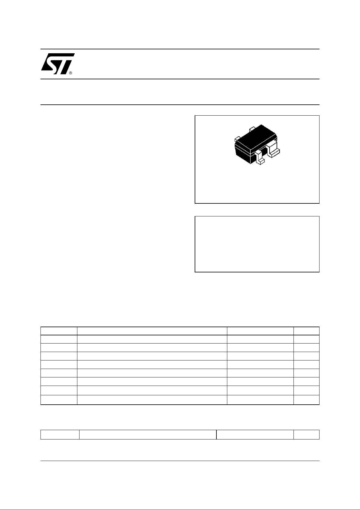
• ULTRA MINIATURE SOT343 PACKAGE
START540
NPN Silicon RF Transistor
SOT343 (SC70)
ORDER CODE
START540TR
BRANDING
540
DESCRIPTION
The START540 is a member of the START family
that provide the market with the state of the art of RF
silicon process. Manufacturated in the third
generation of ST proprietary bipolar process, it
APPLICATIONS
• LNA FOR GSM/DCS, DECT, PDC, PCS,
PCN, CDMA, W-CDMA
• GENERAL PURPOSE 500MHz-5GHz
offers the highest linearity with excellent Noise
Figure for 4.5V breakdown voltage(BVceo).
It reaches performance level only achieved with
GaAs products before.
ABSOLUTE MAXIMUM RATINGS
Symbol Parameter Value Unit
V
ceo
V
cbo
V
ebo
I
c
I
b
P
tot
T
stg
T
j
Collector emitter voltage 4.5 V
Collector base voltage 15 V
Emitter base voltage 1.5 V
Collector current 40 mA
Base current 4 mA
Total dissipation, Ts = 101
Storage temperature -65 to 150
Max. operating junction temperature 150
180 mW
o
C
o
C
ABSOLUTE MAXIMUM RATINGS
R
thjs
Thermal Resistance Junction soldering point 270
o
C/W
1/7July, 3 2002
Page 2
START540
w
ELECTRICAL CHARACTERISTICS (Tj=25 oC,unless otherwise specified)
Symbol Parameter Test Conditions Min. Typ. Max. Unit
I
cbo
I
ebo
Hfe DC current gain Ic = 20mA, Vce = 3V 100 160
NFmin Minimim noise figure
Ga NFmin associated gain Ic = 5mA, Vce = 2V, f = 1.8GHz 16 dB
|S21|
Gms
P
-1dB
OIP3
Note(1) : Gm s = | S21 / S12 |
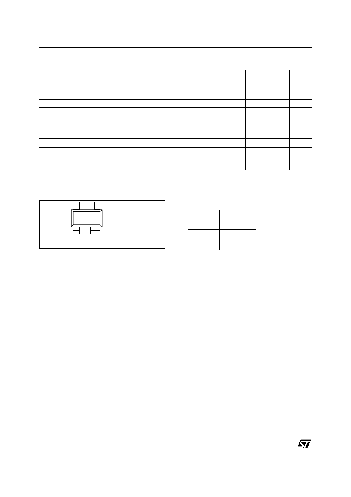
PINOUT
Collector cutoff current Vcb = 5V, Ie = 0A 150 nA
Emitter-base cutoff
current
2
(1)
Insertion power gain Ic = 20mA, Vce = 2V, f = 1.8GHz 19.5 dB
Maximum stable gain Ic = 20mA, Vce = 2V, f = 1.8GHz 22.7 dB
1dB compression point Ic = 20mA,Vce = 2V, f = 1.8GHz 13 dBm
Ouput third order
intercept point
4
3
Top vie
12
SOT343
Veb = 1.5V, Ic = 0A 15 µA
Ic = 5mA, Vce = 2V, f = 1.8GHz,
Ic = 20mA,Vce = 2V, f = 1.8GHz 24 dBm
Z
s
= Zsopt
0.9 dB
PIN CONNECTION
Pin No. Description
1BASE
3 COLLECTOR
2,4 EMITTER
2/7
Page 3

COMMON EMITTER S-PARAMETERS ( VCE = 2V, IC = 20mA )
START540
f
S
11
S
21
S
12
GHz MAG ANG MAG ANG MAG ANG MAG ANG
0.1 0.699 -21.6 42.32 164.0 0.009 8 8.9 0.942 -12.2
0.5 0.545 -89.7 27.82 119.9 0.027 5 8.1 0.642 -50.6
0.9 0.480 -130.0 18.42 98.1 0.0 36 48.1 0.431 -70.6
1 0.476 -137.4 16.86 94.0 0.0 38 47.2 0.397 -74.7
1.5 0.483 -166.9 11.63 76.9 0.0 48 41.6 0.272 -96.2
1.8 0.494 179.6 9.63 68. 2 0.052 38.8 0.220 -110.7
2 0.503 172.2 8.49 63. 1 0.055 36.7 0.193 -123.3
2.5 0.513 157.6 6.46 53. 6 0.061 31.7 0.148 -154.4
3 0.533 147.8 5.34 45. 9 0.069 26.7 0.142 -171.4
3.5 0.551 139.6 4.54 36. 6 0.077 21.2 0.153 177.9
4 0.559 133.8 3.87 28. 3 0.085 13.7 0.154 162.7
COMMON EMITTER S-PARAMETERS ( VCE = 2V, IC = 5mA )
f
S
11
GHz MAG A NG MAG ANG MAG ANG MAG ANG
0.5 0.816 -50.5 14.56 140.8 0.038 6 5.8 0.879 -30.3
S
21
S
12
S
22
S
22
0.9 0.715 -84.6 11.92 118.2 0.058 4 8.4 0.720 -49.0
1 0.695 -92.5 11.32 113.2 0.061 4 5.0 0.685 -53.1
1.5 0.620 -128.0 8.64 91. 5 0.075 30.9 0.515 -71.9
1.8 0.589 -145.6 7.39 80. 9 0.080 23.8 0.425 -81.8
2 0.581 -156.1 6.66 74. 5 0.080 19.3 0.374 -88.4
2.5 0.570 -167.6 5.87 8.0 0.082 14.8 0.316 -96.8
3 0.572 167.6 4.37 51. 7 0.085 5.7 0.225 -166.8
3.5 0.585 155.3 3.74 40. 4 0.090 1.1 0.208 -128.4
4 0.592 146.1 3.20 30. 6 0.094 -5.0 0.184 -141.2
COMMON EMITTER NOISE-PARAMETERS ( VCE = 2V, IC = 5mA )
f
F
min
Γ
opt
R
n
r
n
GHz dB MAG ANG Ω -dBdB
1.8 0.91 0.39 100.8 6.4 0.128 17.38 1.12
2 0.96 0.48 115.2 6.38 0.127 16.47 1.22
2.5 1.01 0.48 136.8 5.94 0 .118 14.35 1.34
3 1.14 0.46 163 5.6 0 .112 12.82 1.38
3.5 1.3 0.39 -160 5.2 0.104 11.46 1.42
4 1.4 0.32 -122.4 5 0.1 10.12 1.66
|S21|
2
F
50
3/7
Page 4

START540
SPICE PARAMETERS (Gummel-Poon Model, Berkley-SPICE 2G.6 Syntax)
TRANSISTOR CHIP DAT A
Symbol Value Symbol Value Symbol Value
TMEAS 27.0 FC 0.66 XJBC 0.53
IS 1.00E-16 EG 1.12 XTI 3.76
ISE 1.58E-1 1 NF 1 BF 320
NR 1 NE 3.27 VAF 70
ISC 1.55E-15 BR 9.52 VAR 2.3
o
IKF
TR 7E-10 PTF 32.0 VTF 27.9
XTF 9.84 ITF 0.498 MJE 0.497
RB 10.8 RBM 2.94 MJC 0.292
RC 3.77 RE 0.42 MJS 0.245
CJE 421E-15 VJE 1.03 IKR 8.32E-3
CJC 160E-15 VJC 0.6 XTB -0.54
CJS 112E-15 VJS 0.4
{0.217*((T(
300.15)^(-1.63)}
C)+273.15)/
NC 1.495 TF 3.0E-12
PACKAGE EQUIVALENT CIRCUIT
B . .
L4
L=0. 6 nH
L3 L5 L6
L=0.35 nH
C1
C2
C=66 fF
B’ C’
Transistor
Chip
E’
L=0. 1 nH
L1
.
L=0.05 nHL2
.
E
C3
C=334 fF C=436 fF
L=0.3 nH L=0.6 nH
. .
C
In order to avoid high complexity of the package equivalent circuit, the two emitter leads of SOT-343
package are combined in one electrical connection.
FOR MORE ACCURACY SIMULATION IN SATURATION REGION :
Adding the 5 Spice parameters showed in Table A and using ST Spice Library (available on request) you
can achieve a more ac curacy simulation in the saturation regi on. ST Spice library i s compatible with
following simulators: ELDO MENTOR (an y version), SPECT RE CADENCE (any version), ADS (version
2001 only).
Table A Table A (Spice Parameters extracted in saturation region)
RW Vjj ENP VRP RP
1.173 0.8 2.085 {4.12*((TEMPER+273.15)/300.15)^(0.303)} 1.00E-6
4/7
Page 5

START540
TAPE & REEL DIMENSIONS
mm
MIN. TYP. MAX
A 178.5 179 179.5
C 12.8 13.0 13.5
D 20.2
N 54.5 55 55.5
T 14.4
Ao 2.25
Bo 2.7
Ko 1.2
Po 3.8 (cumulative 10 Po) 4.0 4.2 (cumulative 10 Po)
P 4.0
DEVICE ORIENTATION
TOP VIEW END VIEW
540 540 540 540
5/7
Page 6

START540
PACKAGE DIMENSIONS SOT343 (SC-70 4 leads)
1.30
1.15-1.35
2.00-2.20
1.90-2.10
0.80-1.00
0.25-0.35 0.00-0.10
1.15
0.55-0.65
1.15-1.35
0.45
0.10-0.20
6/7
Page 7

START540
p
Information furnished is believed to be ac curate and reliable. Howev er, STMicroelec tronics assumes no responsibility for the consequen ces
of use of such information nor for any infringement of patents or other rights of third parties which may result from its use. No license is granted
by implic ation or otherwise u nder any pat ent or patent rights of STMicroelectron i cs . Specifications mentioned in this public at i on are subject
to change without notice. This publication supersedes and replaces all information previously supplied. STMicroelectronics product s are not
authorized for use as cri t i cal compone nts in life support devices or systems without express written approval of STMi croelect roni cs .
The ST log o i s registered trademark of STM i croelectronics
2002 STMicroelectroni cs - All Rights Reserved
All other names are the property of their resp ective owner s.
Australi a - Brazil - Canada - China - Finland - France - Germa ny - Hong Kong - India - Israel - Italy - Japan -
Malaysia - Malta - Morocco - Singapore - Spain - Sweden - Switzerland - United Kingdom - U.S.A.
STMicroelectron ics GROUP OF COMPANIES
htt
://www.st.com
7/7
 Loading...