

Page 1
• LOW NOISE FIGURE: NFmin = 1.1dB
@ 1.8GHz, 2mA, 2V
• COMPRESSION P1dB = 5dBm
@ 1.8GHz, 5mA, 2V
• TRANS I TI ON FR E QU E NC Y 42 GHz
• LOW CURRENT CONSUMPTION
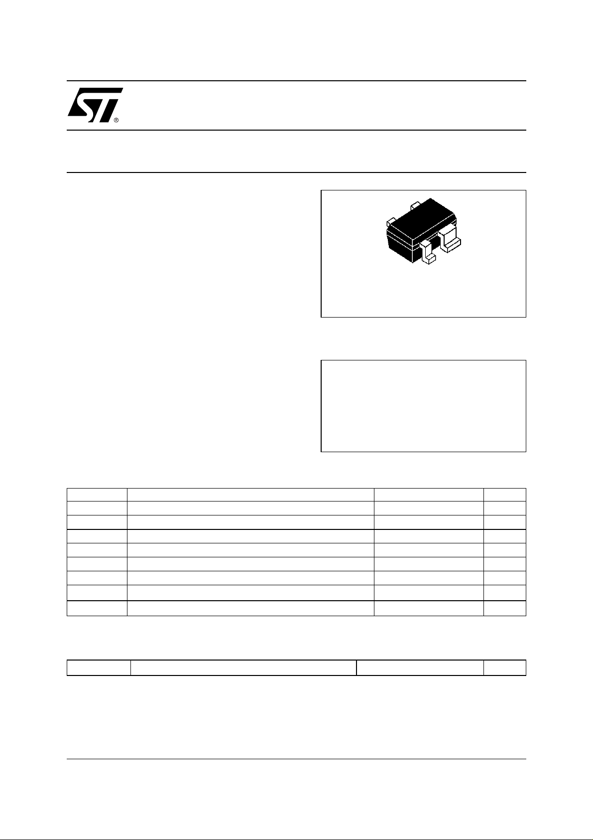
• ULTRA MINIATURE SOT343 PACKAGE
START405
NPN Silicon RF Transistor
SOT343 (SC70)
ORDER CODE
START405TR
BRANDING
405
DESCRIPTION
The START405 is a member of the START family
that provide the state of the art of RF silicon process
APPLICATIONS
to the market. Manufacturated in the third
generation of ST proprietary bipolar process, it
offers the best mix of gain and NF for given
breakdown voltage(BVceo).
• LNA FOR GSM/DCS, DECT, PCS, PCN,
CDMA, W-CDMA
• GENERAL PURPOSE 500MHz-5GHz
It offers performance level only archi ve d with G aAs
products before.
ABSOLUTE MAXIMUM RATINGS
Symbol Parameter Value Unit
V
ceo
V
cbo
V
ebo
I
c
I
b
P
tot
T
stg
T
j
Collector emitter voltage 4.5 V
Collector base voltage 15 V
Emitter base voltage 1.5 V
Collector current 10 mA
Base current 1 mA
Total dissipation, Ts = TBD
Storage temperature -65 to 150
Max. operating junction temperature 150
45 mW
o
C
o
C
ABSOLUTE MAXIMUM RATINGS
R
thjs
Thermal Resistance Junction soldering point 270
o
C/W
1/7July, 3 2002
Page 2

START405
w
ELECTRICAL CHARACTERISTICS (Tj=25 oC,unless otherwise specified)
Symbol Parameter Test Conditions Min. Typ. Max. Unit
I
cbo
I
ebo
Hfe DC current gain Ic = 5mA, Vce = 4V 160
NFmin Minimim noise figure Ic = 2mA, Vce = 2V, f = 1.8GHz 1.1 dB
Ga NFmin associated gain Ic = 2mA, Vce = 2V, f = 1.8GHz 19 dB
|S21|
Gms
P
-1dB
OIP3
Note(1): Gms = | S21 / S12 |
PINOUT
Collector cutoff current Vcb =5V, Ie = 0A 150 nA
Emitter-base cutoff
current
2
(1)
Insertion power gain Ic = 5mA, Vce = 2V, f = 1.8GHz 17.4 dB
Maximum stable gain Ic = 5mA, Vce = 2V, f = 1.8GHz 24.2 dB
1dB compression point Ic = 5mA,Vce = 2V, f = 1.8GHz 5 dBm
Ouput third order
intercept point
4
3
Top vie
12
SOT343
Veb = 1.5V, Ic = 0A 15 µA
Ic = 5mA,Vce = 2V, f = 1.8GHz 15 dBm
PIN CONNECTION
Pin No. Description
1BASE
3 COLLECTOR
2,4 EMITTER
2/7
Page 3

SPICE PARAMETERS (Gummel-Poon Model, Berkley-SPICE 2G.6 Syntax)
TRANSISTOR CHIP DATA
Symbol Value Symbol Value Symbol Value
TMEAS 27.0 FC 0.5 XJBC 0.3
IS 1.9E-17 EG 1.12 XTI 3.57
ISE 1.58E-13 NF 1 BF 340
NR 1 NE 2.711 VAF 79
ISC 7.40E-17 BR 8.59 VAR 2.35
o
IKF
TR 7E-10 PTF 38 VTF 14.7
XTF 42 ITF 0.42 MJE 0.414
RB 34.07 RBM 6.1 MJC 0.266
RC 7.9 RE 1.25 MJS 0.22
CJE 111E-15 VJE 1.1 IKR 2.29E-3
CJC 53E-15 VJC 0.69 XTB -0.744
CJS 33E-15 VJS 0.4
PACKAGE EQUIVALENT CIRCUIT
{0.151*((T(
300.15)^(-1.774)}
C)+273.15)/
NC 1.312 TF 4.1E-12
C2
C2
C=5 fF
C=5 fF
START405
L4
.
.
B .
B .
In order to avoid high complexity of the package equivalent circuit, the two emitter leads of SOT-343
package are combined in one electrical connection.
FOR MORE ACCURACY SIMULATION IN SATURATION REGION :
Adding the 5 Spice parameters showed in Table A and using ST Spice Library (available on request) you
can achieve a more accu racy simulation in the saturation region. ST Spice library is compa tible with
following simulators: ELDO MENTOR (any version), SPECTRE CADENCE (any version), ADS (version
2001 only).
Table A (Spice Parameters extracted in saturation region)
RW Vjj ENP VRP RP
L4
L=0.6 nH
L=0.6 nH
B’ C’
B’ C’
L3 L5 L6
L3 L5 L6
L=0.35 nH
L=0.35 nH
C1
C1
Transistor
Transistor
Chip
Chip
E’
E’
L=0.3 nH
L=0.3 nH
L1
L1
.
.
L=0.15 nHL2
L=0.15 nHL2
.
.
E
E
..
L=0.3 nH L=0.6 nH
L=0.3 nH L=0.6 nH
C3
C3
C=30 0 fFC=430 fF
C=30 0 fFC=430 fF
..
C
C
2.594 0.769 2.045 {8.67*((TEMPER+273.15)/300.15)^(0.839)} 1.00E-6
3/7
Page 4

START405
COMMON EMITTER S-PARAMETERS ( VCE = 2V, IC = 5mA )
S
FREQ
(MHz)
0.1
0.5
0.9
1
1.5
1.8
2
2.5
3
3.5
4
IS11IIS
∠Φ
21
0.903 -5 12.29 176 0.007 95 0.991 -2
0.882 -23 10.96 174 0.014 97 0.971 -11
0.825 -38 9.71 174 0.021 98 0.918 -19
0.809 -41 9.42 175 0.022 99 0.906 -20
0.713 -53 8.11 177 0.027 107 0.850 - 24
0.674 -58 7.43 180 0.028 114 0.829 - 27
0.642 -61 6.99 178 0.028 122 0.820 - 28
0.579 -64 6.01 172 0.028 148 0.815 - 30
0.523 -64 5.12 164 0.030 175 0.815 - 31
0.462 -67 4.31 156 0.039 131 0.787 - 35
0.372 -78 3.48 146 0.065 94 0.644 -41
S
IIS
∠Φ
IS12∠Φ IS22IS22∠Φ
12
4/7
Page 5

START405
TAPE & REEL DIMENSIONS
mm
MIN. TYP. MAX
A 178.5 179 179.5
C 12.8 13.0 13.5
D 20.2
N 54.5 55 55.5
T 14.4
Ao 2.25
Bo 2.7
Ko 1.2
Po 3.8 (cumulative 10 Po) 4.0 4.2 (cumulative 10 Po)
P 4.0
DEVICE ORIENTATION
TOP VIEW END VIEW
405 405 405 405
5/7
Page 6

START405
PACKAGE DIMENSIONS SOT 343 (SC-70 4 leads)
1.30
1.15-1.35
2.00-2. 20
1.90-2. 10
0.80-1. 00
0.25-0 .35 0.00- 0.10
1.15
0.55-0.65
1.15-1.35
0.45
0.10-0.20
6/7
Page 7

START405
p
Information furnished is believed to be ac curate and reliable. Howev er, STMicroelec tronics assumes no responsibility for the consequen ces
of use of such information nor for any infringement of patents or other rights of third parties which may result from its use. No license is granted
by implic ation or otherwise u nder any pat ent or patent rights of STMicroelectron i cs . Specifications mentioned in this public at i on are subject
to change without notice. This publication supersedes and replaces all information previously supplied. STMicroelectronics product s are not
authorized for use as cri t i cal compone nts in life support devices or systems without express written approval of STMi croelect roni cs .
The ST log o i s registered trademark of STM i croelectronics
2002 STMicroelectroni cs - All Rights Reserved
All other names are the property of their resp ective owner s.
Australi a - Brazil - Canada - China - Finland - France - Germa ny - Hong Kong - India - Israel - Italy - Japan -
Malaysia - Malta - Morocco - Singapore - Spain - Sweden - Switzerland - United Kingdom - U.S.A.
STMicroelectron ics GROUP OF COMPANIES
htt
://www.st.com
7/7
 Loading...